RF POWER MODULE
MOBILE APPLICATIONS
.
MOBILE CLASS C POWER AMPLIFIER
.
806 - 870 MHz
.
12.5 VOLTS
.
INPUT/OUTPUT 50 OHMS
.
P
O UT
=
20 W MIN.
.
GAIN
=
19 dB MIN.
DESCRIPTION
The TSTM872-20 module is designed for high
power, high efficiency, analog private mobile
radio systems in the 806 - 870 MHz frequency
range.
A significant advantage of this module is its
high RF power output performance and very
low standby current.
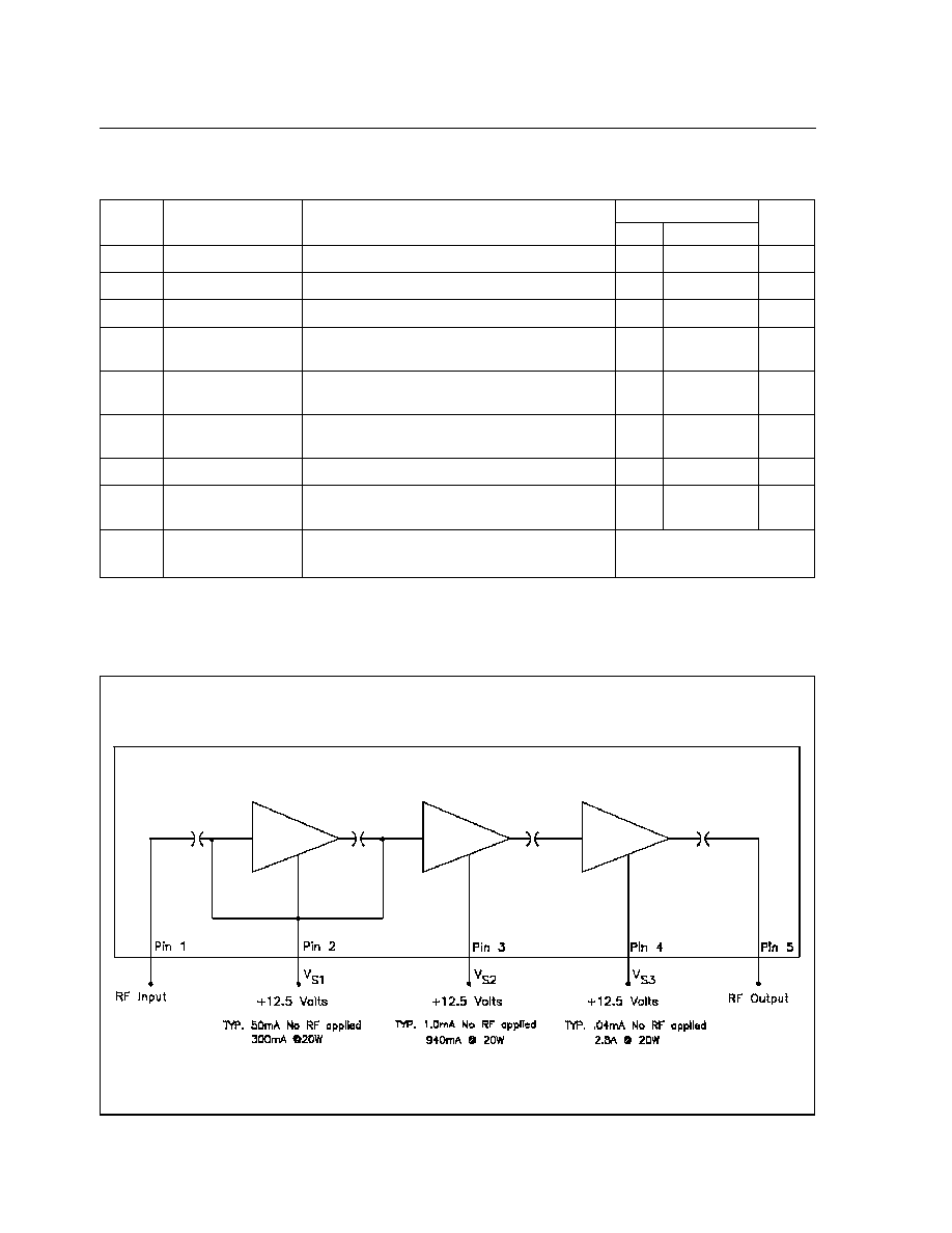
PIN CONNECTION
ABSOLUTE MAXIMUM RATINGS (Tcase
=
25
∞
C)
Symbol
Parameter
Value
Uni t
V
S1
, V
S 2
, V
S 3
DC Supply Voltage
16
Vdc
P
IN
RF Input Power
400
mW
P
OUT
RF Output Power
25
W
T
S TG
Storage Temperature
-
30 to +100
∞
C
T
C
Operating Case Temperature
-
30 to +100
∞
C
TSTM872-20
1. RF Input
2. 12.5 Vdc V
S1
3. 12.5 Vdc V
S2
4. 12.5 Vdc V
S3
5. RF Output
ORDER CODE
TSTM872-20
BRANDING
TSTM872-20
PRODUCT DEVELOPMENT DATA SHEET
This data sheet contains the design criteria and target specifications for a product which is currently under
development by SGS-THOMSON. The design criteria and specifications of this item could change prior
to introduction and SGS-THOMSON assumes no liability for use of information contained herein.

APPLICATIONS RECOMMENDATIONS
OPERATION LIMITS
The TSTM872-20 power module should never be
operated under any condition which exceeds the
Absolute Maximum Ratings presented on this
data sheet. Nor should the module be operated
continuously at any of the specified maximum rat-
ings. If the module is to be subjected to one or
more of the maximum rating conditions, care
must be taken to monitor other parameters which
may be affected.
DECOUPLING
Failure to properly decouple any of the voltage
supply pins will result in oscillations at certain op-
erating frequencies. Therefore, it is recommended
that these pins be bypassed as indicated in the
Module DC and Test Fixture Configuration draw-
ing of this data sheet.
MODULE MOUNTING
To insure adequate thermal transfer from the
module to the heatsink, it is recommended that a
satisfactory thermal compound such as Dow
Corning 340, Wakefield 120-2 or equivalent be
applied between the module flange and the
heatsink.
The heatsink mounting surface under the module
should be flat to within +/- 0.05 mm (+/- 0.002
inch). The module should be mounted to the
heatsink using 3.5 mm (or 6-32) or equivalent
screws torques to 5-6 kg-cm (4-6 in-lb).
The module leads should be attached to equip-
ment PC board using 180
∞
C solder applied to the
leads with a properly grounded soldering iron tip,
not to exceed 195
∞
C, applied a minimum of 2 mm
(0.080") from the body of the module for a dura-
tion not to exceed 15 seconds per lead. It is im-
perative that no other portion of the module, other
than the leads, be subjected to temperatures in
excess of 100
∞
C (maximum storage temperature),
for any period of time, as the plastic moulded
cover, internal components and sealing adhesives
may be adversely affected by such conditions.
Due to the construction techniques and materials
used within the module, reflow soldering of the
flange heatsink or leads, is not recommended.
TSTM872-20
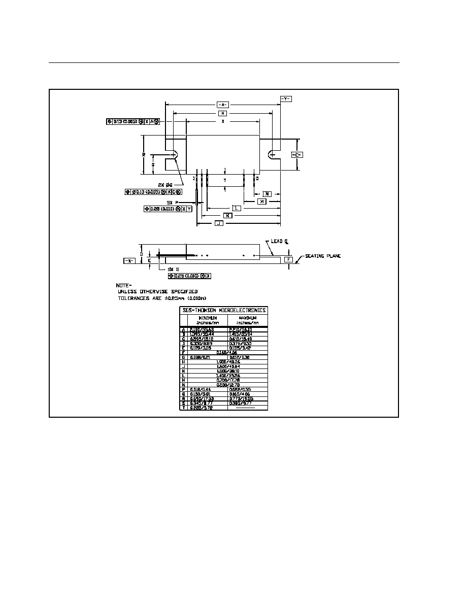
PACKAGE MECHANICAL DATA
Ref.: Dwg. No. M12-030 rev. C
Informatio n furnished is bel ieved to be accurate and reli abl e. However, SGS-THOMSON Microelectr onics assumes no respon-
sibili ty for the consequences of use of such information nor for any infringement of patents or other rig hts of third parties which
may result fr om its use. No license is granted by implication or otherwise under any patent or patent rights of S GS-T HOMSON
Microelectronics. Specifications mentioned in this publication are subject to change wi thout notice. This publi cati on super sedes
and replaces all informatio n previously supplied. SGS-T HOMSON Microel ectronics products are not authorized for use as criti cal
components in life support devices or systems without express written approval of SGS-THOMSON Mi croele ctr oni cs.
©
1995 SG S-TH OMSON Mi croelectronics - A ll Ri ghts Reserved
SGS -T HOMSON Microelectronics GROUP OF COMPANIES
Australia - Br azil - Fr ance - Germany - Hong Kong - Italy - Japan - Korea - Malaysia - Malta - Morocco - The Netherlands -
Singapore - Spai n - Sweden - Switzerla nd - Tai wan - Thai la nd - United Kingdom - U.S .A.
TSTM872-20