 | –≠–ª–µ–∫—Ç—Ä–æ–Ω–Ω—ã–π –∫–æ–º–ø–æ–Ω–µ–Ω—Ç: VN800PT-E | –°–∫–∞—á–∞—Ç—å:  PDF PDF  ZIP ZIP |

1/24
October 2004
VN800S-E
VN800PT-E
HIGH SIDE DRIVER
Rev. 1
Table 1. General Features
s
CMOS COMPATIBLE INPUT
s
THERMAL SHUTDOWN
s
CURRENT LIMITATION
s
SHORTED LOAD PROTECTION
s
UNDERVOLTAGE AND OVERVOLTAGE
SHUTDOWN
s
PROTECTION AGAINST LOSS OF GROUND
s
VERY LOW STAND-BY CURRENT
s
REVERSE BATTERY PROTECTION (*)
s
IN COMPLIANCE WITH THE 2002/95/EC
EUROPEAN DIRECTIVE
DESCRIPTION
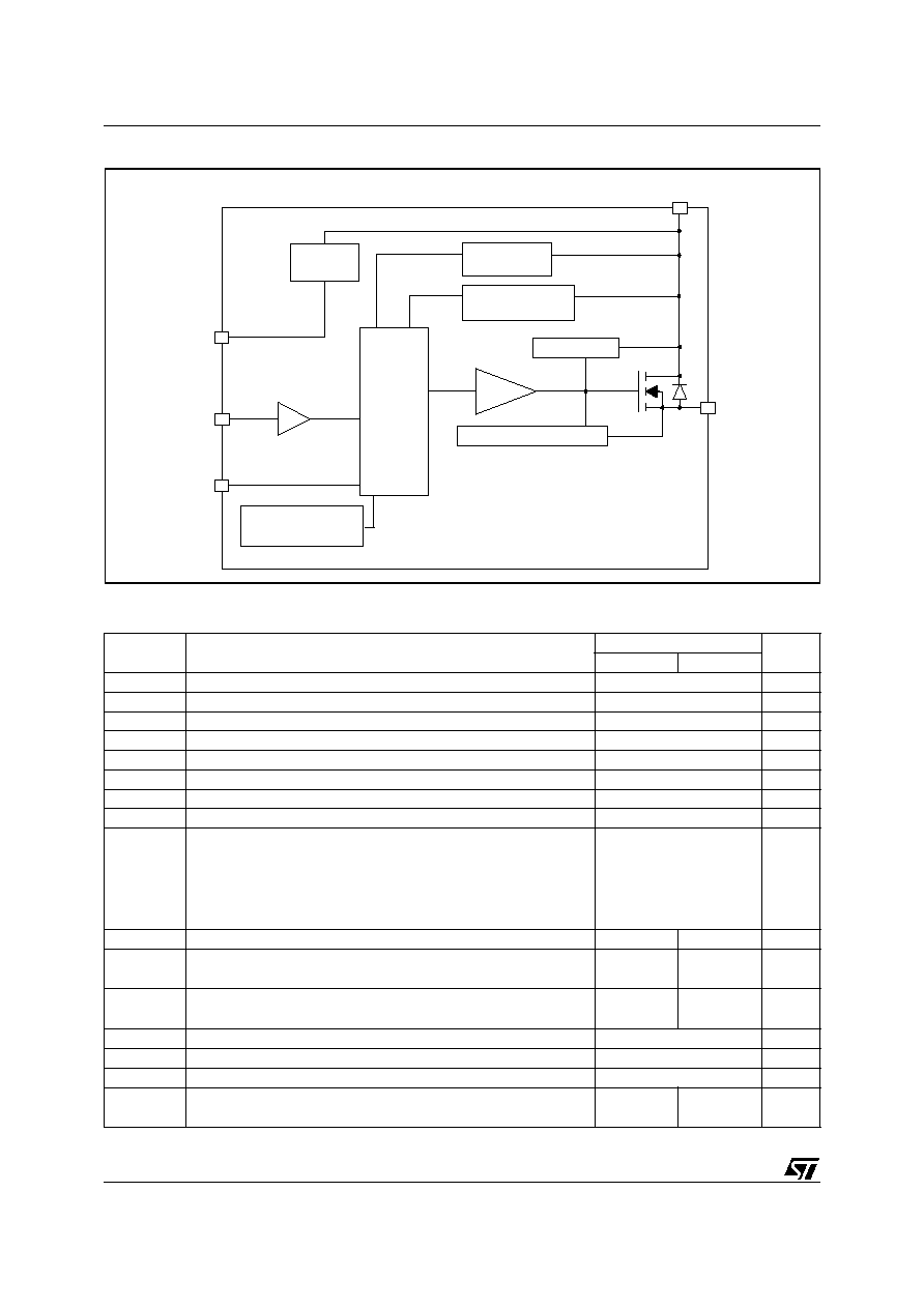
The VN800S-E, VN800PT-E are monolithic
devices made by using STMicroelectronics
VIPower M0-3 Technology, intended for driving
any kind of load with one side connected to
ground.
Active V
CC
pin voltage clamp protects the device
against low energy spikes.
Figure 1. Package
Active current limitation combined with thermal
shutdown and automatic restart protect the device
against overload. Device automatically turns off in
case of ground pin disconnection. This device is
especially suitable for industrial applications in
norms conformity with IEC1131 (Programmable
Controllers International Standard).
Table 2. Order Codes
Note: (*) See application schematic at page 10.
Type
R
DS(on)
I
OUT
V
CC
VN800S-E
VN800PT-E
135 m
0.7 A
36 V
SO-8
PPAK
Package
Tube
Tape and Reel
SO-8
VN800S-E
VN800STR-E
PPAK
VN800PT-E
VN800PTTR-E
VN800S-E / VN800PT-E
2/24
Figure 2. Block Diagram
Table 3. Absolute Maximum Ratings
Symbol
Parameter
Value
Unit
SO-8
PPAK
V
CC
DC Supply Voltage
41
V
- V
CC
Reverse DC Supply Voltage
- 0.3
V
- I
GND
DC Reverse Ground Pin Current
- 200
mA
I
OUT
DC Output Current
Internally Limited
A
- I
OUT
Reverse DC Output Current
- 6
A
I
IN
DC Input Current
+/- 10
mA
V
IN
Input Voltage Range
-3/+V
CC
V
V
STAT
DC Status Voltage
+ V
CC
V
V
ESD
Electrostatic Discharge (Human Body Model: R=1.5K
; C=100pF)
- INPUT
- STATUS
- OUTPUT
- V
CC
4000
4000
5000
5000
V
V
V
V
P
tot
Power Dissipation T
C
=25∞C
4.2
41.7
W
E
MAX
Maximum Switching Energy
(L=77.5mH; R
L
=0
; V
bat
=13.5V; T
jstart
=150∫C; I
L
=1.5A)
121
mJ
E
MAX
Maximum Switching Energy
(L=125mH; R
L
=0
; V
bat
=13.5V; T
jstart
=150∫C; I
L
=1.5A)
195
mJ
T
j
Junction Operating Temperature
Internally Limited
∞C
T
c
Case Operating Temperature
- 40 to 150
∞C
T
stg
Storage Temperature
- 55 to 150
∞C
L
max
Max Inductive Load (V
CC
=30V; I
LOAD
=0.5A; T
amb
=100∞C;
Rth
case>ambient
25∞C/W)
2
H
UNDERVOLTAGE
OVERTEMPERATURE
GND
INPUT
OUTPUT
OVERVOLTAGE
CURRENT
LIMITER
LOGIC
DRIVER
Power
CLAMP
STATUS
V
CC
CLAMP
DETECTION
DETECTION
DETECTION
V
CC
3/24
VN800S-E / VN800PT-E
Figure 3. Configuration Diagram (Top View) & Suggested Connections for Unused and N.C. Pins
Figure 4. Current and Voltage Conventions
Table 4. Thermal Data
(
1
) When mounted on FR4 printed circuit board with 0.5 cm
2
of copper area (at least 35
µ
thick) connected to all V
CC
pins.
(
2
) When mounted on FR4 printed circuit board with 2 cm
2
of copper area (at least 35
µ
thick).
(
3
) When mounted on FR4 printed circuit board with 0.5 cm
2
of copper area (at least 35
µ
thick) connected to all V
CC
pins.
(
4
) When mounted on FR4 printed circuit board with 6 cm
2
of copper area (at least 35
µ
thick).
Symbol
Parameter
Value
Unit
SO-8
PPAK
R
thj-case
Thermal Resistance Junction-case
Max
-
3
∞C/W
R
thj-lead
Thermal Resistance Junction-lead
Max
30
-
∞C/W
R
thj-amb
Thermal Resistance Junction-ambient
Max
Max
93 (
1
)
78 (
3
)
∞C/W
82 (
2
)
45 (
4
)
∞C/W
Connection / Pin Status
N.C.
Output
Input
Floating
X
X
X
X
To Ground
X
Through 10K
resistor
V
CC
V
CC
OUTPUT
OUTPUT
N.C.
GND
STATUS
INPUT
1
4
5
8
5
4
3
2
1
STATUS
OUTPUT
GND
INPUT
V
CC
SO-8
PPAK
INPUT
I
S
I
IN
V
IN
V
CC
STATUS
I
STAT
V
STAT
GND
V
CC
I
OUT
V
OUT
I
GND
OUTPUT
V
F
VN800S-E / VN800PT-E
4/24
ELECTRICAL CHARACTERISTICS (8V<V
CC
<36V; -40
∞C
<T
j
<150
∞C
unless otherwise specified)
Table 5. Power
Table 6. Switching (V
CC
=24V)
Table 7. Input Pin
Symbol
Parameter
Test Conditions
Min.
Typ.
Max.
Unit
V
CC
Operating Supply Voltage
5.5
36
V
V
USD
Undervoltage Shut-down
3
4
5.5
V
V
OV
Overvoltage Shut-down
36
42
V
R
ON
On State Resistance
I
OUT
=0.5A; T
j
=25∞C
I
OUT
=0.5A
135
270
m
m
I
S
Supply Current
Off State; V
CC
=24V; T
case
=25∞C
On State; V
CC
=24V
On State; V
CC
=24V; T
case
=100∞C
10
1.5
20
3.5
2.6
µ
A
mA
mA
I
LGND
Output Current at turn-off
V
CC
=V
STAT
=V
IN
=V
GND
=24V;V
OUT
=0V
1
mA
I
L(off1)
Off State Output Current
V
IN
=V
OUT
=0V
0
50
µ
A
I
L(off2)
Off State Output Current
V
IN
=V
OUT
=0V; V
CC
=13V; T
j
=125∞C
5
µ
A
I
L(off3)
Off State Output Current
V
IN
=V
OUT
=0V; V
CC
=13V; T
j
=25∞C
3
µ
A
Symbol
Parameter
Test Conditions
Min.
Typ.
Max.
Unit
t
d(on)
Turn-on Delay Time
R
L
=48
from V
IN
rising edge to
V
OUT
=2.4V
10
µ
s
t
d(off)
Turn-off Delay Time
R
L
=48
from V
IN
falling edge to
V
OUT
=21.6V
40
µ
s
dV
OUT
/
dt
(on)
Turn-on Voltage Slope
R
L
=48
from V
OUT
=2.4V to
V
OUT
=19.2V
See
relative
diagram
V/
µ
s
dV
OUT
/
dt
(off)
Turn-off Voltage Slope
R
L
=48
from V
OUT
=21.6V to
V
OUT
=2.4V
See
relative
diagram
V/
µ
s
Symbol
Parameter
Test Conditions
Min.
Typ.
Max.
Unit
V
INL
Input Low Level
1.25
V
I
INL
Low Level Input Current
V
IN
=1.25V
1
µ
A
V
INH
Input High Level
3.25
V
I
INH
High Level Input Current
V
IN
=3.25V
10
µ
A
V
I(hyst)
Input Hysteresis Voltage
0.5
V
I
IN
Input Current
V
IN
=V
CC
=36V 200
µ
A

5/24
VN800S-E / VN800PT-E
ELECTRICAL CHARACTERISTICS (continued)
Table 8. V
CC
- Output Diode
Table 9. Status Pin
Table 10. Protections (see note 1)
Note: 1. To ensure long term reliability under heavy overload or short circuit conditions, protection and related diagnostic signals must be
used together with a proper software strategy. If the device is subjected to abnormal conditions, this software must limit the duration
and number of activation cycles.
Figure 5.
Symbol
Parameter
Test Conditions
Min.
Typ.
Max.
Unit
V
F
Forward on Voltage
-I
OUT
=0.6A; T
j
=150∞C
0.6
V
Symbol
Parameter
Test Conditions
Min
Typ
Max
Unit
V
STAT
Status Low Output Voltage I
STAT
=1.6 mA
0.5
V
I
LSTAT
Status Leakage Current
Normal Operation; V
STAT
=V
CC
=36 V
10
µ
A
C
STAT
Status Pin Input
Capacitance
Normal Operation; V
STAT
= 5V
30
pF
Symbol
Parameter
Test Conditions
Min
Typ
Max
Unit
T
TSD
Shut-down Temperature
150
175
200
∞C
T
R
Reset Temperature
135
∞C
T
hyst
Thermal Hysteresis
7
15
∞C
T
SDL
Status Delay in Overload
Condition
T
j
>T
jsh
20
µ
s
I
lim
DC Short Circuit Current
V
CC
=24V; R
LOAD
=10m
0.7
2
A
V
demag
Turn-off Output Clamp
Voltage
I
OUT
=0.5 A; L=6mH
V
CC
-47
V
CC
-52
V
CC
-57
V
OVERTEMP STATUS TIMING
T
j
>T
jsh
V
IN
V
STAT
t
SDL
t
SDL