 | –≠–ª–µ–∫—Ç—Ä–æ–Ω–Ω—ã–π –∫–æ–º–ø–æ–Ω–µ–Ω—Ç: VNH100N04 | –°–∫–∞—á–∞—Ç—å:  PDF PDF  ZIP ZIP |

VNH100N04
"OMNIFET":
FULLY AUTOPROTECTED POWER MOSFET
TARGET DATA
September 1994
BLOCK DIAGRAM
TYPE
V
clamp
R
DS(on)
I
lim
VNH100N04
42 V
0.012
100 A
s
LINEAR CURRENT LIMITATION
s
THERMAL SHUT DOWN
s
SHORT CIRCUIT PROTECTION
s
INTEGRATED CLAMP
s
LOW CURRENT DRAWN FROM INPUT PIN
s
DIAGNOSTIC FEEDBACK THROUGH INPUT
PIN
s
ESD PROTECTION
s
DIRECT ACCESS TO THE GATE OF THE
POWER MOSFET (ANALOG DRIVING)
s
COMPATIBLE WITH STANDARD POWER
MOSFET
s
STANDARD TO-218 PACKAGE
DESCRIPTION
The VNH100N04 is a monolithic device made
using SGS-THOMSON Vertical Intelligent Power
M0 Technology, intended for replacement of
standard power MOSFETS in DC to 50 KHz
applications. Buit-in thermal shut-down, linear
current limitation and overvoltage clamp protect
the chip in harsh enviroments.
Fault feedback can be detected by monitoring the
voltage at the input pin.
TO-218
1/7

ABSOLUTE MAXIMUM RATING
Symbol
Parameter
Val ue
Uni t
V
D S
Drain-source Voltage (V
in
= 0)
Internally Clamped
V
V
in
I nput Voltage
18
V
I
D
Drain Current
Internally Limited
A
I
R
Reverse DC Output Current
-50
A
V
esd
Electrost atic Discharge (C= 100 pF, R=1.5 K
)
2000
V
P
tot
Total Dissipation at T
c
= 25
o
C
208
W
T
j
Operating Junction Temperature
Internally Limited
o
C
T
c
Case Operating Temperature
Internally Limited
o
C
T
stg
St orage Temperat ure
-55 to 150
o
C
THERMAL DATA
R
thj-cas e
R
thj- amb
Thermal Resist ance Junct ion-case
Max
Thermal Resist ance Junct ion-ambient
Max
0.6
30
o
C/ W
o
C/ W
ELECTRICAL CHARACTERISTICS (T
case
= 25
o
C unless otherwise specified)
OFF
Symbol
Parameter
Test Condi tions
Mi n.
Typ.
Max.
Unit
V
CLAM P
Drain-source Clamp
Voltage
I
D
= 30 A
V
in
= 0
36
42
48
V
V
CLTH
Drain-source Clamp
Threshold Voltage
I
D
= 2 mA
V
in
= 0
35
V
V
I NC L
I nput-Source Reverse
Clamp Voltage
I
in
= -1 mA
-1
-0.3
V
I
DS S
Zero Input Voltage
Drain Current (V
in
= 0)
V
DS
= 13 V
V
DS
= 25 V
50
200
µ
A
µ
A
I
ISS
Supply Current from
I nput Pin
V
DS
= 0 V
V
in
= 10 V
250
500
µ
A
ON (
)
Symbol
Parameter
Test Condi tions
Mi n.
Typ.
Max.
Unit
V
I S(th)
I nput Threshold
Voltage
V
DS
= V
in
I
D
= 1 mA
0.8
3
V
R
DS( on)
St atic Drain-source On
Resist ance
V
in
= 10 V
I
D
= 30 A
V
in
= 5 V
I
D
= 30 A
0.012
0.015
DYNAMIC
Symbol
Parameter
Test Condi tions
Mi n.
Typ.
Max.
Unit
g
fs
(
)
Forward
Transconductance
V
DS
= 13 V
I
D
= 30 A
40
S
C
oss
Output Capacit ance
V
DS
= 13 V
f = 1 MHz
V
in
= 0
1800
3000
pF
VNH100N04
2/7

ELECTRICAL CHARACTERISTICS (continued)
SWITCHING
Symbol
Parameter
Test Condi tions
Mi n.
Typ.
Max.
Unit
t
d(on)
t
r
t
d(off )
t
f
Turn-on Delay Time
Rise Time
Turn-off Delay Time
Fall Time
V
DD
= 15 V
I
d
= 30 A
V
gen
= 10 V
R
gen
= 10
(see figure 3)
100
400
900
400
TBD
TBD
TBD
TBD
ns
ns
ns
ns
t
d(on)
t
r
t
d(off )
t
f
Turn-on Delay Time
Rise Time
Turn-off Delay Time
Fall Time
V
DD
= 15 V
I
d
= 30 A
V
gen
= 10 V
R
gen
= 10
T
j
= 125
o
C
(see figure 3)
TBD
TBD
TBD
TBD
ns
ns
ns
ns
t
d(on)
t
r
t
d(off )
t
f
Turn-on Delay Time
Rise Time
Turn-off Delay Time
Fall Time
V
DD
= 15 V
I
d
= 30 A
V
gen
= 10 V
R
gen
= 1000
(see figure 3)
TBD
TBD
TBD
TBD
µ
s
µ
s
µ
s
µ
s
(di/dt)
on
Turn-on Current Slope
V
DD
= 15 V
I
D
= 30 A
V
in
= 10 V
TBD
A/
µ
s
Q
g
Total Gate Charge
V
DD
= 12 V
I
D
= 30 A
V
in
= 10 V
TBD
nC
SOURCE DRAIN DIODE
Symbol
Parameter
Test Condi tions
Mi n.
Typ.
Max.
Unit
V
S D
(
)
Forward On Volt age
I
SD
= 30 A
V
in
= 0
TBD
V
t
rr
Q
rr
I
RRM
Reverse Recovery
Time
Reverse Recovery
Charge
Reverse Recovery
Current
I
SD
= 30 A
di/dt = 100 A/
µ
s
V
DD
= V
T
j
= 150
o
C
(see test circuit, figure 5)
TBD
TBD
TBD
ns
µ
C
A
PROTECTION
Symbol
Parameter
Test Condi tions
Mi n.
Typ.
Max.
Unit
I
lim
Drain Current Limit
V
in
= 10 V
V
DS
= 13 V
70
100
140
A
t
dlim
St ep Response
Current Limit
V
in
= 10 V
V
D S
= 13V
TBD
µ
s
T
jsh
Overtemperature
Shutdown
150
170
190
o
C
T
jrs
Overtemperature Reset
135
o
C
I
gf
Fault Sink Current
V
in
= 10 V
V
DS
= 13 V
50
mA
E
as
Single Pulse
Avalanche Energy
st arting T
j
= 25
o
C
V
DD
= 20 V
V
in
= 10 V R
gen
= 1 K
L = mH
TBD
J
(
) Pulsed: Pul se dur ation = 300
µ
s, duty cycle 1.5 %
VNH100N04
3/7

During
normal
operation,
the
Input
pin
is
electrically connected to the gate of the internal
power MOSFET. The device then behaves like a
standard power MOSFET and can be used as a
switch from DC to 50 KHz. The only difference
from the user's standpoint is that a small DC
current (I
iss
) flows into the Input pin in order to
supply the internal circuitry.
The device integrates:
≠
OVERVOLTAGE
CLAMP
PROTECTION:
internally set at 42V, along with the rugged
avalanche
characteristics
of
the
Power
MOSFET stage give this device unrivalled
ruggedness and energy handling capability.
This feature is mainly important when driving
inductive loads.
≠
LINEAR CURRENT LIMITER CIRCUIT: limits
the drain current Id to Ilim whatever the Input
pin voltage. When the current limiter is active,
the device operates in the linear region, so
power dissipation may exceed the capability of
the
heatsink.
Both
case
and
junction
temperatures increase, and if this phase lasts
long enough, junction temperature may reach
the overtemperature threshold T
jsh
.
≠
OVERTEMPERATURE AND SHORT CIRCUIT
PROTECTION: these are based on sensing
the chip temperature and are not dependent on
the input voltage. The location of the sensing
element on the chip in the power stage area
ensures fast, accurate detection of the junction
temperature. Overtemperature cutout occurs in
the range 150 to 190
o
C, a typical value being
170
o
C. The device is automatically restarted
when the chip temperature falls below 135
o
C.
≠
STATUS FEEDBACK: In the case of an
overtemperature
fault
condition,
a
Status
Feedback is provided through the Input pin.
The internal protection circuit disconnects the
input from the gate and connects it instead to
ground via an equivalent resistance of 200
.
The failure can be detected by monitoring the
voltage at the Input pin, which will be close to
ground potential.
Additional features of this device are ESD
protection according to the Human Body model
and the ability to be driven from a TTL Logic
circuit (with a small increase in R
DS(on)
).
PROTECTION FEATURES
VNH100N04
4/7
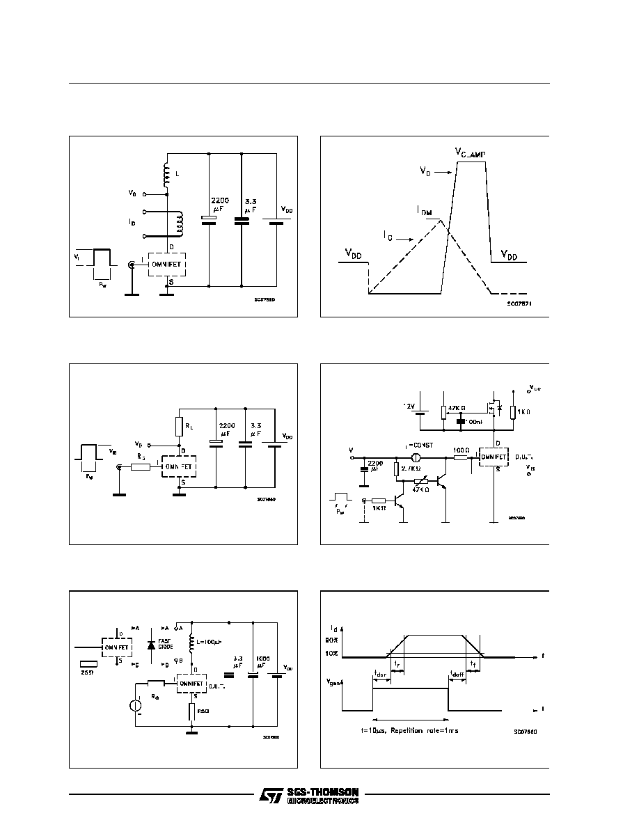
Fig. 2: Unclamped Inductive Waveforms
Fig. 3: Switching Times Test Circuits For
Resistive Load
Fig. 4: Input Charge Test Circuit
Fig. 1: Unclamped Inductive Load Test Circuits
Fig. 5: Test Circuit For Inductive Load Switching
And Diode Recovery Times
Fig. 6: Waveforms
VNH100N04
5/7