1
HV254
07/24/03
Supertex Inc. does not recommend the use of its products in life support applications and will not knowingly sell its products for use in such applications unless it receives an adequate "products liability
indemnification insurance agreement." Supertex does not assume responsibility for use of devices described and limits its liability to the replacement of devices determined to be defective due to
workmanship. No responsibility is assumed for possible omissions or inaccuracies. Circuitry and specifications are subject to change without notice. For the latest product specifications, refer to the
Supertex website: http://www.supertex.com. For complete liability information on all Supertex products, refer to the most current databook or to the Legal/Disclaimer page on the Supertex website.
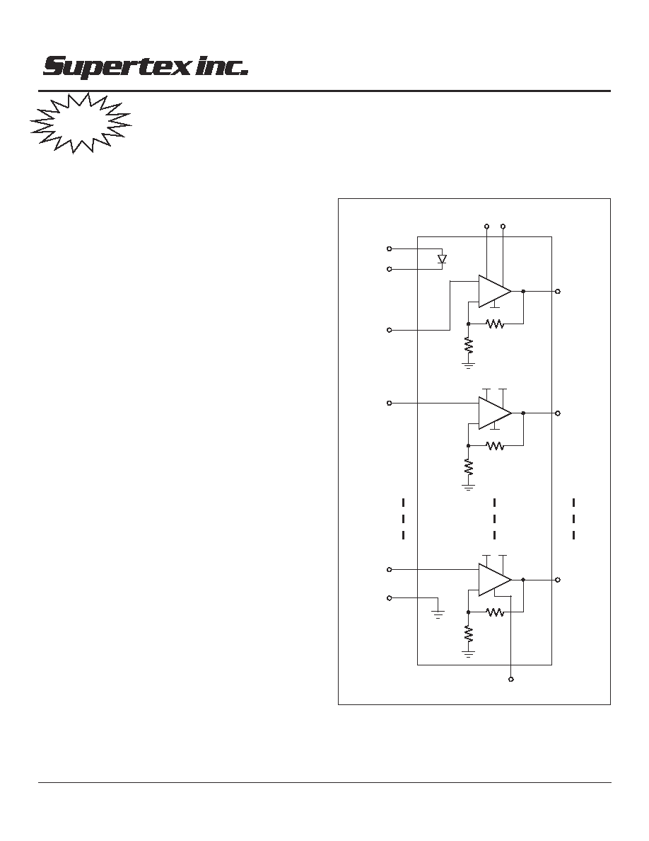
32-Channel High Voltage Amplifier Array
HV254
Features
32 independent high voltage amplifiers
Output voltage up to 250V
3V/
µ
s output slew rate
Fixed gain of 50V/V
High value internal feedback resistors
Very low operating current (typically 45
µ
A per channel)
Integrated silicon diode for temperature sensing
Application
MEMS (microelctromechanical systems) driver
Piezoelectric transducer driver
Optical crosspoint switches (using MEMS technology)
General Description
The Supertex HV254 is a 32-channel high voltage amplifier array
integrated circuit. It operates on a 275V high voltage supply and
two low voltage supplies: +5.0V and ≠5.0V. Each channel has its
own input and output. An integrated diode is included to help
monitor die temperature.
The input voltage can be from a dac with a voltage range of 0V
to the low voltage suply, V+. The output of the HV254FG will
swing from 7V to 250V. It cannot swing to ground. With the
internal gain set at 50V/V, a minimum input signal of 140mV will
still maintain linearity. Input voltages below 140mV can be
applied without damage to the device. The amplifier, however,
will be saturated. Typical output load is equivalent to a 125Mohm
resistor in parallel with a 100pF capacitor. The outputs have a
guaranteed slew rate of at least 3V/
µ
s. The internal closed loop
gain is set at a nominal value of 34.0dB (50V/V).
The HV254 is designed to operate with minimal power consump-
tion while maintaining a guaranteed slew rate of 3V/
µ
s. High
value resistors are used for the gain setting to minimize current
on the feedback path.
Block Diagram
HV
OUT
0
HV
OUT
1
V
PP
49R
R
V-
V+
PGND
V+
49R
R
V-
HV
OUT
31
V
PP
49R
R
V-
V+
V
IN
1
V
IN
0
V
IN
31
V
PP
Anode
Cathode
-
+
-
+
-
+
Demo Kit
Available
2
HV254
Absolute Maximum Ratings*
V
PP
, High voltage supply
275V
V+, Low voltage positive supply
7.0V
V-, Low voltage negative supply
-7.0V
HV
OUT
, Output voltage
0V to 275V
V
IN
, Analog input signal
0V to 5.0V
Storage temperature range
-65
∞
C to 150
∞
C
Maximum junction temperature
150
∞
C
* All voltages are referenced to device ground.
e
c
i
v
e
D
e
g
a
t
l
o
V
t
u
p
t
u
O
m
u
m
i
x
a
M
s
n
o
i
t
p
O
e
g
a
k
c
a
P
P
F
Q
M
d
a
e
L
0
0
1
e
i
D
4
5
2
V
H
V
0
5
2
G
F
4
5
2
V
H
X
4
5
2
V
H
Ordering Information
Electrical Characteristics
(Over operating conditions unless otherwise noted.)
l
o
b
m
y
S
r
e
t
e
m
a
r
a
P
n
i
M
p
y
T
x
a
M
s
t
i
n
U
s
n
o
i
t
i
d
n
o
C
s
n
o
t
i
d
n
o
C
g
n
i
t
a
r
e
p
O
V
P
P
y
l
p
p
u
s
e
v
i
t
i
s
o
p
e
g
a
t
l
o
v
h
g
i
H
0
5
5
7
2
V
+
V
y
l
p
p
u
s
e
v
i
t
i
s
o
p
e
g
a
t
l
o
v
w
o
L
5
7
.
4
0
.
5
5
2
.
5
V
-
V
y
l
p
p
u
s
e
v
i
t
a
g
e
n
e
g
a
t
l
o
v
w
o
L
5
7
.
4
-
0
.
5
-
5
2
.
5
-
V
I
P
P
V
P
P
t
n
e
r
r
u
c
y
l
p
p
u
s
0
.
1
5
.
2
A
m
V
P
P
.
V
m
0
4
1
t
a
t
e
s
s
t
u
p
n
i
ll
A
,
V
5
7
2
=
5
4
y
ll
a
c
i
p
y
T
µ
l
e
n
n
a
h
c
r
e
p
A
+
I
t
n
e
r
r
u
c
y
l
p
p
u
s
+
V
0
.
1
A
m
V
5
2
.
5
=
+
V
-
I
V
N
N
t
n
e
r
r
u
c
y
l
p
p
u
s
0
.
3
-
A
m
V
5
2
.
5
-
=
-
V
T
A
e
g
n
a
r
e
r
u
t
a
r
e
p
m
e
t
t
n
e
i
b
m
A
0
1
-
0
7
C
∞
T
J
e
g
n
a
r
e
r
u
t
a
r
e
p
m
e
t
n
o
i
t
c
n
u
J
0
1
-
D
B
T
C
∞
t
u
p
t
u
O
r
e
i
f
i
l
p
m
A
e
g
a
t
l
o
V
h
g
i
H
V
H
T
U
O
V
H
T
U
O
g
n
i
w
s
e
g
a
t
l
o
v
0
.
7
0
5
2
V
V
P
P
M
5
2
1
=
d
a
o
L
,
V
5
7
2
=
F
p
0
0
1
/
/
V
N
I
e
g
n
a
R
e
g
a
t
l
o
V
t
u
p
n
I
4
1
.
0
+
V
V
V
H
S
O
V
H
T
U
O
t
e
s
f
f
o
C
D
5
.
1
±
2
5
.
1
±
V
V
P
P
t
e
s
f
f
o
t
u
p
n
i
V
m
0
3
.
V
5
7
2
=
R
S
V
H
T
U
O
e
t
a
r
w
e
l
s
0
.
3
/
V
µ
s
V
P
P
M
5
2
1
=
d
a
o
L
,
V
5
7
2
=
F
p
0
0
1
/
/
R
B
F
e
c
n
a
d
e
p
m
i
k
c
a
b
d
e
e
F
8
2
1
M
A
V
n
i
a
g
p
o
o
l
d
e
s
o
l
C
5
.
7
4
0
.
0
5
5
.
2
5
V
/
V
W
B
V
H
T
U
O
h
t
d
i
w
d
n
a
b
l
e
n
n
a
h
c
B
d
3
-
0
.
5
z
H
K
V
P
P
V
5
7
2
=
C
D
A
O
L
V
H
T
U
O
d
a
o
l
e
v
i
t
i
c
a
p
a
c
0
0
0
1
F
p
)
t
f
i
r
d
x
a
m
(
y
t
il
i
b
a
t
S
0
0
5
V
m
V
H
t
a
d
e
r
u
s
a
e
M
T
U
O

3
HV254
l
o
b
m
y
S
r
e
t
e
m
a
r
a
P
n
i
M
p
y
T
x
a
M
s
t
i
n
U
s
n
o
i
t
i
d
n
o
C
Diode
V
I
P
e
g
a
t
l
o
v
e
s
r
e
v
n
i
k
a
e
P
0
.
5
V
e
d
o
n
a
o
t
e
d
o
h
t
a
c
V
F
p
o
r
d
e
d
o
i
d
d
r
a
w
r
o
F
8
.
0
V
e
d
o
h
t
a
c
o
t
e
d
o
n
a
,
A
m
0
.
2
=
f
I
I
F
t
n
e
r
r
u
c
e
d
o
i
d
d
r
a
w
r
o
F
0
.
2
A
m
e
d
o
h
t
a
c
o
t
e
d
o
n
a
T
C
V
F
t
n
e
i
c
i
f
f
e
o
c
e
r
u
t
a
r
e
p
m
e
t
D
B
T
C
∞
/
V
m
e
d
o
h
t
a
c
o
t
e
d
o
n
a
n
o
i
t
p
i
r
c
s
e
D
n
i
P
V
P
P
.
y
l
p
p
u
s
e
v
i
t
i
s
o
p
e
g
a
t
l
o
v
h
g
i
H
+
V
.
y
l
p
p
u
s
e
v
i
t
i
s
o
p
e
g
a
t
l
o
v
w
o
l
g
o
l
a
n
A
-
V
.
y
l
p
p
u
s
e
v
i
t
a
g
e
n
e
g
a
t
l
o
v
w
o
l
g
o
l
a
n
A
D
N
G
P
.
d
n
u
o
r
g
e
c
i
v
e
D
e
d
o
n
A
e
i
d
r
o
t
i
n
o
m
o
t
d
e
s
u
e
b
n
a
c
t
a
h
t
e
d
o
i
d
n
o
c
il
i
s
e
g
a
t
l
o
v
w
o
l
a
f
o
e
d
i
s
e
d
o
n
A
.
e
r
u
t
a
r
e
p
m
e
t
e
d
o
h
t
a
C
e
i
d
r
o
t
i
n
o
m
o
t
d
e
s
u
e
b
n
a
c
t
a
h
t
e
d
o
i
d
n
o
c
il
i
s
e
g
a
t
l
o
v
w
o
l
a
f
o
e
d
i
s
e
d
o
h
t
a
C
.
e
r
u
t
a
r
e
p
m
e
t
V
N
I
V
o
t
0
N
I
1
3
.
s
t
u
p
n
i
r
e
i
f
il
p
m
A
V
H
T
U
O
V
H
o
t
0
T
U
O
1
3
.
s
t
u
p
t
u
o
r
e
i
f
il
p
m
A
Acceptable Power Up Sequences
1) V
PP
2) V-
3) V+
4) Inputs & Anode
1) V+
2) V-
3) V
PP
4) Inputs & Anode
Acceptable Power Down Sequences
1) Inputs & Anode
2) V
PP
3) V+
4) V-
1) Inputs & Anode
2) V+
3) V-
4) V
PP
Power Up/Down Sequence
The device can be damaged due to improper power up / down
sequence. To prevent damage, please follow the acceptable
power up /down sequences and add two external diodes as
shown in the diagram below. The first diode is a high voltage
diode across Vpp and V+ where the anode of the diode is
connected to V+ and the cathode of the diode is connected to
Vpp. Any low current high voltage diode such as a 1N4004 will
be adequate. The second diode is a schottky diode across V-
and PGND where the anode of the schottky diode is connected
to V- and the cathode is connected to PGND. Any low current
schottky diode such as a 1N5817 will be adequate.
V+
Vpp
1N4004
or similar
V-
PGND
1N5817
or similar