 | –≠–ª–µ–∫—Ç—Ä–æ–Ω–Ω—ã–π –∫–æ–º–ø–æ–Ω–µ–Ω—Ç: TFA9842BJ | –°–∫–∞—á–∞—Ç—å:  PDF PDF  ZIP ZIP |

1.
General description
The TFA9842BJ contains two identical audio power amplifiers. The TFA9842BJ can be
used as two Single-Ended (SE) channels with a fixed gain of 26 dB.
The TFA9842BJ comes in a 9-pin DIL-bent-SIL (DBS9P) power package. The TFA9842BJ
is pin compatible with the TFA9841J, TFA9842J, TFA9843J and the TFA9843BJ.
The TFA9842BJ contains a unique protection circuit that is solely based on multiple
temperature measurements inside the chip. This gives maximum output power for all
supply voltages and load conditions with no unnecessary audio holes. Almost any supply
voltage and load impedance combination can be made as long as thermal boundary
conditions (number of channels used, external heatsink and ambient temperature) allow
it.
2.
Features
s
1 W to 7.5 W operation possibility
s
Soft clipping
s
Standby and mute mode
s
No on or off switching plops
s
Low standby current
s
High supply voltage ripple rejection
s
Outputs short-circuit protected to ground, supply and across the load
s
Thermally protected
s
Pin compatible with the TFA9841J, TFA9842J, TFA9843J and the TFA9843BJ.
3.
Applications
s
Televisions
s
Monitors
s
PC speakers
s
Boom boxes
s
Mini and micro audio receivers.
TFA9842BJ
2-channel audio amplifier (SE: 1 W to 7.5 W)
Rev. 01 -- 1 March 2004
Preliminary data sheet

9397 750 12847
© Koninklijke Philips Electronics N.V. 2004. All rights reserved.
Preliminary data sheet
Rev. 01 -- 1 March 2004
2 of 17
Philips Semiconductors
TFA9842BJ
2-channel auto amplifier (2
◊
SE)
4.
Quick reference data
5.
Ordering information
Table 1:
Quick reference data
Symbol
Parameter
Conditions
Min
Typ
Max
Unit
V
CC
supply voltage
operating
9
17
26
V
no signal
-
-
28
V
I
q
quiescent supply current
V
CC
= 17 V;
R
L
=
-
60
100
mA
I
stb
standby supply current
-
-
10
µ
A
P
o
output power
THD = 10 %;
R
L
= 4
;
V
CC
= 17 V
7
7.5
-
W
THD
total harmonic distortion
P
o
= 1 W
-
0.1
0.5
%
G
v
voltage gain
25
26
27
dB
SVRR
supply voltage ripple
rejection
f
ripple
= 1 kHz
-
60
-
dB
Table 2:
Ordering information
Type number
Package
Name
Description
Version
TFA9842BJ
DBS9P
plastic DIL-bent-SIL power package; 9 leads (lead
length 12/11 mm); exposed die pad
SOT523 -1
9397 750 12847
© Koninklijke Philips Electronics N.V. 2004. All rights reserved.
Preliminary data sheet
Rev. 01 -- 1 March 2004
3 of 17
Philips Semiconductors
TFA9842BJ
2-channel auto amplifier (2
◊
SE)
6.
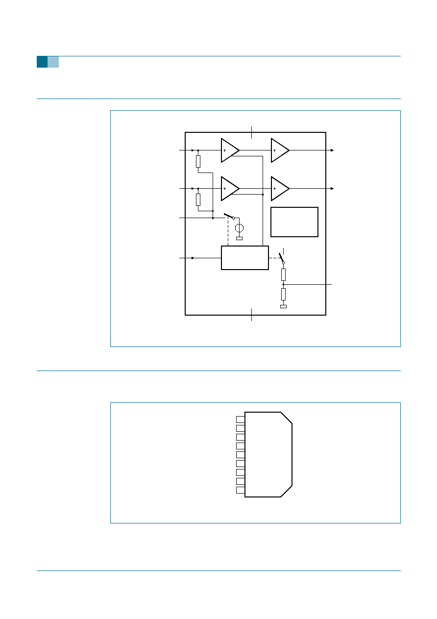
Block diagram
7.
Pinning information
7.1 Pinning
Fig 1.
Block diagram.
001aaa443
STANDBY
MUTE
ON
SHORT-CIRCUIT
AND
TEMPERATURE
PROTECTION
V
REF
0.5V
CC
V
CC
V
CC
9
4
IN1
IN2
OUT1
OUT2
SVR
CIV
MODE
1
3
7
8
2
6
5
GND
TFA9842BJ
60
k
60
k
Fig 2.
Pin configuration.
TFA9842BJ
001aaa444
2
1
3
4
5
6
7
8
9
V
CC
IN1
IN2
OUT1
OUT2
SVR
CIV
MODE
GND

9397 750 12847
© Koninklijke Philips Electronics N.V. 2004. All rights reserved.
Preliminary data sheet
Rev. 01 -- 1 March 2004
4 of 17
Philips Semiconductors
TFA9842BJ
2-channel auto amplifier (2
◊
SE)
7.2 Pin description
8.
Functional description
8.1 Input configuration
The input cut-off frequency is:
(1)
Application: R
i
= 60 k
and C
i
= 220 nF:
(2)
As shown in
Equation 2
large capacitor values for the inputs are not necessary; so the
switch-on delay during charging of the input capacitors can be minimized. This results in a
good low frequency response and good switch-on behavior.
8.2 Power amplifier
The power amplifier is a Single-Ended (SE) amplifier with an all-NPN output stage,
capable of delivering a peak output current of 3 A.
8.2.1 Output power measurement
The output power as a function of the supply voltage is measured on the output pins at
THD = 10 %; see
Figure 8
. The maximum output power is limited by the supply voltage of
26 V and the maximum available output current is 3 A (repetitive peak current). A
minimum load of 3
is required for V
CC
> 22 V; see
Figure 5
. The output power is
measured with one channel driven.
Table 3:
Pin description
Symbol
Pin
Description
IN2
1
input 2
OUT2
2
loudspeaker terminal 2
CIV
3
common input voltage decoupling
IN1
4
input 1
GND
5
ground
SVR
6
half supply voltage decoupling (ripple rejection)
MODE
7
mode selection input (standby, mute and operating)
OUT1
8
loudspeaker terminal 1
V
CC
9
supply voltage
f
i cut
off
≠
(
)
1
2
R
i
C
i
◊
(
)
-----------------------------
=
f
i cut
off
≠
(
)
1
2
60
10
3
◊
220
◊
10
9
≠
◊
(
)
-----------------------------------------------------------------
12 Hz
=
=
9397 750 12847
© Koninklijke Philips Electronics N.V. 2004. All rights reserved.
Preliminary data sheet
Rev. 01 -- 1 March 2004
5 of 17
Philips Semiconductors
TFA9842BJ
2-channel auto amplifier (2
◊
SE)
8.2.2 Headroom
Typical CD music requires at least 12 dB (factor 15.85) dynamic headroom, compared to
the average power output, for transferring the loudest parts without distortion. At
V
CC
= 17 V, P
o
= 5 W and R
L
= 4
at THD = 0.2 % (see
Figure 6
), the Average Listening
Level (ALL) music power without any distortion yields:
(3)
The power dissipation can be derived from
Figure 9
for 0 dB respectively 12 dB headroom
(see
Table 4
).
For the average listening level a power dissipation of 4.2 W can be used for a heatsink
calculation.
8.3 Mode selection
The TFA9842BJ has three functional modes, which can be selected by applying the
proper DC voltage to pin MODE (see
Table 5
and
Figure 3
).
Standby -- In this mode the current consumption is very low and the outputs are floating.
The device is in standby mode when V
MODE
< 0.8 V, or when pin MODE is grounded.
Mute -- In this mode the amplifier is DC-biased but not operational (no audio output).
This allows the input coupling capacitors to be charged to avoid pop-noise. The device is
in mute mode when 4.5 V < V
MODE
< (V
CC
-
3.5 V).
On -- In this mode the amplifier is operating normally. The operating mode is activated at
V
MODE
> (V
CC
-
2.0 V).
Table 4:
Power rating as function of headroom
Headroom
Power output (THD = 0.2 %)
Power dissipation;
both channels driven
0 dB
P
o
= 5 W
P
D
= 8.4 W
12 dB
P
o(ALL)
= 315 mW
P
D
= 4.2 W
P
o ALL
(
)
5
10
3
◊
15.85
-----------------
315 mW
=
=
Table 5:
Mode selection
V
MODE
Amplifiers 1 and 2
0 V to 0.8 V
standby
4.5 V to (V
CC
-
3.5 V)
mute
(V
CC
-
2.0 V) to V
CC
on
Fig 3.
Mode selection.
001aaa416
standby
all mute
1/2 on
0.8
4.5
V
CC
-
3.5
V
CC
V
MODE
(V)
V
CC
-
2.0