 | –≠–ª–µ–∫—Ç—Ä–æ–Ω–Ω—ã–π –∫–æ–º–ø–æ–Ω–µ–Ω—Ç: ADC0808M | –°–∫–∞—á–∞—Ç—å:  PDF PDF  ZIP ZIP |
ADC0808M
CMOS ANALOG-TO-DIGITAL CONVERTER
WITH 8-CHANNEL MULTIPLEXER
SGLS005A ≠ D2642, NOVEMBER 1986 ≠ REVISED MAY 1988
POST OFFICE BOX 655303
∑
DALLAS, TEXAS 75265
Copyright
©
1988, Texas Instruments Incorporated
1
∑
Total Unadjusted Error . . .
±
0.75 LSB Max
∑
Resolution of 8 Bits
∑
100-
µ
s Conversion Time
∑
Ratiometric Conversion
∑
Monotonous Over the Entire A/D Conversion
Range
∑
No Missing Codes
∑
Easy interface With Microprocessors
∑
Latched 3-State Outputs
∑
Latched Address Inputs
∑
Single 5-V Supply
∑
Low Power Consumption
∑
Designed to Be Interchangeable With
National Semiconductor ADC0808CJ
description
The ADC0808M is a monolithic CMOS device with
an 8-channel multiplexer, an 8-bit analog-to-digital
(A/D) converter, and microprocessor-compatible
control logic. The 8-channel multiplexer can be
controlled by a microprocessor through a 3-bit
address decoder with address load to select any
one of eight single-ended analog switches
connected directly to the comparator. The 8-bit
A/D converter uses the successive-approximation
conversion technique featuring a high-impedance
threshold detector, a switched capacitor array, a
sample-and-hold, and a successive- approxima-
tion register (SAR). Detailed information on
interfacing to most popular microprocessors is
readily available from the factory.
The comparison and converting methods used
eliminate the possibility of missing codes,
nonmonotonicity, and the need for zero or
full-scale adjustment. Also featured are latched
3-state outputs from the SAR and latched inputs
to the multiplexer address decoder. The single 5-V
supply and low power requirements make the
ADC0808M especially useful for a wide variety of
applications. Ratiometric conversion is made
possible by access to the reference voltage input
terminals.
The ADC0808M is characterized for operation over the full military temperature range of ≠ 55
∞
C to 125
∞
C.
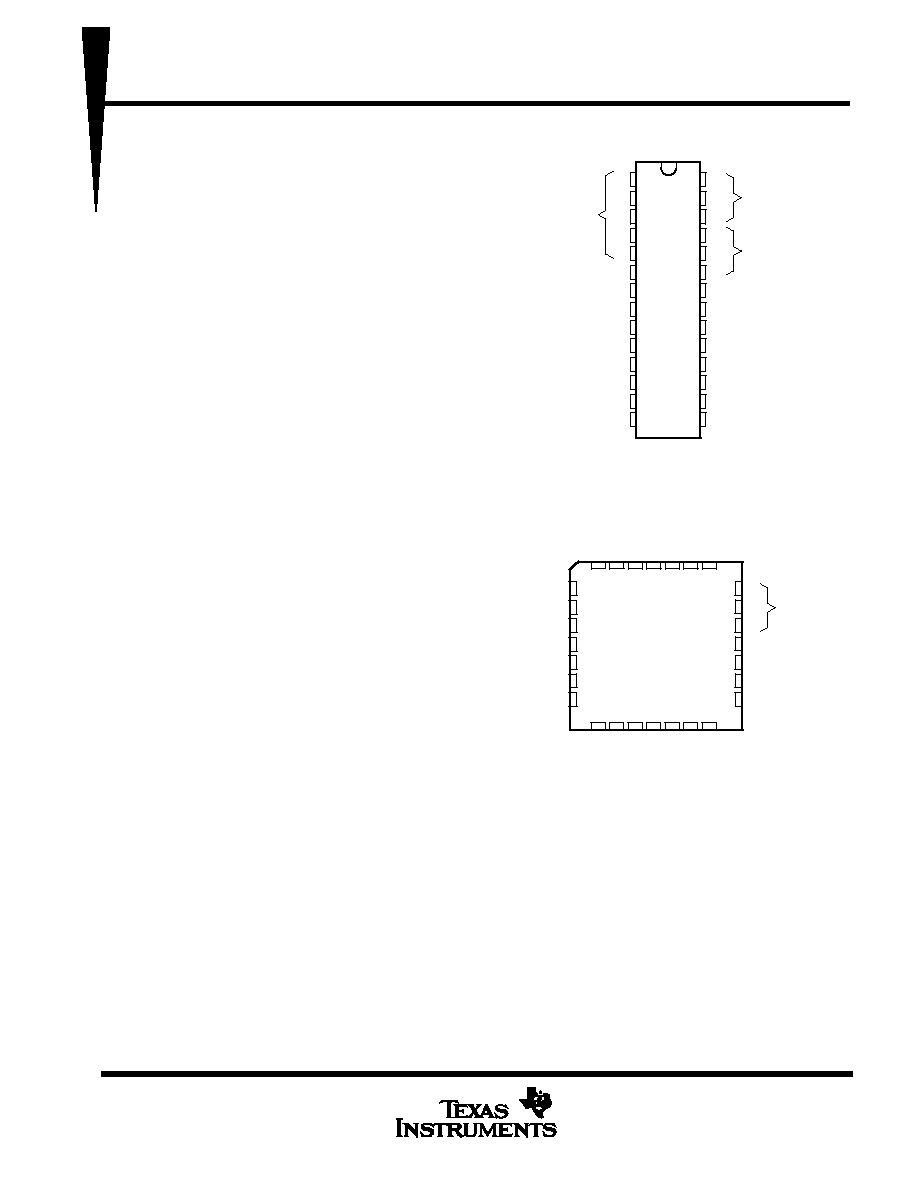
1
2
3
4
5
6
7
8
9
10
11
12
13
14
28
27
26
25
24
23
22
21
20
19
18
17
16
15
3
4
5
6
7
START
EOC
2
≠ 5
OEN
CLK
V
CC
REF+
GND
2
≠ 7
2
1
0
A
B
C
ALE
2
≠ 1
(MSB)
2
≠ 2
2
≠ 3
2
≠ 4
2
≠ 8
(LSB)
REF≠
2
≠ 6
J PACKAGE
(TOP VIEW)
INPUTS
ADDRESS
3 2 1
13 14
5
6
7
8
9
10
11
A
B
C
ALE
2
≠ 1
(MSB)
2
≠ 2
2
≠ 3
INPUT 7
START
EOC
2
≠ 5
OE
CLK
V
CC
4
15 16 17 18
GND
REF≠
INPUT
6
INPUT
5
INPUT
4
INPUT
3
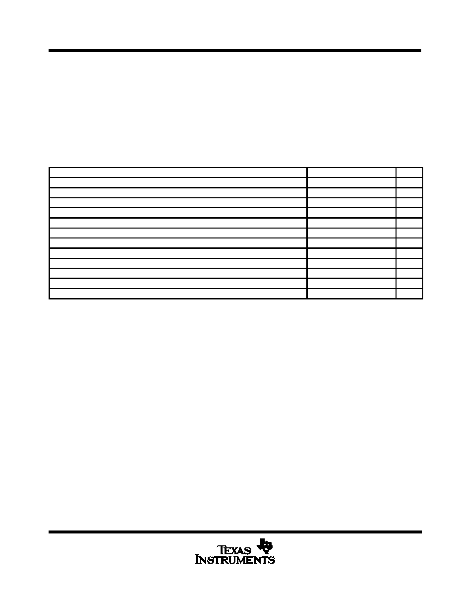
FK PACKAGE
(TOP VIEW)
28 27 26
25
24
23
22
21
20
19
12
REF+
INPUT
1
INPUT
0
INPUT
2
≠4
2
≠8
2
(LSB)
≠6
2
≠7
2
ADDRESS
INPUTS
PRODUCTION DATA information is current as of publication date.
Products conform to specifications per the terms of Texas Instruments
standard warranty. Production processing does not necessarily include
testing of all parameters.

ADC0808M
CMOS ANALOG-TO-DIGITAL CONVERTER
WITH 8-CHANNEL MULTIPLEXER
SGLS005A ≠ D2642, NOVEMBER 1986 ≠ REVISED MAY 1988
POST OFFICE BOX 655303
∑
DALLAS, TEXAS 75265
2
functional block diagram (positive logic)
2
8
21
20
19
18
15
14
17
7
EN
EOC
2≠1(MSB)
2≠2
2≠3
2≠4
2≠5
2≠6
2≠7
(LSB)
≠8
ALE
C
B
A
OEC
START
22
23
24
25
CLOCK
9
6
10
7
6
5
4
3
2
1
0
Decoder
Address
5
4
3
2
1
28
27
26
Detector
Threshold
Matrix
Switch
Capacitors
Binary-Weighted
16
12
REF≠
REF+
Sample-and-Hold
Timing
and
Control
Output
Latches
Digital
Outputs
Analog
Inputs
Analog
Multiplexor
MULTIPLEXER FUNCTION TABLE
INPUTS
SELECTED
ADDRESS
ADDRESS
ANALOG
C
B
A
STROBE
CHANNEL
L
L
L
0
L
L
H
1
L
H
L
2
L
H
H
3
H
L
L
4
H
L
H
5
H
H
L
6
H
H
H
7
H = high level, L = low level
= low-to-high transition

ADC0808M
CMOS ANALOG-TO-DIGITAL CONVERTER
WITH 8-CHANNEL MULTIPLEXER
SGLS005A ≠ D2642, NOVEMBER 1986 ≠ REVISED MAY 1988
POST OFFICE BOX 655303
∑
DALLAS, TEXAS 75265
3
operating sequence
Latch Outputs
OEN
(Internal)
Multiplex Output
INPUT
ADDRESS
START
CLK
Analog Value
Hi-Z State
10%
90%
10%
90%
50%
50%
tdis
tconv
50%
50%
Analog Value
Input Stable
tsu
th
50%
50%
Address Stable
w(ALC)
t
50%
50%
tw(S)
50%
50%
1/f
ten
ALE
EOC
td(EOC)
ADC0808M
CMOS ANALOG-TO-DIGITAL CONVERTER
WITH 8-CHANNEL MULTIPLEXER
SGLS005A ≠ D2642, NOVEMBER 1986 ≠ REVISED MAY 1988
POST OFFICE BOX 655303
∑
DALLAS, TEXAS 75265
4
absolute maximum ratings over operating free-air temperature range (unless otherwise noted)
Supply voltage, V
CC
(see Note 1)
6.5 V
. . . . . . . . . . . . . . . . . . . . . . . . . . . . . . . . . . . . . . . . . . . . . . . . . . . . . . . . . . .
Input voltage range: Control inputs
≠ 0.3 V to 15 V
. . . . . . . . . . . . . . . . . . . . . . . . . . . . . . . . . . . . . . . . . . . . . . . . . .
All other inputs
≠ 0.3 V to V
CC
+ 0.3 V
. . . . . . . . . . . . . . . . . . . . . . . . . . . . . . . . . . . . . . . . . .
Operating free-air temperature range
≠ 55
∞
C to 125
∞
C
. . . . . . . . . . . . . . . . . . . . . . . . . . . . . . . . . . . . . . . . . . . . . .
Storage temperature range
≠ 65
∞
C to 150
∞
C
. . . . . . . . . . . . . . . . . . . . . . . . . . . . . . . . . . . . . . . . . . . . . . . . . . . . . . .
Case temperature for 60 seconds: FK package
260
∞
C
. . . . . . . . . . . . . . . . . . . . . . . . . . . . . . . . . . . . . . . . . . . . . .
Lead temperature 1,6 mm (1/16 inch) from case for 60 seconds: J package
300
∞
C
. . . . . . . . . . . . . . . . . . . . .
NOTE 1: All voltage values are with respect to network ground terminal.
recommended operating conditions
MIN
NOM
MAX
UNIT
Supply voltage, VCC
4.5
5
6
V
Positive reference voltage, Vref + (see Note 2)
VCC
VCC + 0.1
V
Negative reference voltage, Vref ≠
0
≠ 0.1
V
Differential reference voltage, Vref + ≠ Vref ≠
5
V
High-level input voltage, VIH
VCC ≠ 1.5
V
Low-level input voltage, VIL
1.5
V
Start pulse duration, tw(S)
200
ns
Address load control pulse duration, tw(ALC)
200
ns
Address setup time, tsu
50
ns
Address hold time, th
50
ns
Clock frequency, fclock
10
640
1280
kHz
Operating free-air temperature, TA
≠ 55
125
∞
C
NOTE 2: Care must be taken that this rating is observed even during power-up.
ADC0808M
CMOS ANALOG-TO-DIGITAL CONVERTER
WITH 8-CHANNEL MULTIPLEXER
SGLS005A ≠ D2642, NOVEMBER 1986 ≠ REVISED MAY 1988
POST OFFICE BOX 655303
∑
DALLAS, TEXAS 75265
5
electrical characteristics over recommended operating free-air temperature range, V
CC
= 4.5 V to
5.5 V (unless otherwise noted)
total device
PARAMETER
TEST CONDITIONS
MIN
TYP
MAX
UNIT
VOH
High-level output voltage
IO = ≠360
µ
A
VCC ≠ 0.4
V
VOL
Low level output voltage
Data outputs
IO = 1.6 mA
0.45
V
VOL
Low-level output voltage
End of conversion
IO = 1.2 mA
0.45
V
IOZ
Off-state (high-impedance-state)
VO = VCC
3
µ
A
IOZ
output current
VO = 0
≠ 3
µ
A
II
Control input current at maiximum input voltage
VI = 15 V
1
µ
A
IIL
Low-level control input current
VI = 0
≠ 1
µ
A
ICC
Supply current
fclock = 640 kHz
0.3
3
mA
Ci
Input capacitance, control inputs
TA = 25
∞
C
10
pF
Co
Output capacitance, data outputs
TA = 25
∞
C
10
pF
Resistance from REF+ to REF ≠
1000
k
analog multiplexer
PARAMETER
TEST CONDITIONS
MIN
TYP
MAX
UNIT
I
Channel on state current (see Note 3)
VI = VCC,
fclock = 640 kHz
2
µ
A
Ion
Channel on-state current (see Note 3)
VI = 0,
fclock = 640 kHz
≠ 2
µ
A
VCC = 5 V,
VI = 5 V
10
200
nA
I ff
Channel off state current
TA = 25
∞
C
VI = 0
≠ 10
≠ 200
nA
Ioff
Channel off-state current
VCC = 5 V
VI = 5 V
1
µ
A
VCC = 5 V
VI = 0
≠ 1
µ
A
Typical values are at VCC = 5 V and TA = 25
∞
C.
NOTE 3: Channel on-state current is primarily due to the bias current into or out of the threshold detector, and it varies directly with clock frequency.
timing characteristics, V
CC
= V
ref+
= 5 V, V
ref≠
= 0 V, T
A
= 25
∞
C (unless otherwise noted)
PARAMETER
TEST CONDITIONS
MIN
TYP
MAX
UNIT
fclock
Clock frequency
10
640
1280
kHz
tconv
Conversion time
See Notes 4 and 5 and Figure 1
90
100
116
µ
s
tenH
Enable time, high
See Figure 1
150
360
ns
tenL
Enable time, low
See FIgure 1
90
25
ns
tdis
Output disable time
See Figure 1
200
405
ns
tw(s)
Pulse duration, START
200
ns
tw(ALE)
Pulse duration, ALE
200
ns
tsu
Setup time, ADDRESS
50
ns
th
Hold time, ADDRESS
50
ns
td(EOC)
Delay time, EOC
See Notes 4 and 6 and Figure 1
0
14.5
µ
s
NOTES: 4. Refer to the operating sequence diagram
5. For clock frequencies other than 640 kHz, tconv is 57 clock cycles minimum and 74 clock cycles maximum.
6. For clock frequencies other than 640 kHz, td(EOC) maximum is 8 clock cycles plus 2
µ
s.