 | ÐлекÑÑоннÑй компоненÑ: ADS1241 | СкаÑаÑÑ:  PDF PDF  ZIP ZIP |
Äîêóìåíòàöèÿ è îïèñàíèÿ www.docs.chipfind.ru
24-Bit
ANALOG-TO-DIGITAL CONVERTER
FEATURES
q
24 BITS NO MISSING CODES
q
SIMULTANEOUS 50Hz AND 60Hz REJECTION
(90dB MINIMUM)
q
0.0015% INL
q
21 BITS EFFECTIVE RESOLUTION
(PGA = 1), 19 BITS (PGA = 128)
q
PGA GAINS FROM 1 TO 128
q
SINGLE CYCLE SETTLING
q
PROGRAMMABLE DATA OUTPUT RATES
q
EXTERNAL DIFFERENTIAL REFERENCE
OF 0.1V TO 5V
q
ON-CHIP CALIBRATION
q
SPITM COMPATIBLE
q
2.7V TO 5.25V SUPPLY RANGE
q
600
µ
W POWER CONSUMPTION
q
UP TO EIGHT INPUT CHANNELS
q
UP TO EIGHT DATA I/O
DESCRIPTION
The ADS1240 and ADS1241 are precision, wide dynamic range,
delta-sigma, Analog-to-Digital (A/D) converters with 24-bit resolution
operating from 2.7V to 5.25V power supplies. The delta-sigma A/D
converter provides up to 24 bits of no missing code performance and
effective resolution of 21 bits.
The input channels are multiplexed. Internal buffering can be
selected to provide very high input impedance for direct connection
to transducers or low-level voltage signals. Burnout current sources
are provided that allow for detection of an open or shorted sensor.
An 8-bit Digital-to-Analog (D/A) converter provides an offset cor-
rection with a range of 50% of the Full-Scale Range (FSR).
The Programmable Gain Amplifier (PGA) provides selectable gains of
1 to 128, with an effective resolution of 19 bits at a gain of 128. The
A/D conversion is accomplished with a 2nd-order delta-sigma modu-
lator and programmable Finite-Impulse Response (FIR) filter that
provides a simultaneous 50Hz and 60Hz notch. The reference input
is differential and can be used for ratiometric conversion.
The serial interface is SPI compatible. Up to eight bits of data
I/O are also provided that can be used for input or output. The
ADS1240 and ADS1241 are designed for high-resolution measure-
ment applications in smart transmitters, industrial process control,
weigh scales, chromatography, and portable instrumentation.
APPLICATIONS
q
INDUSTRIAL PROCESS CONTROL
q
WEIGH SCALES
q
LIQUID /GAS CHROMATOGRAPHY
q
BLOOD ANALYSIS
q
SMART TRANSMITTERS
q
PORTABLE INSTRUMENTATION
BUF
PGA
A = 1:128
+
Clock Generator
Serial Interface
2nd-Order
Modulator
AGND
AV
DD
V
REF+
V
REF
X
IN
X
OUT
DSYNC
PDWN
RESET
DRDY
BUFEN
DGND
DV
DD
SCLK
POL
D
IN
D
OUT
CS
MUX
A
IN
0/D0
A
IN
1/D1
A
IN
2/D2
A
IN
3/D3
A
IN
4/D4
A
IN
5/D5
A
IN
6/D6
A
IN
7/D7
A
INCOM
Controller
Registers
Digital
Filter
2
µ
A
AV
DD
Offset
DAC
AGND
2
µ
A
ADS1241
Only
ADS1
241
ADS1
240
ADS1240
ADS1241
SBAS173C JUNE 2001 REVISED NOVEMBER 2003
www.ti.com
PRODUCTION DATA information is current as of publication date.
Products conform to specifications per the terms of Texas Instruments
standard warranty. Production processing does not necessarily include
testing of all parameters.
Copyright © 2001-2003, Texas Instruments Incorporated
Please be aware that an important notice concerning availability, standard warranty, and use in critical applications of
Texas Instruments semiconductor products and disclaimers thereto appears at the end of this data sheet.
All trademarks property of their respective owners.
ADS1240, 1241
2
SBAS173C
www.ti.com
SPECIFIED
PACKAGE
TEMPERATURE
PACKAGE
ORDERING
TRANSPORT
PRODUCT
PACKAGE-LEAD
DESIGNATOR
(1)
RANGE
MARKING
NUMBER
MEDIA, QUANTITY
ADS1240
SSOP-24
DB
40
°
C to +85
°
C
ADS1240E
ADS1240E
Rails, 60
"
"
"
"
"
ADS1240E/1K
Tape and Reel, 1000
ADS1241
SSOP-28
DB
40
°
C to +85
°
C
ADS1241E
ADS1241E
Rails, 48
"
"
"
"
"
ADS1241E/1K
Tape and Reel, 1000
DIGITAL CHARACTERISTICS: 40
°
C to +85
°
C, DV
DD
2.7V to 5.25V
PARAMETER
CONDITIONS
MIN
TYP
MAX
UNITS
Digital Input/Output
Logic Family
CMOS
Logic Level: V
IH
0.8 · DV
DD
DV
DD
V
V
IL
DGND
0.2 · DV
DD
V
V
OH
I
OH
= 1mA
DV
DD
0.4
V
V
OL
I
OL
= 1mA
DGND
DGND + 0.4
V
Input Leakage: I
IH
V
I
= DV
DD
10
µ
A
I
IL
V
I
= 0
10
µ
A
Master Clock Rate: f
OSC
1
5
MHz
Master Clock Period: t
OSC
1/f
OSC
200
1000
ns
AV
DD
to DGND ...................................................................... 0.3V to +6V
DV
DD
to DGND ...................................................................... 0.3V to +6V
Input Current ............................................................... 100mA, Momentary
DGND to AGND .................................................................... 0.3V to 0.3V
Input Current ................................................................. 10mA, Continuous
A
IN
................................................................. AGND 0.5V to AV
DD
+ 0.5V
Digital Input Voltage to DGND ................................. 0.3V to DV
DD
+ 0.3V
Digital Output Voltage to DGND .............................. 0.3V to DV
DD
+ 0.3V
Maximum Junction Temperature ................................................... +150
°
C
Operating Temperature Range ......................................... 40
°
C to +85
°
C
Storage Temperature Range .......................................... 60
°
C to +150
°
C
Lead Temperature (soldering, 10s) .............................................. +300
°
C
NOTE: (1) Stresses above these ratings may cause permanent damage.
Exposure to absolute maximum conditions for extended periods may degrade
device reliability.
ABSOLUTE MAXIMUM RATINGS
(1)
PACKAGE/ORDERING INFORMATION
NOTE: (1) For the most current specifications and package information, refer to our web site at www.ti.com.
EVALUATION MODULE ORDERING INFORMATION
PRODUCT
DESCRIPTION
ADS1241EVM
ADS1240 and ADS1241 Evaluation Module
ELECTROSTATIC
DISCHARGE SENSITIVITY
This integrated circuit can be damaged by ESD. Texas Instru-
ments recommends that all integrated circuits be handled with
appropriate precautions. Failure to observe proper handling
and installation procedures can cause damage.
ESD damage can range from subtle performance degradation
to complete device failure. Precision integrated circuits may be
more susceptible to damage because very small parametric
changes could cause the device not to meet its published
specifications.
ADS1240, 1241
3
SBAS173C
www.ti.com
ELECTRICAL CHARACTERISTICS: AV
DD
= 5V
All specifications T
MIN
to T
MAX
, AV
DD
= +5V, DV
DD
= +2.7V to 5.25V, f
MOD
= 19.2kHz, PGA = 1, Buffer ON, f
DATA
= 15Hz, and V
REF
= +2.5V, unless otherwise specified.
ADS1240
ADS1241
PARAMETER
CONDITIONS
MIN
TYP
MAX
UNITS
ANALOG INPUT (A
IN
0 A
IN
7, A
INCOM
)
Analog Input Range
Buffer OFF
AGND 0.1
AV
DD
+ 0.1
V
Buffer ON
AGND + 0.05
AV
DD
1.5
V
Full-Scale Input Range
(In+) (In), See Block Diagram, RANGE = 0
±
V
REF
/PGA
V
RANGE = 1
±
V
REF
/(2 · PGA)
V
Differential Input Impedance
Buffer OFF
5/PGA
M
Buffer ON
5
G
Bandwidth
f
DATA
= 3.75Hz
3dB
1.65
Hz
f
DATA
= 7.50Hz
3dB
3.44
Hz
f
DATA
= 15.00Hz
3dB
14.6
Hz
Programmable Gain Amplifier
User-Selectable Gain Ranges
1
128
Input Capacitance
9
pF
Input Leakage Current
Modulator OFF, T = 25
°
C
5
pA
Burnout Current Sources
2
µ
A
OFFSET DAC
Offset DAC Range
RANGE = 0
±
V
REF
/(2 · PGA)
V
RANGE = 1
±
V
REF
/(4 · PGA)
V
Offset Monotonicity
8
Bits
Offset DAC Gain Error
±
10
%
Offset DAC Gain Error Drift
1
ppm/
°
C
SYSTEM PERFORMANCE
Resolution
No Missing Codes
24
Bits
Integral Nonlinearity
End Point Fit
±
0.0015
% of FS
Offset Error
(1)
7.5
ppm of FS
Offset Drift
(1)
0.02
ppm of FS/
°
C
Gain Error
0.005
%
Gain Error Drift
(1)
0.5
ppm/
°
C
Common-Mode Rejection
at DC
100
dB
f
CM
= 60Hz, f
DATA
= 15Hz
130
dB
f
CM
= 50Hz, f
DATA
= 15Hz
120
dB
Normal-Mode Rejection
f
SIG
= 50Hz, f
DATA
= 15Hz
100
dB
f
SIG
= 60Hz, f
DATA
= 15Hz
100
dB
Output Noise
See Typical Characteristics
Power-Supply Rejection
at DC, dB = 20 log(
V
OUT
/
V
DD
)
(2)
80
95
dB
VOLTAGE REFERENCE INPUT
V
REF
V
REF
(REF IN+) (REF IN), RANGE = 0
0.1
2.5
2.6
V
Reference Input Range
REF IN+, REF IN
0
AV
DD
V
RANGE = 1
0.1
AV
DD
V
Common-Mode Rejection
at DC
120
dB
Common-Mode Rejection
f
VREFCM
= 60Hz, f
DATA
= 15Hz
120
dB
Bias Current
(3)
V
REF
= 2.5V
1.3
µ
A
POWER-SUPPLY REQUIREMENTS
Power-Supply Voltage
AV
DD
4.75
5.25
V
Analog Current
PDWN = 0, or SLEEP
1
nA
PGA = 1, Buffer OFF
120
250
µ
A
PGA = 128, Buffer OFF
400
675
µ
A
PGA = 1, Buffer ON
160
300
µ
A
PGA = 128, Buffer ON
760
1275
µ
A
Digital Current
Normal Mode, DV
DD
= 5V
80
125
µ
A
SLEEP Mode, DV
DD
= 5V
60
µ
A
Read Data Continuous Mode, DV
DD
= 5V
230
µ
A
PDWN
0.5
nA
Power Dissipation
PGA = 1, Buffer OFF, DV
DD
= 5V
1.1
1.9
mW
NOTES: (1) Calibration can minimize these errors to the level of the noise.
(2)
V
OUT
is a change in digital result.
(3) 12pF switched capacitor at f
SAMP
clock frequency.
ADS1240, 1241
4
SBAS173C
www.ti.com
ELECTRICAL CHARACTERISTICS: AV
DD
= 3V
All specifications 40
°
C to +85
°
C, AV
DD
= +3V, DV
DD
= +2.7V to 5.25V, f
MOD
= 19.2kHz, PGA = 1, Buffer ON, f
DATA
= 15Hz, and V
REF
= +1.25V, unless otherwise specified.
ADS1240
ADS1241
PARAMETER
CONDITIONS
MIN
TYP
MAX
UNITS
ANALOG INPUT (A
IN
0 A
IN
7, A
INCOM
)
Analog Input Range
Buffer OFF
AGND 0.1
AV
DD
+ 0.1
V
Buffer ON
AGND + 0.05
AV
DD
1.5
V
Full-Scale Input Voltage Range
(In+) (In) See Block Diagram, RANGE = 0
±
V
REF
/PGA
V
RANGE = 1
±
V
REF
/(2 · PGA)
V
Input Impedance
Buffer OFF
5/PGA
M
Differential
Buffer ON
5
G
Bandwidth
f
DATA
= 3.75Hz
3dB
1.65
Hz
f
DATA
= 7.50Hz
3dB
3.44
Hz
f
DATA
= 15.00Hz
3dB
14.6
Hz
Programmable Gain Amplifier
User-Selectable Gain Ranges
1
128
Input Capacitance
9
pF
Input Leakage Current
Modulator OFF, T = 25
°
C
5
pA
Burnout Current Sources
2
µ
A
OFFSET DAC
Offset DAC Range
RANGE = 0
±
V
REF
/(2 · PGA)
V
RANGE = 1
±
V
REF
/(4 · PGA)
V
Offset DAC Monotonicity
8
Bits
Offset DAC Gain Error
±
10
%
Offset DAC Gain Error Drift
2
ppm/
°
C
SYSTEM PERFORMANCE
Resolution
No Missing Codes
24
Bits
Integral Nonlinearity
End Point Fit
±
0.0015
% of FS
Offset Error
(1)
15
ppm of FS
Offset Drift
(1)
0.04
ppm of FS/
°
C
Gain Error
0.01
%
Gain Error Drift
(1)
1.0
ppm/
°
C
Common-Mode Rejection
at DC
100
dB
f
CM
= 60Hz, f
DATA
= 15Hz
130
dB
f
CM
= 50Hz, f
DATA
= 15Hz
120
dB
Normal-Mode Rejection
f
SIG
= 50Hz, f
DATA
= 15Hz
100
dB
f
SIG
= 60Hz, f
DATA
= 15Hz
100
dB
Output Noise
See Typical Characteristics
Power-Supply Rejection
at DC, dB = 20 log(
V
OUT
/
V
DD
)
(2)
75
90
dB
VOLTAGE REFERENCE INPUT
V
REF
V
REF
(REF IN+) (REF IN), RANGE = 0
0.1
1.25
1.30
V
Reference Input Range
REF IN+, REF IN
0
AV
DD
V
RANGE = 1
0.1
2.5
2.6
V
Common-Mode Rejection
at DC
120
dB
Common-Mode Rejection
f
VREFCM
= 60Hz, f
DATA
= 15Hz
120
dB
Bias Current
(3)
V
REF
= 1.25
0.65
µ
A
POWER-SUPPLY REQUIREMENTS
Power-Supply Voltage
AV
DD
2.7
3.3
V
Analog Current
PDWN = 0, or SLEEP
1
nA
PGA = 1, Buffer OFF
107
225
µ
A
PGA = 128, Buffer OFF
355
600
µ
A
PGA = 1, Buffer ON
118
275
µ
A
PGA = 128, Buffer ON
483
1225
µ
A
Digital Current
Normal Mode, DV
DD
= 3V
50
100
µ
A
SLEEP Mode, DV
DD
= 3V
40
µ
A
Read Data Continuous Mode, DV
DD
= 3V
113
µ
A
PDWN = 0
0.5
nA
Power Dissipation
PGA = 1, Buffer OFF, DV
DD
= 3V
0.6
1.2
mW
NOTES: (1) Calibration can minimize these errors to the level of the noise.
(2)
V
OUT
is a change in digital result.
(3) 12pF switched capacitor at f
SAMP
clock frequency.
ADS1240, 1241
5
SBAS173C
www.ti.com
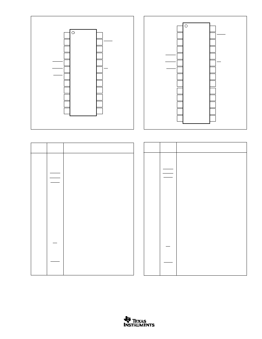
PIN CONFIGURATION (ADS1240)
PIN
NUMBER
NAME
DESCRIPTION
1
DV
DD
Digital Power Supply
2
DGND
Digital Ground
3
X
IN
Clock Input
4
X
OUT
Clock Output, used with external crystals.
5
RESET
Active LOW, resets the entire device.
6
DSYNC
Active LOW, Synchronization Control
7
PDWN
Active LOW, Power Down. The power down func-
tion shuts down the analog and digital circuits.
8
DGND
Digital Ground
9
V
REF+
Positive Differential Reference Input
10
V
REF
Negative Differential Reference Input
11
A
IN
0/D0
Analog Input 0 / Data I/O 0
12
A
IN
1/D1
Analog Input 1 / Data I/O 1
13
A
IN
2/D2
Analog Input 2 / Data I/O 2
14
A
IN
3/D3
Analog Input 3 / Data I/O 3
15
A
INCOM
Analog Input Common, connect to AGND if unused.
16
AGND
Analog Ground
17
AV
DD
Analog Power Supply
18
POL
Serial Clock Polarity
19
CS
Active LOW, Chip Select
20
D
IN
Serial Data Input, Schmitt Trigger
21
D
OUT
Serial Data Output
22
SCLK
Serial Clock, Schmitt Trigger
23
DRDY
Active LOW, Data Ready
24
BUFEN
Buffer Enable
PIN DESCRIPTIONS (ADS1240)
ADS1240
1
2
3
4
5
6
7
8
9
10
11
12
24
23
22
21
20
19
18
17
16
15
14
13
DV
DD
DGND
X
IN
X
OUT
RESET
DSYNC
PDWN
DGND
V
REF+
V
REF
A
IN
0/D0
A
IN
1/D1
BUFEN
DRDY
SCLK
D
OUT
D
IN
CS
POL
AV
DD
AGND
A
INCOM
A
IN
3/D3
A
IN
2/D2
PIN CONFIGURATION (ADS1241)
ADS1241
1
2
3
4
5
6
7
8
9
10
11
12
13
14
28
27
26
25
24
23
22
21
20
19
18
17
16
15
DV
DD
DGND
X
IN
X
OUT
RESET
DSYNC
PDWN
DGND
V
REF+
V
REF
A
IN
0/D0
A
IN
1/D1
A
IN
4/D4
A
IN
5/D5
BUFEN
DRDY
SCLK
D
OUT
D
IN
CS
POL
AV
DD
AGND
A
INCOM
A
IN
3/D3
A
IN
2/D2
A
IN
7/D7
A
IN
6/D6
PIN
NUMBER
NAME
DESCRIPTION
1
DV
DD
Digital Power Supply
2
DGND
Digital Ground
3
X
IN
Clock Input
4
X
OUT
Clock Output, used with external crystals.
5
RESET
Active LOW, resets the entire device.
6
DSYNC
Active LOW, Synchronization Control
7
PDWN
Active LOW, Power Down. The power down func-
tion shuts down the analog and digital circuits.
8
DGND
Digital Ground
9
V
REF+
Positive Differential Reference Input
10
V
REF
Negative Differential Reference Input
11
A
IN
0/D0
Analog Input 0 / Data I/O 0
12
A
IN
1/D1
Analog Input 1 / Data I/O 1
13
A
IN
4/D4
Analog Input 4 / Data I/O 4
14
A
IN
5/D5
Analog Input 5 / Data I/O 5
15
A
IN
6/D6
Analog Input 6 / Data I/O 6
16
A
IN
7/D7
Analog Input 7 / Data I/O 7
17
A
IN
2/D2
Analog Input 2 / Data I/O 2
18
A
IN
3/D3
Analog Input 3 / Data I/O 3
19
A
INCOM
Analog Input Common, connect to AGND if unused.
20
AGND
Analog Ground
21
AV
DD
Analog Power Supply
22
POL
Serial Clock Polarity
23
CS
Active LOW, Chip Select
24
D
IN
Serial Data Input, Schmitt Trigger
25
D
OUT
Serial Data Output
26
SCLK
Serial Clock, Schmitt Trigger
27
DRDY
Active LOW, Data Ready
28
BUFEN
Buffer Enable
PIN DESCRIPTIONS (ADS1241)
Top View
SSOP
Top View
SSOP
Document Outline
- FEATURES
- APPLICATIONS
- DESCRIPTION
- ABSOLUTE MAXIMUM RATINGS(
- EVALUATION MODULE ORDERING INFORMATION
- PACKAGE/ORDERING INFORMATION
- DIGITAL CHARACTERISTICS:
40°C to +85°C, DVDD 2.7V to 5.25V
- ELECTRICAL CHARACTERISTICS: AVDD = 5V
- ELECTRICAL CHARACTERISTICS: AVDD = 3V
- PIN CONFIGURATION (ADS1240)
- PIN DESCRIPTIONS (ADS1240)
- PIN CONFIGURATION (ADS1241)
- PIN DESCRIPTIONS (ADS1241)
- TIMING DIAGRAMS
- TIMING CHARACTERISTICS TABLES
- TYPICAL CHARACTERISTICS
- OVERVIEW
- INPUT MULTIPLEXER
- BURNOUT CURRENT SOURCES
- INPUT BUFFER
- PGA
- OFFSET DAC
- MODULATOR
- CALIBRATION
- EXTERNAL VOLTAGE REFERENCE
- CLOCK GENERATOR
- DIGITAL FILTER
- DATA I/O INTERFACE
- SERIAL PERIPHERAL INTERFACE
- Chip Select (CS)\
- Serial Clock (SCLK)
- Clock Polarity (POL)
- Data Input ( DIN) and Data Output (DOUT)
- DATA READY DRDY\ PIN
- DSYNC OPERATION
- POWER-UPÛSUPPLY VOLTAGE RAMP RATE
- RESET
- ADS1240 AND ADS1241 REGISTER
- DETAILED REGISTER DEFINITIONS
- ADS1240 AND ADS1241 CONTROL COMMAND DEFINITIONS
- RDATA-Read Data
- RDATAC-Read Data Continuous
- STOPC-Stop Continuous
- RREG-Read from Registers
- WREG-Write to Registers
- SELFCAL-Offset and Gain Self Calibration
- SELFOCAL-Offset Self Calibration
- SELFGCAL-Gain Self Calibration
- SYSOCAL-System Offset Calibration
- SYSGCAL-System Gain Calibration
- WAKEUP
- DSYNC-Sync DRDY\
- SLEEP-Sleep Mode
- RESET-Reset to Default Values
- APPLICATION EXAMPLES
- GENERAL-PURPOSE WEIGH SCALE
- HIGH PRECISION WEIGH SCALE
- DEFINITION OF TERMS
- IMPORTANT NOTICE