 | ÐлекÑÑоннÑй компоненÑ: ADS7815 | СкаÑаÑÑ:  PDF PDF  ZIP ZIP |
16-Bit 250kHz Sampling CMOS Analog-to-Digital Converter
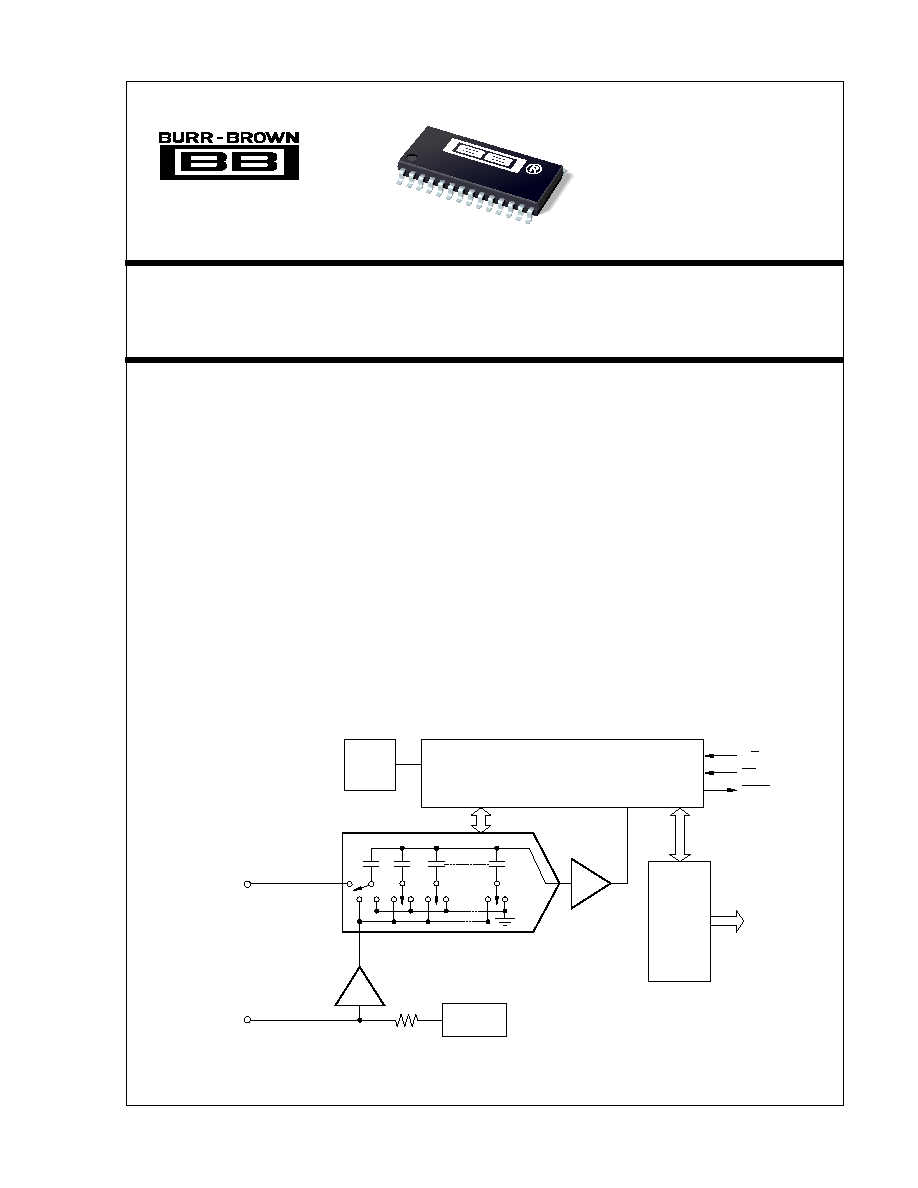
16-Bit 250kHz Sampling CMOS
ANALOG-to-DIGITAL CONVERTER
DESCRIPTION
The ADS7815 is a complete 16-bit sampling analog-
to-digital (A/D) converter featuring excellent AC
performance and a 250kHz throughput rate. The de-
sign includes a 16-bit capacitor-based SAR A/D
converter with an inherent sample and hold (S/H), a
precision reference, and an internal clock. Spurious-
free dynamic range with a 100kHz full-scale sinewave
input is typically greater than 100dB. The
±
2.5V input
range allows development of precision systems using
only
±
5V supplies. The converter is available in a
28-lead SOIC package specified for operation over
the industrial 25
°
C to +85
°
C temperature range.
ADS7815
®
FEATURES
q
250kHz SAMPLING RATE
q
COMPLETE WITH S/H, REF, CLOCK, ETC.
q
96dB min SFDR WITH 100kHz INPUT
q
84dB min SINAD
q
±
2.5V INPUT RANGE
q
28-LEAD SOIC
CDAC
Output
Latches
and
Three
State
Drivers
Comparator
Buffer
5k
REF Out/In
±2.5V Input
Successive Approximation Register and Control Logic
Clock
BUSY
CS
R/C
Internal
+2.5V Ref
Parallel
Data
Bus
©
1996 Burr-Brown Corporation
PDS-1364A
Printed in U.S.A. December, 1996
International Airport Industrial Park · Mailing Address: PO Box 11400, Tucson, AZ 85734 · Street Address: 6730 S. Tucson Blvd., Tucson, AZ 85706 · Tel: (520) 746-1111 · Twx: 910-952-1111
Internet: http://www.burr-brown.com/ · FAXLine: (800) 548-6133 (US/Canada Only) · Cable: BBRCORP · Telex: 066-6491 · FAX: (520) 889-1510 · Immediate Product Info: (800) 548-6132
APPLICATIONS
q
WIRELESS BASE STATIONS
q
SPECTRUM ANALYSIS
q
IMAGING SYSTEMS
q
DATA ACQUISITION
ADS7815
SBAS065

®
ADS7815
2
RESOLUTION
16
Bits
ANALOG INPUT
Voltage Range
±
2.5V
V
Impedance
100
M
Capacitance
30
pF
THROUGHPUT SPEED
Conversion Cycle
Acquire and Convert
4.0
µ
s
Throughput Rate
250
kHz
DC ACCURACY
Integral Linearity Error
±
4
LSB
(1)
No Missing Codes
15
Bits
Transition Noise
(2)
0.8
LSB
Full Scale Error
(3)
±
0.1
%
Full Scale Error Drift
±
7
ppm/
°
C
Bipolar Zero Error
±
2
mV
Bipolar Zero Error Drift
±
2
ppm/
°
C
Power Supply Sensitivity
+V
S
±
5%, V
S
±
5%
±
6
LSB
AC ACCURACY
Spurious-Free Dynamic Range
f
IN
= 100kHz
96
100
dB
(4)
Total Harmonic Distortion
f
IN
= 100kHz
98
96
dB
Signal-to-(Noise+Distortion)
f
IN
= 100kHz
84
dB
60dB Input
28
dB
Signal-to-Noise
f
IN
= 100kHz
84
dB
Usable Bandwidth
(5)
1
MHz
Aperture Delay
40
ns
REFERENCE
Internal Reference Voltage
2.45
2.5
2.55
V
Internal Reference Source Current
1
µ
A
External Reference Voltage Range
2.3
2.5
2.7
V
External Reference Current Drain
V
REF
= +2.5V
100
µ
A
DIGITAL INPUTS
Logic Levels
V
IL
0.3
+0.8
V
V
IH
+2.8
+V
S
+0.3V
V
I
IL
±
10
µ
A
I
IH
±
10
µ
A
DIGITAL OUTPUTS
Data Format
Data Coding
V
OL
I
SINK
= 1.6mA
+0.4
V
V
OH
I
SOURCE
= 200
µ
A
+4
V
Leakage Current
High-Z State,
±
5
µ
A
V
OUT
= 0V to V
DIG
Output Capacitance
High-Z State
15
pF
DIGITAL TIMING
Bus Access Time
83
ns
Bus Relinquish Time
83
ns
POWER SUPPLIES
+V
S
+4.75
+5
+5.25
V
V
S
5.25
5
4.75
V
+I
S
+30
mA
I
S
10
mA
Power Dissipation
200
250
mW
TEMPERATURE RANGE
Specified Performance
25
+85
°
C
Storage
55
+125
°
C
NOTES: (1) LSB means Least Significant Bit. For the 16-bit,
±
2.5V input ADS7815, one LSB is 76
µ
V. (2) Typical rms noise at worst case transitions and
temperatures. (3) Full scale error is the worst case of Full Scale or +Full Scale untrimmed deviation from ideal first and last code transitions, divided by the transition
voltage (not divided by the full-scale range) and includes the effect of offset error. (4) All specifications in dB are referred to a full-scale
±
2.5V input. (5) Full-Power
Bandwidth defined as Full-Scale input frequency at which Signal-to-(Noise+Distortion) degrades to 60dB, or 10 bits of accuracy.
SPECIFICATIONS
At T
A
= 25
°
C to +85
°
C, f
S
= 250kHz, +V
S
= +5V, and V
S
= 5V, using internal reference, unless otherwise specified.
ADS7815U
PARAMETER
CONDITIONS
MIN
TYP
MAX
UNITS
Parallel 16 bits
Binary Two's Complement
®
ADS7815
3
The information provided herein is believed to be reliable; however, BURR-BROWN assumes no responsibility for inaccuracies or omissions. BURR-BROWN
assumes no responsibility for the use of this information, and all use of such information shall be entirely at the user's own risk. Prices and specifications are subject
to change without notice. No patent rights or licenses to any of the circuits described herein are implied or granted to any third party. BURR-BROWN does not
authorize or warrant any BURR-BROWN product for use in life support devices and/or systems.
ABSOLUTE MAXIMUM RATINGS
Analog Inputs: V
IN
................................................................................
±
V
S
REF ............................................ GND 0.3V to +V
S
+0.3V
CAP ............................................... Indefinite Short to GND
Momentary Short to +V
S
+V
S
......................................................................................................... 7V
V
S
...................................................................................................... 7V
Digital Inputs ...................................................... GND 0.3V to +V
S
+0.3V
Maximum Junction Temperature ................................................... +165
°
C
Internal Power Dissipation ............................................................. 825mW
Lead Temperature (soldering, 10s) ................................................ +300
°
C
ELECTROSTATIC
DISCHARGE SENSITIVITY
This integrated circuit can be damaged by ESD. Burr-Brown
recommends that all integrated circuits be handled with
appropriate precautions. Failure to observe proper handling
and installation procedures can cause damage.
ESD damage can range from subtle performance degradation
to complete device failure. Precision integrated circuits may
be more susceptible to damage because very small parametric
changes could cause the device not to meet its published
specifications.
PACKAGE
DRAWING
TEMPERATURE
PRODUCT
PACKAGE
NUMBER
(1)
RANGE
ADS7815U
28-Pin SOIC
217
25
°
C to +85
°
C
NOTE: (1) For detailed drawing and dimension table, please see end of data
sheet, or Appendix C of Burr-Brown IC Data Book.
PACKAGE/ORDERING INFORMATION
®
ADS7815
4
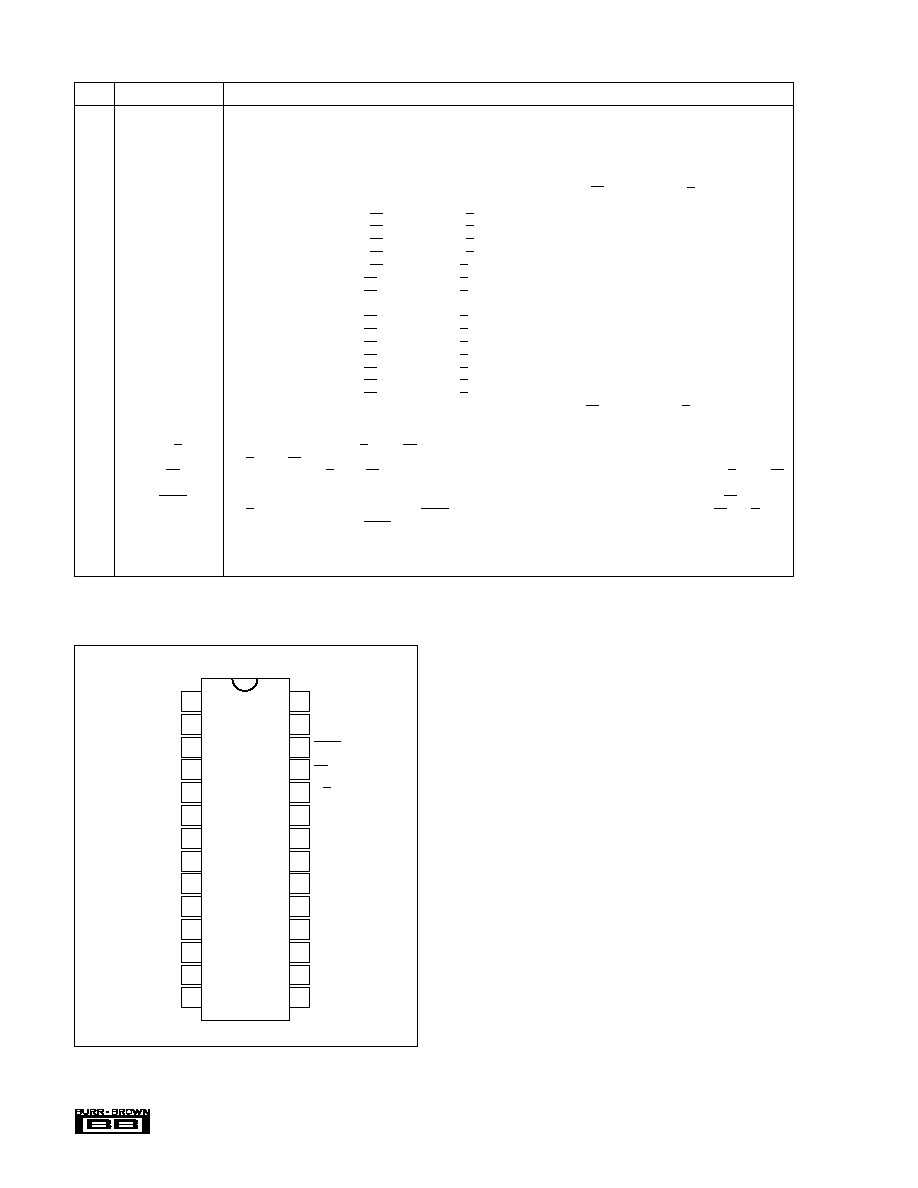
PIN #
NAME
DESCRIPTION
1
V
IN
Analog Input. Full-scale input range is
±
2.5V.
2
GND
Ground.
3
REF
Reference Input/Output. Outputs internal reference of +2.5V nominal. Can also be driven by external system reference. In
both cases, connect to ground with a 0.1
µ
F ceramic capacitor in parallel with 2.2
µ
F tantalum capacitor.
4
CAP
Reference compensation capacitor. Use a parallel combination of a 0.1
µ
F ceramic capacitor and a 2.2
µ
F tantalum capacitor.
5
GND
Ground.
6
D15 (MSB)
Data Bit 15. Most Significant Bit (MSB) of conversion results. Hi-Z state when CS is HIGH, when R/C is LOW or when a
conversion is in progress.
7
D14
Data Bit 14. Hi-Z state when CS is HIGH, when R/C is LOW or when a conversion is in progress.
8
D13
Data Bit 13. Hi-Z state when CS is HIGH, when R/C is LOW or when a conversion is in progress.
9
D12
Data Bit 12. Hi-Z state when CS is HIGH, when R/C is LOW or when a conversion is in progress.
10
D11
Data Bit 11. Hi-Z state when CS is HIGH, when R/C is LOW or when a conversion is in progress.
11
D10
Data Bit 10. Hi-Z state when CS is HIGH, when R/C is LOW or when a conversion is in progress.
12
D9
Data Bit 9. Hi-Z state when CS is HIGH, when R/C is LOW or when a conversion is in progress.
13
D8
Data Bit 8. Hi-Z state when CS is HIGH, when R/C is LOW or when a conversion is in progress.
14
GND
Ground.
15
D7
Data Bit 7. Hi-Z state when CS is HIGH, when R/C is LOW or when a conversion is in progress.
16
D6
Data Bit 6. Hi-Z state when CS is HIGH, when R/C is LOW or when a conversion is in progress.
17
D5
Data Bit 5. Hi-Z state when CS is HIGH, when R/C is LOW or when a conversion is in progress.
18
D4
Data Bit 4. Hi-Z state when CS is HIGH, when R/C is LOW or when a conversion is in progress.
19
D3
Data Bit 3. Hi-Z state when CS is HIGH, when R/C is LOW or when a conversion is in progress.
20
D2
Data Bit 2. Hi-Z state when CS is HIGH, when R/C is LOW or when a conversion is in progress.
21
D1
Data Bit 1. Hi-Z state when CS is HIGH, when R/C is LOW or when a conversion is in progress.
22
D0 (LSB)
Data Bit 0. Least Significant Bit (LSB) of conversion results. Hi-Z state when CS is HIGH, when R/C is LOW or when a
conversion is in progress.
23
V
S
Negative supply input. Nominally 5V. Decouple to analog ground with 0.1
µ
F ceramic and 10
µ
F tantalum capacitors.
24
R/C
Read/convert input. With R/C HIGH, CS going LOW will enable the output data bits if a conversion is not in progress. With
R/C LOW, CS going LOW will start a conversion if one is not already in progress.
25
CS
Chip select. With R/C LOW, CS going LOW will initiate a conversion if one is not already in progress. With R/C HIGH, CS
going LOW will enable the output data bits if a conversion is not in progress.
26
BUSY
Busy output. Falls when a conversion is started, and remains LOW until the conversion is completed. With CS LOW and
R/C HIGH, output data will be valid when BUSY rises, so that the rising edge can be used to latch the data. CS or R/C must
be HIGH within 250ns after BUSY rises or another conversion will start without time for signal acquisition.
27
+V
S
Positive supply input. Nominally +5V. Connect directly to pin 28.
28
+V
S
Positive supply input. Nominally +5V. Connect directly to pin 27. Decouple to ground with 0.1
µ
F ceramic and 10
µ
F
tantalum capacitors.
TABLE I. Pin Assignments.
PIN CONFIGURATION
Top View
SOIC
+V
S
+V
S
BUSY
CS
R/C
V
S
D0 (LSB)
D1
D2
D3
D4
D5
D6
D7
V
IN
GND
REF
CAP
GND
D15 (MSB)
D14
D13
D12
D11
D10
D9
D8
GND
1
2
3
4
5
6
7
8
9
10
11
12
13
14
28
27
26
25
24
23
22
21
20
19
18
17
16
15
ADS7815
®
ADS7815
5
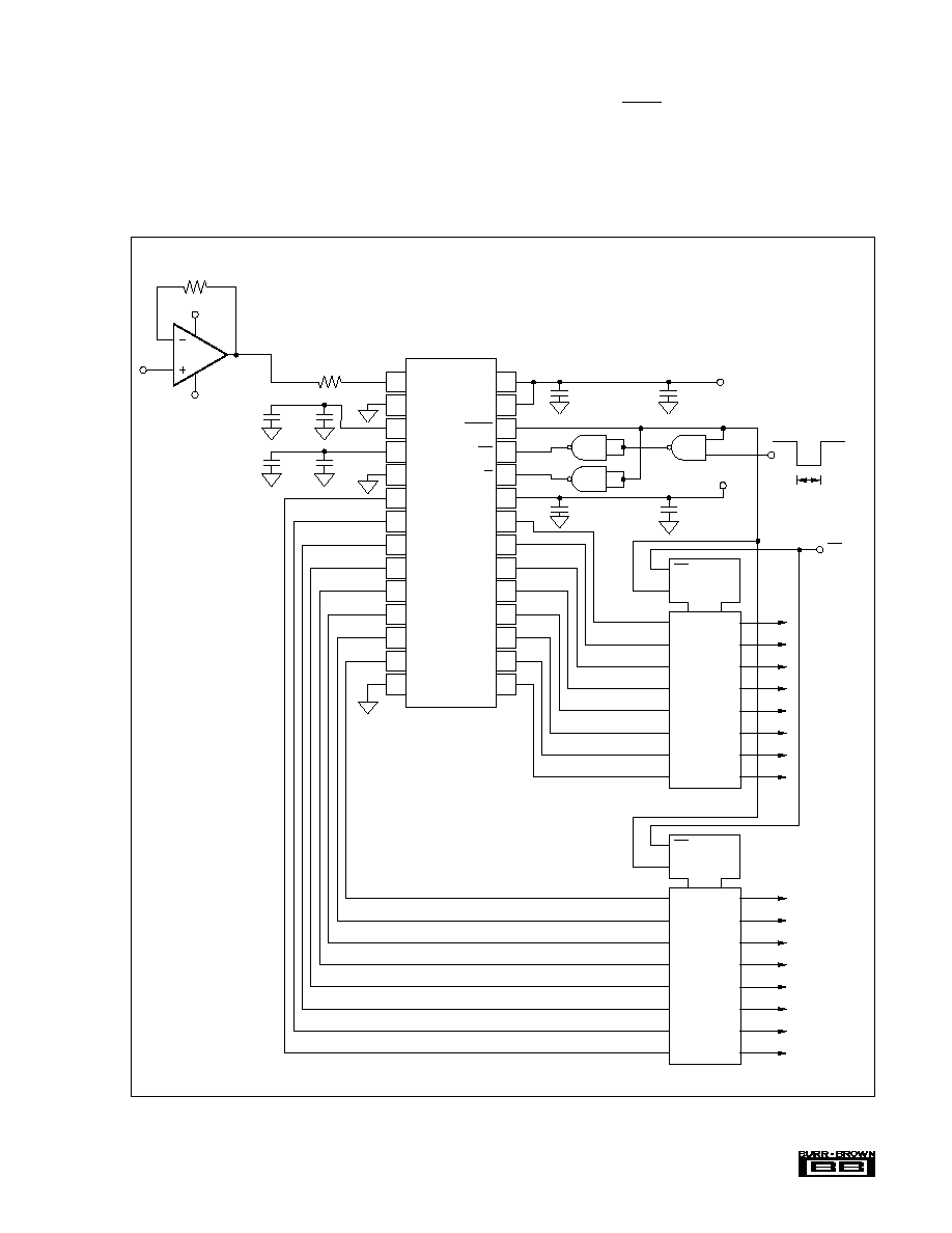
BASIC OPERATION
Figure 1 shows the recommended circuit for operation of the
ADS7815. A falling edge on the convert pulse signal places
the sample and hold into the hold mode and initiates a
conversion. When the conversion is complete, the pins D15
through D0 become active and the result of the conversion
is placed on these outputs. In the circuit shown in Figure 1,
the rising edge of BUSY latches the result into the 74HC574s.
After the conversion is complete, the ADS7815 sample and
hold returns to the sample mode and begins acquiring the
input signal for the next conversion. Allowing 4
µ
s between
falling edges of the convert pulse signal assures accurate
acquisition of the analog input.
FIGURE 1. Basic Operation.
1
2
3
4
5
6
7
8
9
10
11
12
13
14
V
IN
GND
REF
CAP
GND
D15
D14
D13
D12
D11
D10
D9
D8
GND
28
27
26
25
24
23
22
21
20
19
18
17
16
15
+V
S
+V
S
BUSY
CS
R/C
V
S
D0
D1
D2
D3
D4
D5
D6
D7
ADS7815
R
1
75
+5V
5V
+
2.2µF
C
4
0.1µF
C
6
+
2.2µF
C
3
0.1µF
C
5
Convert Pulse
74HC00
100ns min
µProcessor
Bus
µProcessor
Bus
+5V
0.1µF
C
1
+
10µF
C
2
5V
OC
0.1µF
C
7
+
10µF
C
8
2
3
4
5
6
7
8
9
1D
2D
3D
4D
5D
6D
7D
8D
1Q
2Q
3Q
4Q
5Q
6Q
7Q
8Q
1
10
OC
CLK
74HC574
2
3
4
5
6
7
8
9
1D
2D
3D
4D
5D
6D
7D
8D
1Q
2Q
3Q
4Q
5Q
6Q
7Q
8Q
1
10
OC
CLK
74HC574
R
2
10
OPA628