 | –≠–ª–µ–∫—Ç—Ä–æ–Ω–Ω—ã–π –∫–æ–º–ø–æ–Ω–µ–Ω—Ç: ADS7870 | –°–∫–∞—á–∞—Ç—å:  PDF PDF  ZIP ZIP |
1
Æ
ADS7870
Æ
ADS7870
©
1999 Burr-Brown Corporation
PDS-1539A
Printed in U.S.A. December, 1999
FEATURES
q
16-BIT DYNAMIC RANGE
q
PGA GAINS: 1, 2, 4, 5, 8, 10, 16, 20V/V
q
4-CHANNEL DIFFERENTIAL/8-CHANNEL
SINGLE ENDED MULTIPLEXER
q
2.048V OR 2.5V INTERNAL REFERENCE
q
FAST SERIAL INTERFACE
q
HIGH THROUGHPUT RATE: 52ksamples/s
q
ERROR/OVERLOAD INDICATOR
q
2.7V TO 5.5V SINGLE-SUPPLY OPERATION
q
4-BIT DIGITAL I/O VIA SERIAL INTERFACE
q
SSOP-28 PACKAGE
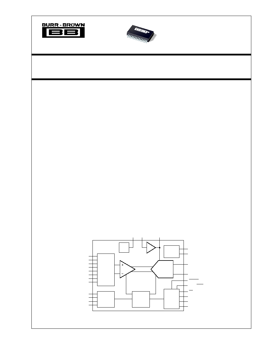
12-Bit ADC, MUX, PGA and Internal Reference
DATA ACQUISITION SYSTEM
DESCRIPTION
The ADS7870
(1)
is a complete low-power data acquisi-
tion system on a single chip. It consists of a 4-channel
differential/8-channel single-ended multiplexer, preci-
sion programmable gain amplifier, 12-bit successive
approximation analog-to-digital converter and a preci-
sion voltage reference.
The programmable-gain amplifier provides high input
impedance, excellent gain accuracy, good common-
mode rejection, and low noise.
For many low-level signals, no external amplification or
impedance buffering is needed between the signal
source and the A/D input.
APPLICATIONS
q
PORTABLE/BATTERY POWERED
SYSTEMS
q
LOW POWER INSTRUMENTATION
q
LOW POWER CONTROL SYSTEMS
q
SMART SENSOR APPLICATIONS
International Airport Industrial Park ∑ Mailing Address: PO Box 11400, Tucson, AZ 85734 ∑ Street Address: 6730 S. Tucson Blvd., Tucson, AZ 85706 ∑ Tel: (520) 746-1111
Twx: 910-952-1111 ∑ Internet: http://www.burr-brown.com/ ∑ Cable: BBRCORP ∑ Telex: 066-6491 ∑ FAX: (520) 889-1510 ∑ Immediate Product Info: (800) 548-6132
ADS7870
REF
Serial
Interface
ADS7870
DIN
SCLK
CS
CONVERT
RESET
RISE/FALL
BUSY
DOUT
Clock
Divider
Oscillator
OSC ENABLE
CCLK
BUF
OUT
/REF
IN
BUF
IN
V
REF
12-Bit
A/D
BUF
MUX
8 Ch
(4 Ch Diff.)
Analog
Inputs
Digital
I/O
Registers
and
Control
I/O 0
I/O 1
I/O 2
I/O 3
PGA
The offset voltage of the PGA is auto zeroed. Gains of
1, 2, 4, 5, 8, 10, 16 and 20V/V provide 16-bit dynamic
range and allow signals as low as 125mV to produce full
scale digital outputs.
The ADS7870 contains an internal reference, which is
trimmed for high initial accuracy and stability vs tem-
perature. Drift is typically 10ppm/
∞
C. An external refer-
ence can be used in situations where multiple ADS7870s
share a common reference.
The serial interface allows the use of SPITM, QSPITM,
MicrowireTM, and 8051-family protocols, without glue
logic.
NOTE: (1) Patent Pending.
For most current data sheet and other product
information, visit www.burr-brown.com
SBAS124

2
Æ
ADS7870
ADS7870EA
PARAMETER
CONDITIONS
MIN
TYP
MAX
UNITS
ANALOG INPUT CHARACTERISTICS
Input Voltage Range (LNx inputs)
Linear Operation
≠0.2
V
DD
+ 0.2
V
Input Capacitance
(2)
4 to 9.7
pF
Input Impedance
(2)
Common-Mode
6
M
Differential
7
M
Channel-to-Channel Crosstalk
V
IN
= 2Vp-p, 60Hz
(3)
100
dB
Multiplexer Leakage Current
100
pA
STATIC ACCURACY
Resolution
12
Bits
No Missing Codes
G = 1 to 20V/V
12
Bits
Integral Linearity Error
G = 1 to 20V/V
±
1
±
2.5
LSB
Differential Linearity Error
G = 1 to 20V/V
±
0.5
LSB
Offset Error
G = 1 to 20V/V
±
1
±
6
LSB
Full Scale (Gain) Error
Ratiometric Configuration or External Ref
(4)
G = 1 to 10V/V
±
0.2
%FSR
G = 16 and 20V/V
±
0.25
%FSR
Internal Reference
G = 1 to 10V/V
±
0.35
%FSR
G = 16 and 20V/V
±
0.4
%FSR
DC Common-Mode Rejection, RTI
V
IN
= ≠0.2V to 5.2V, G = 20 V/V
92
dB
Power Supply Rejection, RTI
V
DD
= 5V
±
10%, G = 20 V/V
86
dB
DYNAMIC CHARACTERISTICS
Throughput Rate, Continuous Mode
One Channel
52
ksamp/s
Address Mode
Different Channels
52
ksamp/s
External Clock, CCLK
(5)
0.100
20
MHz
Internal Oscillator Frequency
2.5
MHz
Serial Interface Clock (SCLK)
20
MHz
Data Set-Up Time
10
ns
Data Hold Time
10
ns
DIGITAL INPUTS
Logic Levels
Low Level Input Voltage, V
IL
0.8
V
High Level Input Voltage, V
IH
V
DD
3.6V
2
V
V
DD
> 3.6V
3
V
Low Level Input Current, I
IL
1
µ
A
High Level Input Current, I
IH
1
µ
A
DIGITAL OUTPUTS
Data Coding
Binary Two's Complement
V
OL
I
SINK
= 5mA
0.4
V
I
SINK
= 16mA
0.8
V
V
OH
I
SOURCE
= 0.5mA
V
DD
≠ 0.4
V
I
SOURCE
= 5mA
4.6
V
I
SOURCE
= 5mA, DOUT pin
High-Z State, V
OUT
= 0V to V
DD
1
µ
A
Output Capacitance
5
pF
VOLTAGE REFERENCE
BUF
IN
Input Voltage Range
Input to Buffer Amplifier
0.9
V
DD
≠ 0.2
V
Input Impedance
10
12
|| 3
|| pF
BUF
OUT
/REF
IN
(6), (7)
Output Voltage Accuracy
V
REF
= 2.048V and 2.5V
±
0.05%
±
0.25
%
vs Temperature
T
A
= ≠40
∞
C to 85
∞
C
10
50
ppm/
∞
C
Bandgap Voltage Reference
1.15
V
Short-Circuit Current
20
mA
POWER SUPPLY REQUIREMENTS
Specified Voltage Range, V
DD
5
V
Operating Voltage Range
2.7
5.5
V
Power Supply Current
(6)
1kHz Sample Rate
REF and BUF On, Internal Oscillator on
0.450
mA
50kHz Sample Rate
REF and BUF On, External CCLK
1.2
1.7
mA
Power Down
REF and BUF Off
1
µ
A
Power Dissipation
(6)
1kHz Sample Rate
REF and BUF On, Internal Oscillator on
2.25
mW
50kHz Sample Rate
REF and BUF On, External CCLK
6
8.5
mW
Power Down
REF and BUF Off
5
µ
W
TEMPERATURE RANGE
Specified Range
≠40
+85
∞
C
Operating Range
≠55
+125
∞
C
Storage Range
≠65
+150
∞
C
Thermal Resistance,
JA
150
∞
C/W
SPECIFICATIONS FOR THE TOTAL SYSTEM
(1)
(See next section for specifications for each function in the ADS7870)
At T
A
= +25
∞
C, V
DD
= +5.0V, V
REF
= 2.5V connected to BUF
IN
(using internal reference), 2.5MHz CCLK and 2.5MHz SCLK, unless otherwise noted.

3
Æ
ADS7870
SPECIFICATIONS FOR INTERNAL FUNCTIONS
(1)
(See previous section for the TOTAL DATA ACQUISITION SYSTEM)
At T
A
= +25
∞
C, V
DD
= +5.0V, V
REF
= 2.5V connected to BUF
IN
(using internal reference), 2.5MHz CCLK and 2.5MHz SCLK, unless otherwise noted.
The information provided herein is believed to be reliable; however, BURR-BROWN assumes no responsibility for inaccuracies or omissions. BURR-BROWN assumes
no responsibility for the use of this information, and all use of such information shall be entirely at the user's own risk. Prices and specifications are subject to change
without notice. No patent rights or licenses to any of the circuits described herein are implied or granted to any third party. BURR-BROWN does not authorize or warrant
any BURR-BROWN product for use in life support devices and/or systems.
ADS7870EA
PARAMETER
CONDITIONS
MIN
TYP
MAX
UNITS
MULTIPLEXER
ON Resistance
500
OFF Resistance
1
G
OFF Channel Leakage Current
V
LNx
= 5.2V
ON-Channel = 5.2V, OFF-Channel = 0V
100
pA
ON-Channel = 0V, OFF-Channel = 5.2V
100
pA
ON Channel Leakage Current
ON-Channel = 5.2V, OFF-Channel = 0V
100
pA
ON-Channel = 0V, OFF-Channel = 5.2V
100
pA
PGA AMPLIFIER
Input Capacitance
(2)
4 to 9.7
pF
Input Impedance
(2)
Common-Mode
6
M
Differential
7
M
Offset Voltage
100
µ
V
Small-Signal Bandwidth
5/Gain
MHz
Settling Time: 0.01%
G = 1
0.3
µ
s
G = 20
6.4
µ
s
ANALOG-TO-DIGITAL CONVERTER
DC CHARACTERISTICS
Resolution
12
LSB
Integral Linearity Error
0.5
LSB
Differential Linearity Error
0.5
LSB
No Missing Codes
12
Bits
Offset Error
REF
IN
= 2.5V
0.5
LSB
Full Scale (Gain) Error
0.02
%
Common-Mode Rejection, RTI of A/D
80
dB
Power Supply Rejection, RTI of ADS7870
External Reference, V
DD
= 5V
±
10%
60
dB
PGA plus A/D CONVERTER
SAMPLING DYNAMICS
f
CCLK
= 2.5 MHz, DF = 1
Throughput Rate
48 CCLK cycles
52
kHz
Conversion Time
12 CCLK cycles
4.8
µ
s
Acquisition Time
28 CCLK cycles
9.6
µ
s
Auto Zero Time
8 CCLK cycles
3.2
µ
s
Aperture Delay
36 CCLK cycles
12.8
µ
s
Small Signal Bandwidth
5
MHz
Step Response
1 Complete Conversion Cycle
NOTES:
(1) The SPECIFICATIONS FOR THE TOTAL SYSTEM are overall analog input-to-digital output specifications. The SPECIFICATIONS FOR INTERNAL
FUNCTIONS indicate the performance of the individual functions in the ADS7870.
(2) The ADS7870 uses switched capacitor techniques for the programmable gain amplifier and A/D converter. A characteristic of such circuits is that the input
capacitance at any selected LNx pin changes during the conversion cycle.
(3) One channel "on" with its inputs grounded. All other channels "off" with sinewave voltage applied to their inputs.
(4) Ratiometric configuration exists when the input source is configured such that changes in the reference cause corresponding changes in the input voltage. The
same accuracy applies when a perfect external reference is used.
(5) The CCLK is divided by the DF value specified by the contents of register ADC CONTROL Register, bits D0 and D1 to produce DCLK. The maximum value
of DCLK is 2.5MHz.
(6) REF and BUF contribute 190
µ
A and 150
µ
A (950
µ
W and 750
µ
W) respectively. At initial power-up the default condition for both REF and BUF functions is power
off. They can be turned on under software control by writing a "1" to D3 and D2 of the REF/OSCILLATOR CONTROL Register.
(7) For V
DD
< 3.0V, V
REF
= 2.5V not usable.

4
Æ
ADS7870
ELECTROSTATIC
DISCHARGE SENSITIVITY
This integrated circuit can be damaged by ESD. Burr-Brown
recommends that all integrated circuits be handled with
appropriate precautions. Failure to observe proper handling
and installation procedures can cause damage.
ESD damage can range from subtle performance degradation
to complete device failure. Precision integrated circuits may
be more susceptible to damage because very small parametric
changes could cause the device not to meet its published
specifications.
Supply Voltage, V
DD
........................................................................... 5.5V
Analog Inputs:
Input Current, Momentary ........................................................... 100mA
Continuous ............................................................. 10mA
Input Voltage ................................................ V
DD
+ 0.5V to Gnd ≠ 0.5V
Operating Temperature .................................................. ≠55
∞
C to +125
∞
C
Storage Temperature ..................................................... ≠65
∞
C to +150
∞
C
Junction Temperature .................................................................... +150
∞
C
Lead Temperature (soldering, 10s) ............................................... +300
∞
C
NOTE: (1) Stresses above these ratings may cause permanent damage.
Exposure to absolute maximum conditions for extended periods may degrade
device reliability.
ABSOLUTE MAXIMUM RATINGS
(1)
PACKAGE
SPECIFIED
DRAWING
TEMPERATURE
PACKAGE
ORDERING
TRANSPORT
PRODUCT
PACKAGE
NUMBER
RANGE
MARKING
NUMBER(1)
MEDIA
ADS7870EA
SSOP-28 Surface Mount
324
≠40
∞
C to +85
∞
C
ADS7870EA
ADS7870EA
Rails
ADS7870EA
SSOP-28 Surface Mount
324
≠40
∞
C to +85
∞
C
ADS7870EA
ADS7870EA/250
Tape and Reel
"
"
"
"
"
ADS7870EA/1K
Tape and Reel
NOTES: (1) Models with a slash (/) are available only in Tape and Reel in the quantities indicated (e.g., /1K indicates 1000 devices per reel). Ordering 1000 pieces
of "ADS7870EA/1K" will get a single 1000-piece Tape and Reel. For detailed Tape and Reel mechanical information, refer to Appendix B of Burr-Brown IC Data
Book.
PACKAGE/ORDERING INFORMATION
BUF
OUT
/REF
IN
BUF
IN
V
REF
GND
V
DD
CS
DOUT
DIN
SCLK
CCLK
OSC ENABLE
BUSY
CONVERT
NC
LN0
LN1
LN2
LN3
LN4
LN5
LN6
LN7
RESET
RISE/FALL
I/O0
I/O1
I/O2
I/O3
1
2
3
4
5
6
7
8
9
10
11
12
13
14
28
27
26
25
24
23
22
21
20
19
18
17
16
15
ADS7870
PIN CONFIGURATION
Top View
SSOP
5
Æ
ADS7870
PIN #
NAME
I/O
DESCRIPTION
1
LN 0
Analog Input
MUX Input Line 0
2
LN 1
Analog Input
MUX Input Line 1
3
LN 2
Analog Input
MUX Input Line 2
4
LN 3
Analog Input
MUX Input Line 3
5
LN 4
Analog Input
MUX Input Line 4
6
LN 5
Analog Input
MUX Input Line 5
7
LN 6
Analog Input
MUX Input Line 6
8
LN 7
Analog Input
MUX Input Line 7
9
RESET
Digital Input
Master Reset zero's all registers.
10
RISE/FALL
Digital Input
Sets the active edge for SCLK. "0" sets SCLK active on falling edge. "1" sets SCLK active on rising edge.
11
I/O 0
Digital Input/Output
Digital Input or Output signal
12
I/O 1
Digital Input/Output
Digital Input or Output signal
13
I/O 2
Digital Input/Output
Digital Input or Output signal
14
I/O 3
Digital Input/Output
Digital Input or Output signal
15
NC
No Connection
Do not connect to this pin.
16
CONVERT
Digital Input
"0" to "1" transition starts a conversion cycle.
17
BUSY
Digital Output
"1" indicates converter is busy
18
OSC ENABLE
Digital Input
"0" sets CCLK as input, "1" sets CCLK as output and turns oscillator on.
19
CCLK
Digital Input/Output
If OSC ENABLE = "1" then Internal Oscillator is output to this pin. If OSC ENABLE = "0" then this is
the input pin for an external conversion clock.
20
SCLK
Digital Input
Serial Data Input/Output Transfer Clock. Active edge set by the RISE/FALL pin. If RISE/FALL is low,
SCLK is active on the falling edge.
21
DIN
Digital Input
Serial Data Input. In the 3-wire mode, this pin is used for serial data input. In the 2-wire mode serial
data, output appears on this pin as well as the DOUT pin.
22
DOUT
Digital Output
Serial Data Output. This pin is driven when CS is low and is high impedance when CS is high. This
pin behaves the same in both 3-wire and 2-wire modes.
23
CS
Digital Input
Chip Select. When CS is low the serial interface is enabled. When CS is high the serial interface is
disabled, the DOUT pin is high impedance, and the DIN pin is an input. The CS pin only effects the
operation of the serial interface. It does not directly enable/disable the operation of the signal
conversion process.
24
V
DD
Power
Power Supply Voltage, +2.7V to +5.5V.
25
GND
Power
Power Supply Ground.
26
V
REF
Analog Output
2.048V/2.5V On-Chip Voltage Reference
27
BUF
IN
Analog Input
Input to Reference Buffer Amplifier
28
BUF
OUT
/REF
IN
Analog Output/Input
Output from Reference Buffer Amplifier and Reference Input to ADC.
PIN ASSIGNMENTS