 | ÐлекÑÑоннÑй компоненÑ: ADS800 | СкаÑаÑÑ:  PDF PDF  ZIP ZIP |
ADS800: SpeedPlus 12-Bit, 40MHz Sampling Analog-To-Digital Converter (Rev. A)
ADS8
00U
ADS8
00E
12-Bit, 40MHz Sampling
ANALOG-TO-DIGITAL CONVERTER
FEATURES
q
LOW POWER: 390mW
q
INTERNAL REFERENCE
q
WIDEBAND TRACK/HOLD: 65MHz
q
SINGLE +5V SUPPLY
q
PACKAGES: SO-28 and SSOP-28
DESCRIPTION
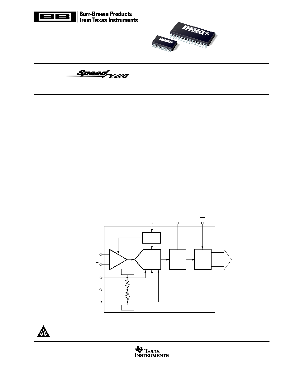
The ADS800 is a low power, monolithic 12-bit, 40MHz
Analog-to-Digital (A/D) converter utilizing a small geom-
etry CMOS process. This complete converter includes a
12-bit quantizer, wideband track/hold, reference and three-
state outputs. It operates from a single +5V power supply
and can be configured to accept either differential or single-
ended input signals.
The ADS800 employs digital error correction to provide
excellent Nyquist differential linearity performance for de-
manding imaging applications. Its low distortion, high SNR
and high oversampling capability give it the extra margin
needed for telecommunications, test instrumentation and
video applications.
This high performance A/D converter is specified over
temperature for AC and DC performance at a 40MHz
sampling rate. The ADS800 is available in SO-28 and
SSOP-28 packages.
Pipeline
A/D
Timing
Circuitry
Error
Correction
Logic
3-State
Outputs
T/H
12-Bit
Digital
Data
CLK
+1.25V
+3.25V
MSBI
OE
IN
IN
REFT
CM
REFB
TM
APPLICATIONS
q
IF AND BASEBAND DIGITIZATION
q
DIGITAL COMMUNICATIONS
q
ULTRASOUND IMAGING
q
GAMMA CAMERAS
q
TEST INSTRUMENTATION
q
CCD IMAGING
Copiers
Scanners
Cameras
q
VIDEO DIGITIZING
ADS800
SBAS035A APRIL 2001
www.ti.com
PRODUCTION DATA information is current as of publication date.
Products conform to specifications per the terms of Texas Instruments
standard warranty. Production processing does not necessarily include
testing of all parameters.
Copyright © 2001, Texas Instruments Incorporated
Please be aware that an important notice concerning availability, standard warranty, and use in critical applications of
Texas Instruments semiconductor products and disclaimers thereto appears at the end of this data sheet.
ADS800
2
SBAS035A
ADS800U (SOIC)
ADS800E (SSOP)
PARAMETER
CONDITIONS
TEMP
MIN
TYP
MAX
MIN
TYP
MAX
UNITS
ELECTRICAL CHARACTERISTICS
At T
A
= +25
°
C, V
S
= +5V, Sampling Rate = 40MHz, with a 50% duty cycle clock having a 2ns rise/fall time, unless otherwise noted.
TTL/HCT Compatible CMOS
Falling Edge
TTL/HCT Compatible CMOS
Falling Edge
ABSOLUTE MAXIMUM RATINGS
+V
S
....................................................................................................... +6V
Analog Input .............................................................. 0V to (+V
S
+ 300mV)
Logic Input ................................................................ 0V to (+V
S
+ 300mV)
Case Temperature ......................................................................... +100
°
C
Junction Temperature .................................................................... +150
°
C
Storage Temperature ..................................................................... +125
°
C
External Top Reference Voltage (REFT) .................................. +3.4V Max
External Bottom Reference Voltage (REFB) .............................. +1.1V Min
NOTE: (1) Stresses above these ratings may permanently damage the device.
ELECTROSTATIC
DISCHARGE SENSITIVITY
This integrated circuit can be damaged by ESD. Texas Instru-
ments recommends that all integrated circuits be handled with
appropriate precautions. Failure to observe proper handling
and installation procedures can cause damage.
ESD damage can range from subtle performance degradation
to complete device failure. Precision integrated circuits may
be more susceptible to damage because very small parametric
changes could cause the device not to meet its published
specifications.
PACKAGE
SPECIFIED
DRAWING
TEMPERATURE
PACKAGE
ORDERING
TRANSPORT
PRODUCT
PACKAGE
NUMBER
RANGE
MARKING
NUMBER
(1)
MEDIA
ADS800U
SO-28
217
40
°
C to +85
°
C
ADS800U
ADS800U
Rails
ADS800E
SSOP-28
324
40
°
C to +85
°
C
ADS800E
ADS800E
Rails
ADS800E
SSOP-28
324
40
°
C to +85
°
C
ADS800E
ADS800E/1K
Tape and Reel
PACKAGE/ORDERING INFORMATION
Resolution
12
Bits
Specified Temperature Range
T
AMBIENT
0
+70
(1)
°
C
Operating Temperature Range
T
AMBIENT
40
+85
°
C
ANALOG INPUT
Differential Full Scale Input Range
Both Inputs,
+1.25
+3.25
V
180
°
Out of Phase
Common-Mode Voltage
+2.25
V
Analog Input Bandwidth (3dB)
Small Signal
20dBFS
(2)
Input
+25
°
C
400
MHz
Full Power
0dBFS Input
+25
°
C
65
MHz
Input Impedance
1.25 || 4
M
|| pF
DIGITAL INPUT
Logic Family
Convert Command
Start Conversion
ACCURACY
(3)
f
S
= 2.5MHz
Gain Error
+25
°
C
±
0.4
±
1.5
%
Full
±
0.6
±
2.5
%
Gain Drift
±
95
ppm/
°
C
Power Supply Rejection of Gain
Delta +V
S
=
±
5%
+25
°
C
0.01
0.15
%FSR/%
Input Offset Error
Full
±
2.6
±
3.5
%
Power Supply Rejection of Offset
Delta +V
S
=
±
5%
+25
°
C
0.02
0.15
%FSR/%
CONVERSION CHARACTERISTICS
Sample Rate
10k
40M
Sample/s
Data Latency
6.5
Convert Cycle
DYNAMIC CHARACTERISTICS
Differential Linearity Error
f = 500kHz
t
H
= 13ns
(4)
+25
°
C
±
0.6
±
1.0
LSB
Full
±
0.8
LSB
f = 12MHz
+25
°
C
±
0.4
±
1.0
±
0.7
LSB
Full
±
0.5
±
0.8
LSB
No Missing Codes
t
H
= 13ns
(4)
+25
°
C
Guaranteed
Guaranteed
LSB
Integral Linearity Error at f = 500kHz
Full
±
1.9
LSB
Spurious-Free Dynamic Range (SFDR)
f = 500kHz (1dBFS input)
+25
°
C
65
72
dBFS
Full
60
66
dBFS
f = 12MHz (1dBFS input)
+25
°
C
58
61
dBFS
Full
55
61
dBFS
NOTE: (1) Models with a slash (/) are available only in Tape and Reel in the quantities indicated (e.g., /1K indicates 1000 devices per reel). Ordering 1000 pieces
of "ADS800/1K" will get a single 1000-piece Tape and Reel.
ADS800
3
SBAS035A
Two-Tone Intermodulation Distortion (IMD)
(5)
f = 4.4MHz and 4.5MHz (7dBFS each tone)
+25
°
C
63
dBc
Full
62
dBc
Signal-to-Noise Ratio (SNR)
f = 500kHz (1dBFS input)
+25
°
C
61
64
59
dB
Full
57
63
dB
f = 12MHz (1dBFS input)
+25
°
C
61
62
59
dB
Full
56
62
dB
Signal-to-(Noise + Distortion) (SINAD)
f = 500kHz (1dBFS input)
+25
°
C
59
63
57
dB
Full
54
64
dB
f = 12MHz (1dBFS input)
+25
°
C
56
58
54
dB
Full
51
57
dB
Differential Gain Error
NTSC or PAL
+25
°
C
0.5
%
Differential Phase Error
NTSC or PAL
+25
°
C
0.1
degrees
Aperture Delay Time
+25
°
C
2
ns
Aperture Jitter
+25
°
C
7
ps rms
Overvoltage Recovery Time
(6)
1.5x Full Scale Input
+25
°
C
2
ns
OUTPUTS
Logic Family
Logic Coding
Logic Selectable
Logic Levels
Logic "LO",
Full
0
0.4
V
C
L
= 15pF max
Logic "HI",
Full
+2.5
+V
S
V
C
L
= 15pF max
3-State Enable Time
20
40
ns
3-State Disable Time
Full
2
10
ns
POWER SUPPLY REQUIREMENTS
Supply Voltage: +V
S
Operating
Full
+4.75
+5.0
+5.25
V
Supply Current: +I
S
Operating
+25
°
C
78
93
mA
Operating
Full
78
97
mA
Power Consumption
Operating
+25
°
C
390
465
mW
Operating
Full
390
485
mW
Thermal Resistance,
JA
SO-28
75
°
C/W
SSOP-28
50
°
C/W
NOTE: (1) An asterisk (
) indicates same specifications as the ADS800U. (2) dBFS refers to dB below Full Scale. (3) Percentage accuracies are referred to the
internal A/D Full Scale Range of 4Vp-p. (4) Refer to Timing Diagram footnotes for the guaranteed differential linearity performance and no missing codes condition
for the SOIC and SSOP packages. (5) IMD is referred to the larger of the two input signals. If referred to the peak envelope signal (
0dB), the intermodulation
products will be 7dB lower. (6) No "rollover" of bits.
ADS800U (SOIC)
ADS800E (SSOP)
PARAMETER
CONDITIONS
TEMP
MIN
TYP
MAX
MIN
TYP
MAX
UNITS
TTL/HCT Compatible CMOS
SOB or BTC
TTL/HCT Compatible CMOS
SOB or BTC
ELECTRICAL CHARACTERISTICS
(Cont.)
At T
A
= +25
°
C, V
S
= +5V, Sampling Rate = 40MHz, with a 50% duty cycle clock having a 2ns rise/fall time, unless otherwise noted.
ADS800
4
SBAS035A
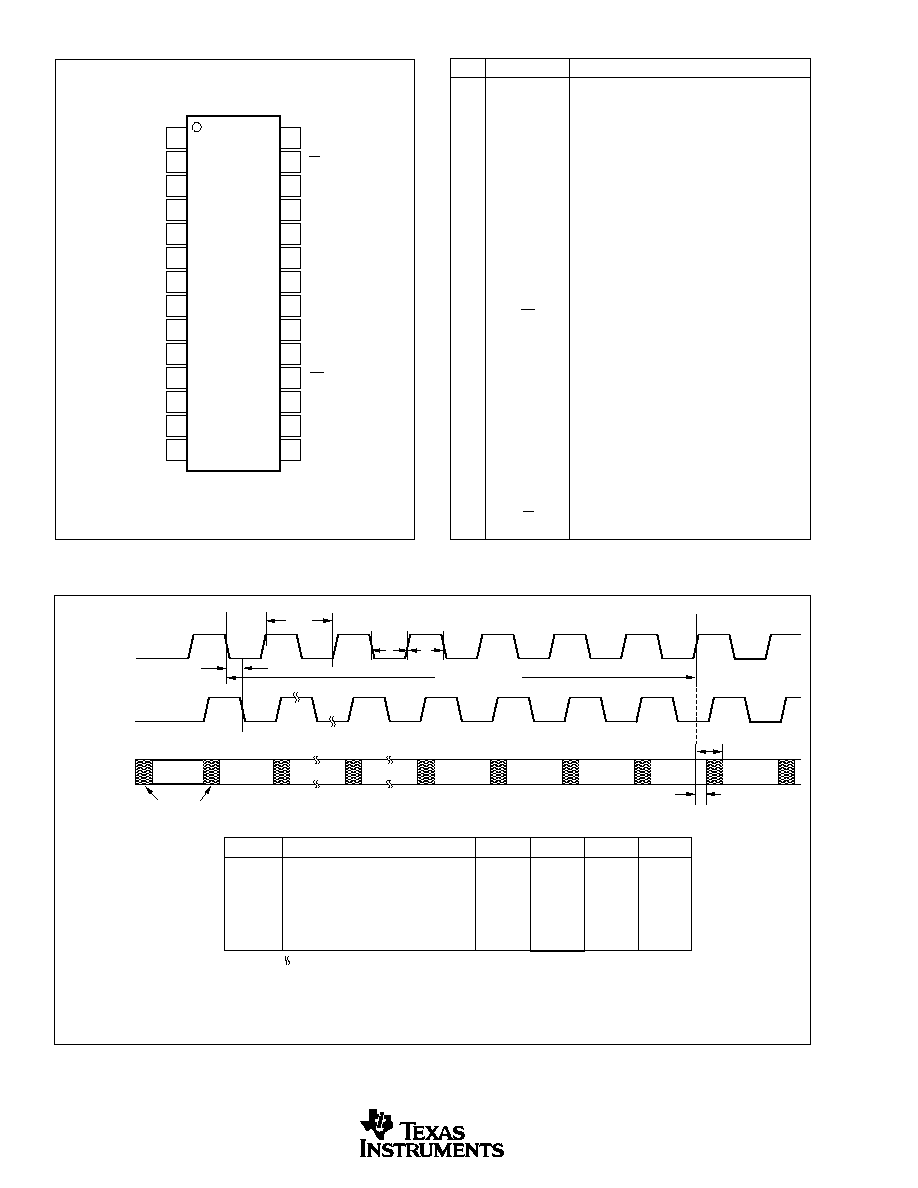
PIN CONFIGURATION
TOP VIEW
SOIC/SSOP
PIN
DESIGNATOR
DESCRIPTION
1
GND
Ground
2
B1
Bit 1, Most Significant Bit
3
B2
Bit 2
4
B3
Bit 3
5
B4
Bit 4
6
B5
Bit 5
7
B6
Bit 6
8
B7
Bit 7
9
B8
Bit 8
10
B9
Bit 9
11
B10
Bit 10
12
B11
Bit 11
13
B12
Bit 12, Least Significant Bit
14
GND
Ground
15
+V
S
+5V Power Supply
16
CLK
Convert Clock Input, 50% Duty Cycle
17
+V
S
+5V Power Supply
18
OE
HI: High Impedance State. LO or Floating: Nor-
mal Operation. Internal pull-down resistors.
19
MSBI
Most Significant Bit Inversion, HI: MSB inverted
for complementary output. LO or Floating: Straight
output. Internal pull-down resistors.
20
+V
S
+5V Power Supply
21
REFB
Bottom Reference Bypass. For external bypass-
ing of internal +1.25V reference.
22
CM
Common-Mode Voltage. It is derived by (REFT +
REFB)/2.
23
REFT
Top Reference Bypass. For external bypassing
of internal +3.25V reference.
24
+V
S
+5V Power Supply
25
GND
Ground
26
IN
Input
27
IN
Complementary Input
28
GND
Ground
PIN DESCRIPTIONS
GND
B1
B2
B3
B4
B5
B6
B7
B8
B9
B10
B11
B12
GND
GND
IN
IN
GND
+V
S
REFT
CM
REFB
+V
S
MSBI
OE
+V
S
CLK
+V
S
1
2
3
4
5
6
7
8
9
10
11
12
13
14
28
27
26
25
24
23
22
21
20
19
18
17
16
15
ADS800
TIMING DIAGRAM
SYMBOL
DESCRIPTION
MIN
TYP
MAX
UNITS
t
CONV
Convert Clock Period
25
100
µ
s
ns
t
L
Clock Pulse Low
12
12.5
ns
t
H
Clock Pulse High
12
(2)
12.5
ns
t
D
Aperture Delay
2
ns
t
1
Data Hold Time, C
L
= 0pF
3.9
ns
t
2
New Data Delay Time, C
L
= 15pF max
12.5
ns
NOTE: (1) " " indicates the portion of the waveform that will stretch out at slower sample rates.
(2) t
H
must be 13ns minimum if no missing codes is desired only for the conditions of t
CONV
28ns
and f
IN
<2MHz for the SOIC package. For best performance in the SSOP package, t
H
must be 13ns
minimum for all input frequencies and t
CONV
28ns. Refer to the Clock Requirements for a possible
clock skew circuit for this condition.
Track
Hold
"N"
Hold
"N + 1"
Hold
"N + 2"
Hold
"N + 3"
Hold
"N + 4"
Hold
"N + 5"
Hold
"N + 6"
Track
Data Valid
N-7
Data Valid
N-6
INTERNAL
TRACK/HOLD
CONVERT
CLOCK
OUTPUT
DATA
t
D
t
2
t
1
DATA LATENCY
(6.5 Clock Cycles)
t
CONV
t
L
t
H
Track
Track
Track
Track
N-3
N-5
N-4
N-2
N-1
N
Track
Track
Data Valid
N-8
(1)
Data Invalid
ADS800
5
SBAS035A
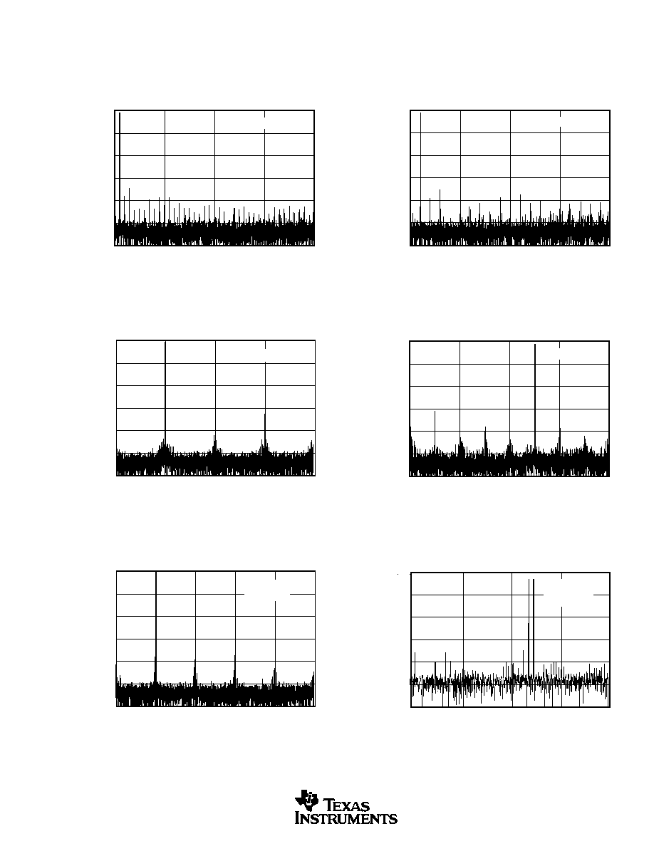
SPECTRAL PERFORMANCE
Frequency (MHz)
Amplitude (dB)
0
5
10
15
20
0
20
40
60
80
100
120
f
IN
= 12MHz
SPECTRAL PERFORMANCE
Frequency (MHz)
Amplitude (dB)
0
5
10
15
20
0
20
40
60
80
100
120
f
IN
= 500kHz
TYPICAL CHARACTERISTICS
At T
A
= +25
°
C, V
S
= +5V, Sampling Rate = 40MHz, with a 50% duty cycle clock having a 2ns rise/fall time, unless otherwise noted.
SPECTRAL PERFORMANCE
Frequency (MHz)
Amplitude (dB)
0
5
10
15
20
0
20
40
60
80
100
120
f
IN
= 1MHz
0
20
40
60
80
100
120
SPECTRAL PERFORMANCE
Frequency (MHz)
Amplitude (dB)
0
5
10
15
20
f
IN
= 5MHz
0
20
40
60
80
100
120
SPECTRAL PERFORMANCE
Frequency (MHz)
Amplitude (dB)
0
1.0
2.0
3.0
4.0
5.0
f
IN
= 1MHz
f
S
= 10MHz
0
20
40
60
80
100
120
TWO-TONE INTERMODULATION
Amplitude (dB)
0.0
5.0
10.0
15.0
20.0
Frequency (MHz)
f
1
= 12.5MHz
f
2
= 12.0MHz