 | –≠–ª–µ–∫—Ç—Ä–æ–Ω–Ω—ã–π –∫–æ–º–ø–æ–Ω–µ–Ω—Ç: ADS803 | –°–∫–∞—á–∞—Ç—å:  PDF PDF  ZIP ZIP |
Document Outline
- FEATURES
- APPLICATIONS
- DESCRIPTION
- ABSOLUTE MAXIMUM RATINGS
- PACKAGE/ORDERING INFORMATION
- ELECTRICAL CHARACTERISTICS
- DEVICE INFORMATION
- PIN CONFIGURATION
- PIN DESCRIPTIONS
- TIMING DIAGRAM
- TYPICAL CHARACTERISTICS
- APPLICATION INFORMATION
- DRIVING THE ANALOG INPUT
- AC-COUPLED INPUT CONFIGURATION
- DC-COUPLED WITHOUT LEVEL SHIFT
- DC-COUPLED WITH LEVEL SHIFT
- SINGLE-ENDED-TO-DIFFERENTIAL CONFIGURATION (TRANSFORMER COUPLED)
- REFERENCE OPERATION
- SELECTING THE INPUT RANGE AND REFERENCE
- EXTERNAL REFERENCE OPERATION
- DIGITAL INPUTS AND OUTPUTS
- CLOCK INPUT REQUIREMENTS
- DIGITAL OUTPUTS
- GROUNDING AND DECOUPLING
- PACKAGE DRAWING
- DB (R-PDSO-G**) PLASTIC SMALL-OUTLINE
12-Bit, 5MHz Sampling
ANALOG-TO-DIGITAL CONVERTER
FEATURES
q
HIGH SFDR: 82dB at NYQUIST
q
HIGH SNR: 69dB
q
LOW POWER: 115mW
q
LOW DLE: 0.25LSB
q
FLEXIBLE INPUT RANGE
q
OVER-RANGE INDICATOR
APPLICATIONS
q
IF AND BASEBAND DIGITIZATION
q
CCD IMAGING SCANNERS
q
TEST INSTRUMENTATION
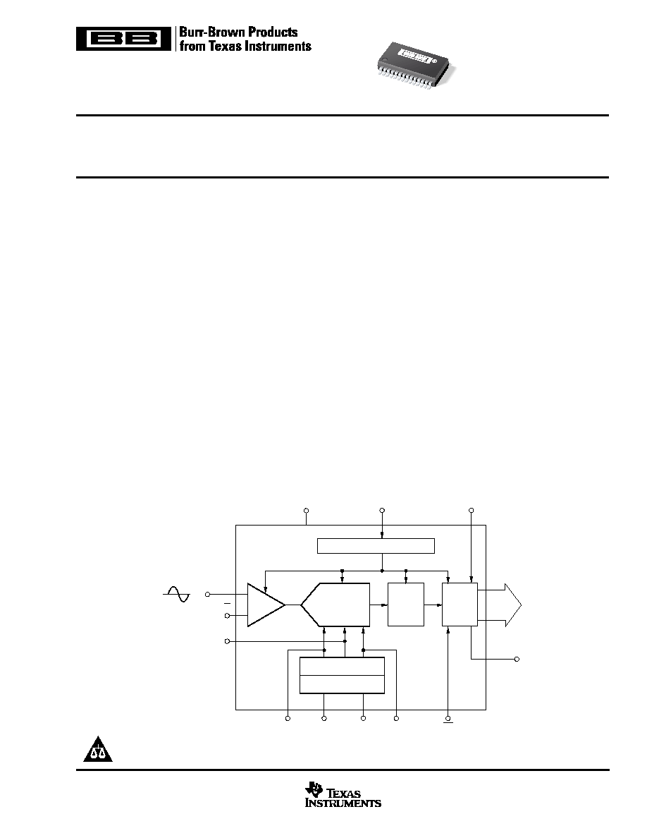
DESCRIPTION
The ADS803 is a high-speed, high dynamic range, 12-bit
pipelined Analog-to-Digital (A/D) converter. This converter
includes a high-bandwidth track-and-hold that gives excel-
lent spurious performance up to and beyond the Nyquist rate.
This high-bandwidth, linear track-and-hold minimizes har-
monics and has low jitter, leading to excellent SNR perfor-
mance. The ADS803 is also pin-compatible with the 10MHz
ADS804 and the 20MHz ADS805.
The ADS803 provides an internal reference and can be
programmed for a 2Vp-p input range for the best spurious
performance and ease of driving. Alternatively, the 5Vp-p input
range can be used for the lowest input referred noise of
0.09LSBs rms giving superior imaging performance. There is
also a capability to set the input range in between the 2Vp-p
and 5Vp-p input ranges or to use an external reference. The
ADS803 also provides an over-range indicator flag to indicate
an input range that exceeds the full-scale input range of the
converter. This flag can be used to reduce the gain of the front-
end gain-ranging circuitry.
The ADS803 employs digital error-correction techniques to
provide excellent differential linearity for demanding imaging
applications. Its low distortion and high SNR give the extra
margin needed for communications, medical imaging, video,
and test instrumentation applications. The ADS803 is avail-
able in an SSOP-28 package.
12-Bit
Pipelined
ADC
Reference and
Mode Select
Reference Ladder
and Driver
Timing Circuitry
Error
Correction
Logic
3-State
Outputs
T & H
D0
D11
∑
∑
∑
CLK
+V
S
ADS803
VDRV
OE
SEL
REFB
V
REF
REFT
IN
V
IN
IN
CM
OVR
ADS803
SBAS074B ≠ JANUARY 1997 ≠ REVISED SEPTEMBER 2002
www.ti.com
Copyright © 1997, Texas Instruments Incorporated
Please be aware that an important notice concerning availability, standard warranty, and use in critical applications of
Texas Instruments semiconductor products and disclaimers thereto appears at the end of this data sheet.
PRODUCTION DATA information is current as of publication date.
Products conform to specifications per the terms of Texas Instruments
standard warranty. Production processing does not necessarily include
testing of all parameters.
ADS8
03E

ADS803
2
SBAS074B
www.ti.com
+V
S
....................................................................................................... +6V
Analog Input ........................................................... (≠0.3V) to (+V
S
+0.3V)
Logic Input ............................................................. (≠0.3V) to (+V
S
+0.3V)
Case Temperature ......................................................................... +100
∞
C
Junction Temperature .................................................................... +150
∞
C
Storage Temperature ..................................................................... +150
∞
C
ABSOLUTE MAXIMUM RATINGS
(1)
ELECTRICAL CHARACTERISTICS
At T
A
= full specified temperature range, V
S
= +5V, specified input range = 1.5V to 3.5V, single-ended input and sampling rate = 5MHz, unless otherwise specified.
ADS803E
PARAMETER
CONDITIONS
MIN
TYP
MAX
UNITS
RESOLUTION
12 Tested
Bits
SPECIFIED TEMPERATURE RANGE
≠40
+85
∞
C
CONVERSION CHARACTERISTICS
Sample Rate
10k
5M
Samples/s
Data Latency
6
Clk Cycles
ANALOG INPUT
Single-Ended Input Range
1.5
3.5
V
Standard Optional Single-Ended Input Range
0
5
V
Common-Mode Voltage
2.5
V
Standard Optional Common-Mode Voltage
1
V
Input Capacitance
20
pF
Track-Mode Input Bandwidth
≠3dBFS Input
270
MHz
DYNAMIC CHARACTERISTICS
Differential Linearity Error (Largest Code Error)
f = 500kHz
±
0.25
±
0.75
LSB
No Missing Codes
Tested
Spurious-Free Dynamic Range
(1)
f = 2.48MHz (≠1dB input)
74
82
dBFS
(2)
2-Tone Intermodulation Distortion
(3)
74
dBc
f = 1.8M and 1.9M (≠7dBFS each tone)
Signal-to-Noise Ratio (SNR)
f = 2.48MHz (≠1dB input)
66.5
69
dB
Signal-to-(Noise + Distortion) (SINAD)
f = 2.48MHz (≠1dB input)
65
68
dB
Effective Number of Bits at 2.48MHz
(4)
11
Bits
Input Referred Noise
0V to 5V Input
0.09
LSBs rms
1.5V to 3.5V Input
0.23
LSBs rms
Integral Nonlinearity Error
f = 500kHz
±
1
±
2
LSB
Aperture Delay Time
1
ns
Aperture Jitter
4
ps rms
Over-Voltage Recovery Time
1.5 ∑ FS Input
2
ns
Full-Scale Step Acquisition Time
50
ns
SPECIFIED
PACKAGE
TEMPERATURE
PACKAGE
ORDERING
TRANSPORT
PRODUCT
PACKAGE-LEAD
DESIGNATOR
(1)
RANGE
MARKING
NUMBER
MEDIA, QUANTITY
ADS803E
SSOP-28
DB
≠40
∞
C to +85
∞
C
ADS803E
ADS803E
Rails, 48
"
"
"
"
"
ADS803E/1K
Tape and Reel, 1000
NOTE: (1) For the most current specifications and package information, refer to our web site at www.ti.com.
PACKAGE/ORDERING INFORMATION
ELECTROSTATIC
DISCHARGE SENSITIVITY
This integrated circuit can be damaged by ESD. Texas Instru-
ments recommends that all integrated circuits be handled with
appropriate precautions. Failure to observe proper handling
and installation procedures can cause damage.
ESD damage can range from subtle performance degrada-
tion to complete device failure. Precision integrated circuits
may be more susceptible to damage because very small
parametric changes could cause the device not to meet its
published specifications.
NOTE: (1) Stresses above those listed under "Absolute Maximum Ratings"
may cause permanent damage to the device. Exposure to absolute maximum
conditions for extended periods may affect device reliability.
ADS803
3
SBAS074B
www.ti.com
ELECTRICAL CHARACTERISTICS
(Cont.)
At T
A
= full specified temperature range, V
S
= +5V, specified input range = 1.5V to 3.5V, single-ended input and sampling rate = 5MHz, unless otherwise specified.
ADS803E
PARAMETER
CONDITIONS
MIN
TYP
MAX
UNITS
DIGITAL INPUTS
Logic Family
CMOS Compatible
Convert Command
Start Conversion
Rising Edge of Convert Clock
High Level Input Current (V
IN
= 5V)
(5)
100
µ
A
Low Level Input Current (V
IN
= 0V)
±
10
µ
A
High Level Input Voltage
+3.5
V
Low Level Input Voltage
+1.0
V
Input Capacitance
5
pF
DIGITAL OUTPUTS
Logic Family
CMOS/TTL Compatible
V
Logic Coding
Straight Offset Binary
Low Output Voltage
(I
OL
= 50
µ
A)
0.1
V
Low Output Voltage
(I
OL
= 1.6mA)
0.4
V
High Output Voltage
(I
OH
= 50
µ
A)
+4.5
V
High Output Voltage
(I
OH
= 0.5mA)
+2.4
V
3-State Enable Time
OE = L
20
40
ns
3-State Disable Time
OE = H
2
10
ns
Output Capacitance
5
pF
ACCURACY (5Vp-p Input Range)
f
S
= 2.5MHz
Zero Error (Referred to ≠FS)
At 25
∞
C
0.2
±
1.5
%FS
Zero Error Drift (Referred to ≠FS)
±
5
ppm/
∞
C
Gain Error
(6)
At 25
∞
C
±
2.0
%FS
Gain Error Drift
(6)
±
15
ppm/
∞
C
Gain Error
(7)
At 25
∞
C
±
1.5
%FS
Gain Error Drift
(7)
±
15
ppm/
∞
C
Power-Supply Rejection of Gain
V
S
=
±
5%
60
82
dB
Reference Input Resistance
1.6
k
Internal Voltage Reference Tolerance (V
REF
= 2.5V)
At 25
∞
C
±
35
mV
Internal Voltage Reference Tolerance (V
REF
= 1.0V)
At 25
∞
C
±
14
mV
POWER-SUPPLY REQUIREMENTS
Supply Voltage: +V
S
Operating
+4.7
+5.0
5.3
V
Supply Current: +I
S
Operating
23
27
mA
Power Dissipation
Operating
115
135
mW
Thermal Resistance,
JA
SSOP-28
50
∞
C/W
NOTES: (1) Spurious-Free Dynamic Range refers to the magnitude of the largest harmonic. (2) dBFS means dB relative to full-scale. (3) 2-tone intermodulation
distortion is referred to the largest fundamental tone. This number will be 6dB higher if it is referred to the magnitude of the 2-tone fundamental envelope. (4) Effective
number of bits (ENOB) is defined by (SINAD ≠ 1.76)/6.02. (5) Internal 50k
pull-down resistor. (6) Includes internal reference. (7) Excludes internal reference.
ADS803
4
SBAS074B
www.ti.com
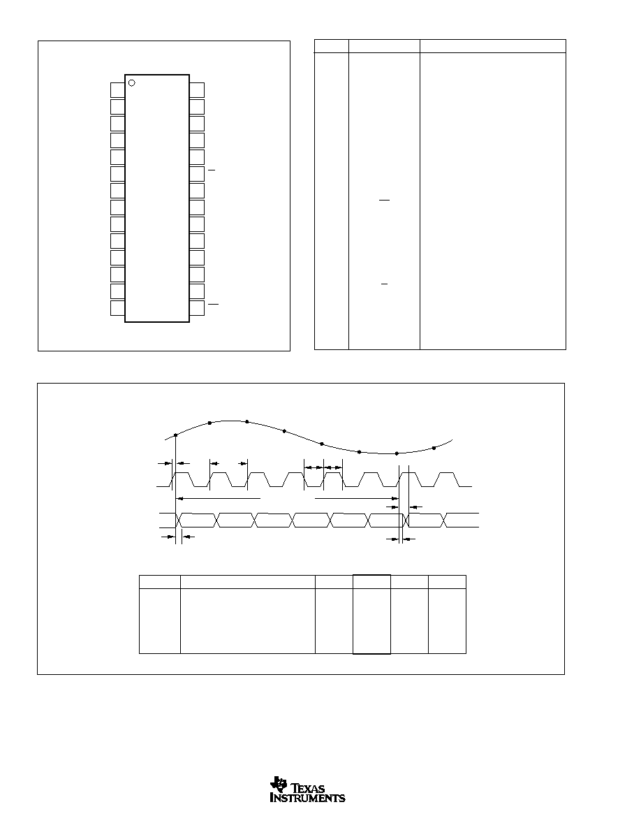
PIN CONFIGURATION
PIN
DESIGNATOR
DESCRIPTION
1
OVR
Over-Range Indicator
2
B1
Data Bit 1 (MSB)
3
B2
Data Bit 2
4
B3
Data Bit 3
5
B4
Data Bit 4
6
B5
Data Bit 5
7
B6
Data Bit 6
8
B7
Data Bit 7
9
B8
Data Bit 8
10
B9
Data Bit 9
11
B10
Data Bit 10
12
B11
Data Bit 11
13
B12
Data Bit 12 (LSB)
14
CLK
Convert Clock Input
15
OE
Output Enable
16
+V
S
+5V Supply
17
GND
Ground
18
SEL
Input Range Select
19
V
REF
Reference Voltage Select
20
REFB
Bottom Reference
21
CM
Common-Mode Voltage
22
REFT
Top Reference
23
IN
Complementary Analog Input
24
GND
Analog Ground
25
IN
Analog Input (+)
26
GND
Analog Ground
27
+V
S
+5V Supply
28
VDRV
Output Driver Voltage
PIN DESCRIPTIONS
Top View
SSOP
6 Clock Cycles
Data Invalid
t
D
t
L
t
H
t
CONV
N ≠ 6
N ≠ 5
N ≠ 4
N ≠ 3
N ≠ 2
N ≠ 1
N
N + 1
Data Out
Clock
Analog In
N
t
2
N + 1
N + 2
N + 3
N + 4
N + 5
N + 6
N + 7
t
1
TIMING DIAGRAM
SYMBOL
DESCRIPTION
MIN
TYP
MAX
UNITS
t
CONV
Convert Clock Period
200
1 ∑ 10
5
(ns)
ns
t
L
Clock Pulse LOW
96
99
ns
t
H
Clock Pulse HIGH
96
99
ns
t
D
Aperture Delay
3
ns
t
1
Data Hold Time, C
L
= 0pF
3.9
ns
t
2
New Data Delay Time, C
L
= 15pF max
12
ns
OVR
B1
B2
B3
B4
B5
B6
B7
B8
B9
B10
B11
B12
CLK
VDRV
+V
S
GND
IN
GND
IN
REFT
CM
REFB
VREF
SEL
GND
+V
S
OE
1
2
3
4
5
6
7
8
9
10
11
12
13
14
28
27
26
25
24
23
22
21
20
19
18
17
16
15
ADS803

ADS803
5
SBAS074B
www.ti.com
TYPICAL CHARACTERISTICS
At T
A
= full specified temperature range, V
S
= +5V, specified input range = 1.5V to 3.5V, and single-ended input and sampling rate = 5MHz, unless otherwise specified.
SPECTRAL PERFORMANCE
Frequency (MHz)
Amplitude (dB)
0
0.5
1.0
1.5
2.0
2.5
0
≠20
≠40
≠60
≠80
≠100
≠120
f
IN
= 500kHz
SPECTRAL PERFORMANCE
Frequency (MHz)
Amplitude (dB)
0
0.5
1.0
1.5
2.0
2.5
0
≠20
≠40
≠60
≠80
≠100
≠120
f
IN
= 2.48MHz
FREQUENCY SPECTRUM
Frequency (MHz)
Magnitude (dBFSR)
0
0.5
1.0
1.5
2.0
2.5
0
≠20
≠40
≠60
≠80
≠100
≠120
f
1
= 1.8MHz at ≠7dB
f
2
= 1.9MHz at ≠7dB
IMD (3) = ≠74dBc
DIFFERENTIAL LINEARITY ERROR
Output Code
DLE (LSB)
0
1024
2048
3072
4096
1.0
0.5
0
≠0.5
≠1.0
f
IN
= 500kHz
INTEGRAL LINEARITY ERROR
Output Code
ILE (LSB)
0
1024
2048
3072
4096
4.0
2.0
0
≠2.0
≠4.0
f
IN
= 500kHz
100
80
60
40
20
0
SWEPT POWER SFDR
SFDR (dBFS, dBc)
≠60
≠50
≠40
≠30
≠20
≠10
0
Input Amplitude (dBFS)
dBFS
dBc
f
IN
= 2.48MHz