 | ÐлекÑÑоннÑй компоненÑ: AIC111 | СкаÑаÑÑ:  PDF PDF  ZIP ZIP |
Äîêóìåíòàöèÿ è îïèñàíèÿ www.docs.chipfind.ru
AIC111
SLAS382 JUNE 2003
IC DESIGN SPECIFICATION
1.3-V microPower
DSP/
µ
C VOICE BAND AUDIO CODEC
FEATURES
D
Single Channel Codec
D
Noise Shaped Delta Sigma ADC and DAC
Technology
D
Low Supply Voltage and Current:
1.3-V Typical Power Supply
350-
µ
A Typical Supply Current Drain
D
Power Supply Up Monitor and Low Battery
Monitor That Also Automatically Shuts Off
H-Bridge Output When Battery Decays Below
1.05 V in a Nontransient Manner
D
Typical 2.4-
µ
Vrms Input Referred Noise With
0.01% Total Harmonic Distortion for Front
End and 108-dB Dynamic Range
D
ADC Has 87-dB Dynamic Range With 73-dB
Total Harmonic Distortion 100 Hz10 kHz,
40-kHz Sampling Rate
D
Typical 55-dB PSRR 100 Hz to 10 kHz for
Analog Front End
D
Low Noise Programmable Gain
Amplifier/Compressor Front End With
Programmable Fast and Slow Attack and
Decay Rates With Dual or Single Attack and
Decay Rate Option
D
Typical Output Noise of 12
µ
Vrms With 0.05%
Total Harmonic Distortion for Delta Sigma
DAC and H-Bridge Output Driver
D
Low Jitter Oscillator That Generates all
Internal Clocks and Generates 5-MHz Output
DSP/
µ
C Clock
D
Regulated Bandgap Voltage Reference
D
Programmable Functionality via Digital Serial
Interface
McBSP Interface, DSP Protocol
TI TMS320VC54x
, TMS320VC55x
DSPs
SPI Interface, Microcontroller Protocol
TI MSP430xx
D
External Chip Power Down and Reset
D
Available in:
32-Pin QFN 5
×
5-mm Plastic Package
32-Pad Bumped Die in Waffle Pack (wafer
scale packaging), or Tape and Reel,
(Preview, Available 3rd Quarter 2003)
APPLICATIONS
D
Hearing Instruments
D
Personal Medical Devices
D
Hearing Protection
D
Aural Processing
D
Low-Power Headsets
DESCRIPTION
The AIC111 IC design specification serves to provide
product development teams with a guideline for how the
AIC111 IC is specified and programmable options that are
available. The document outlines a top-level block
description of the IC along with system specifications and
functions. Individual block descriptions and target
specifications are also outlined.
The Texas Instruments AIC111 is a TI
µ
Power DSP
compatible, or microcontroller compatible audio codec
product, or analog interface circuit. The AIC111 is part of
a comprehensive family of DSP/
µ
C based high-
performance analog interface solutions. The AIC111 is
targeted primarily at personal medical devices, such as
hearing instruments, aural preprocessing applications,
and low-power headset applications. The AIC111 is used
in any design requiring a programmable time constant
PGA/compressor interface,
high
dynamic
range
analog-to-digital converter, an external DSP/
µ
C
handling signal processing, or a low distortion
digital-to-analog converter with a balanced H-Bridge
speaker driver. It supports a CMOS digital interface
tailored for TI DSPs with the McBSP protocol such as
TMS320VC54x
DSP family and SPI-based controllers
such as TI MSP430x family of microcontrollers. The
AIC111 also has an external microphone or sensor supply
and bias and power supply up low-battery monitor
indicator.
This document contains information on products in more than one phase of
development. The status of each device is indicated on the page(s) specifying its
electrical characteristics.
Please be aware that an important notice concerning availability, standard warranty, and use in critical applications of Texas Instruments
semiconductor products and disclaimers thereto appears at the end of this data sheet.
www.ti.com
Copyright
2003, Texas Instruments Incorporated
AIC111
SLAS382 JUNE 2003
www.ti.com
2
These devices have limited built-in ESD protection. The leads should be shorted together or the device placed in conductive foam during
storage or handling to prevent electrostatic damage to the MOS gates.
The AIC111 comes in a 32-pin QFN 5
×
5-mm package. A 32-pad solder ball bumped flip chip die that comes in waffle
packs or tape and reel is in preview and will be available 3rd quarter 2003.
AVAILABLE OPTIONS
PART NUMBER
PACKAGE
AIC111RHB
32-pin QFN (5 mm x 5 mm), in tube.
AIC111RHBR
32-pin QFN (5 mm x 5 mm), tape and reel
AIC111YE
32-pad waffle scale chip package, bumped die in waffle pack (contact the factory for availability) Preview,
available 3rd quarter 2003
AIC111YER
32-pad (WSCP) bumped die in tape and reel (contact the factory for availability) Preview, available 3rd
quarter 2003
ABSOLUTE MAXIMUM RATINGS
over operating free-air temperature range unless otherwise noted(1)(2)
UNIT
Input voltage
AI or DI pins
0.3 V to 4 V
Power supply
VDD, power pins
0.3 V to 4.5 V
Latch-up tolerance
JEDEC latch-up (EIA/JEDS78)
100 mA
Operating free-air temperature range, TA
0
°
C to 70
°
C
Functional temperature range
15
°
C to 85
°
C
Reflow temperature range (flip chip)
220
°
C to 230
°
C
Storage temperature range, Tstg
40
°
C to 125
°
C
Storage humidity
65% R.H.
(1) Stresses beyond those listed under absolute maximum ratings may cause permanent damage to the device. These are stress ratings only, and
functional operation of the device at these or any other conditions beyond those indicated under recommended operating conditions is not implied.
Exposure to absolute-maximum-rated conditions for extended periods may affect device reliability.
(2) Specifications are assured operating at maximum device limits for QFN package only, unless otherwise specified.
ELECTRICAL CHARACTERISTICS
INPUT/OUTPUT, OPERATING TEMPERATURE AT 25
°
C
PARAMETER
TEST CONDITION
MIN
TYP
MAX
UNIT
Digital interface (see Notes 1 and 2)
BUF_DVDD (see Note 1)
3.6
V
VIH High-level input voltage
BUF_DVDD0.2
V
VIL Low-level input voltage
BUF_DVSS+0.2
V
VOH High-level output voltage
BUF_DVDD
V
VOL Low-level output voltage
BUF_DVSS
V
Maximum allowed input voltage (AVIN)
Differential
450
mVpk
Input impedance (AVIN) (see Note 3)
Nominal gain = 50x
20
k
Input capacitance (AVIN)
5
pF
Microphone bias voltage (MIC_VSUP)
20-
µ
A maximum
0.87
0.94
0.99
V
Microphone bias resistor (MIC_BIAS)
27
29.1
31
k
H bridge amplifier output
DAC full scale output differential
Fixed Q
3/4 HB_VDD
V
H-bridge amplifier output
DAC full scale output differential
Adaptive Q
HB_VDD
VPP
Output resistance
Differential, HB VDD = 1.3 V
20 or 40
(1) DVDD, VDD_OSC, and AVDD should be within 50 mV, preferably connected together.
AVSS1, 2, DVSS, and VSS_OSC should be within 50 mV, preferably connected together.
(2) Maximum (0.9 V, DVDD 0.5 V)
BUF_DVDD
3.6 V
(3) Driving single-ended: Rin = R
×
[(1+A)/(2+A)], A = PGAC Gain (linear), R = 20.4 k
for A
4 or 20.4 k
×
(4/A) for A<4.
Rin(min) = 17 k
(A=4), Rin(max) = 59.89 k
(A = 0.89), Rin(nom) = 20 k
(A = 50).
AIC111
SLAS382 JUNE 2003
www.ti.com
3
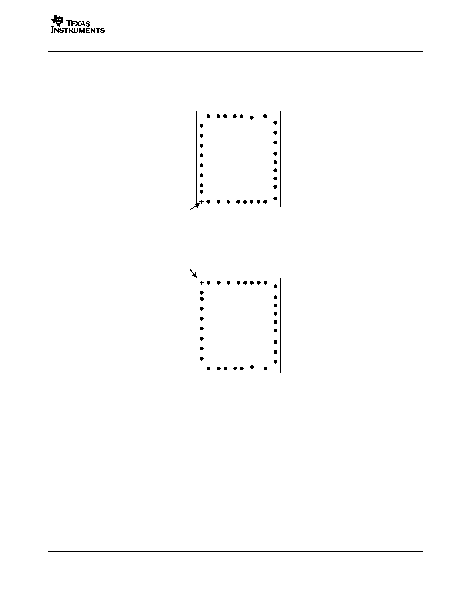
TERMINAL ASSIGNMENTS
Bumped Side
Bumped View
SUB_VSS
AIC111
HB_VDD
4
1
2
3
5
6
7
8
VMID_FILT
AVSS1
AVSS2
VREF
AVINM
AVINP
MIC_BIAS
MIC_VSUP
16
VDD_OSC
VOUT_P
17
18
19
HB_VSS_P
VOUT_M
HB_VSS_M
22
20
21
SCLK
FRAME
VRFIL
T
A
V
SS_REF
A
VDD
28
27
26
25
24
29
30
23
9
10
11
12 13 14
EXT_RST/PWDN
DVSS1
15
DVDD
VSS_OSC
IMODE
MCLK
BUF_DVDD
BUF_DVSS
SDOUT
SDIN
31
32
RST/LBM
Back Side
PCB View
For exact bump
location see Spec.
Section 2.2
SUB_VSS
AIC111
HB_VDD
4
1
2
3
5
6
7
8
VMID_FILT
AVSS1
AVSS2
VREF
AVINM
AVINP
MIC_BIAS
MIC_VSUP
16
VDD_OSC
VOUT_P
17
18
19
HB_VSS_P
VOUT_M
HB_VSS_M
22
20
21
SCLK
DVSS2
FRAME
VRFIL
T
A
VSS_REF
A
VDD
28
27
26
25
24
29
30
23
9
10
11
12 13 14
EXT_RST/PWDN
DVSS1
15
DVDD
VSS_OSC
IMODE
MCLK
BUF_DVDD
BUF_DVSS
SDOUT
SDIN
31
32
RST/LBM
Alignment
Marker
(0,0)
DVSS2
Figure 1. AIC111YE Bumped View and PCB Flipped Pin Placements

AIC111
SLAS382 JUNE 2003
www.ti.com
4
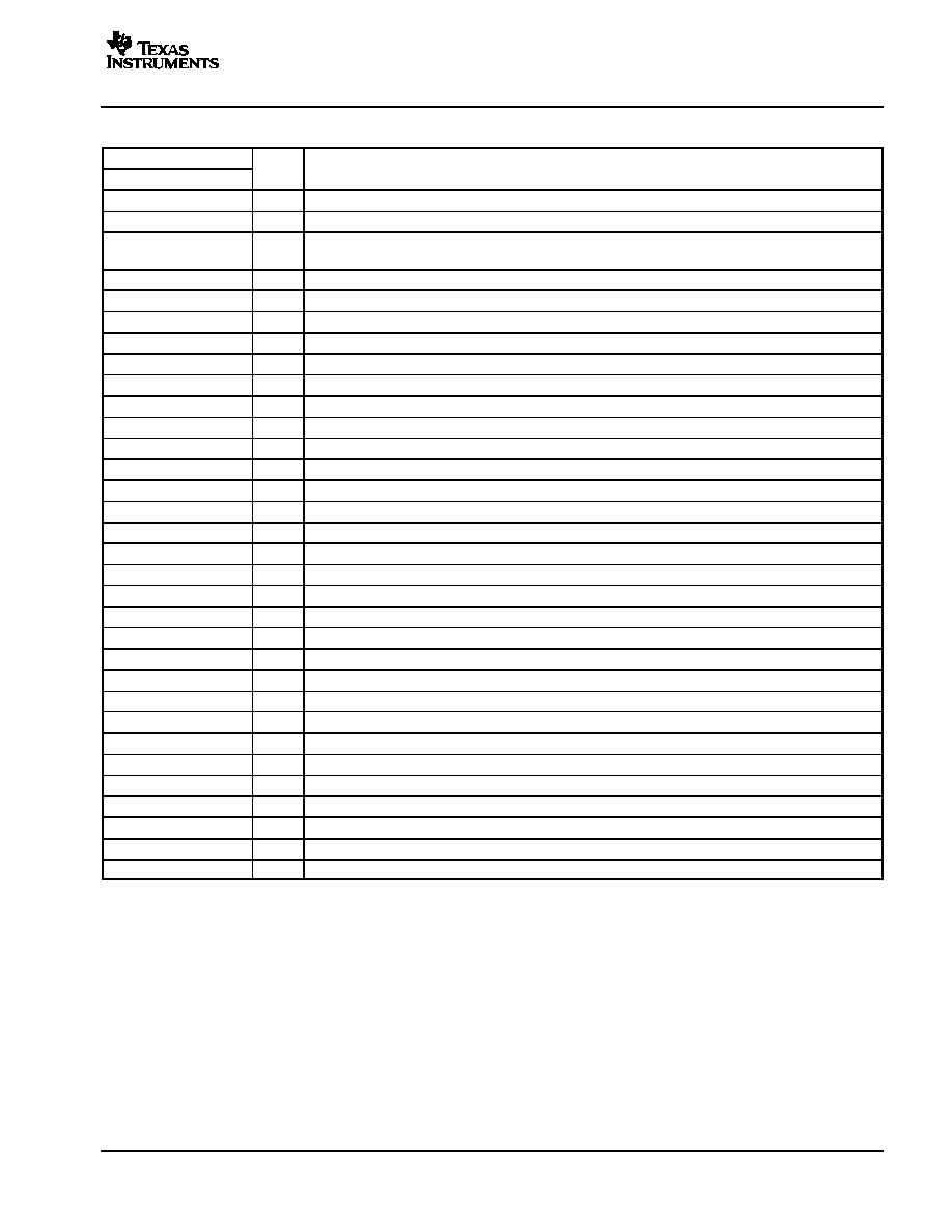
1
2
3
4
5
6
7
8
9
10
11
12
13
14
15
16
17
18
19
20
21
22
23
24
25
26
27
28
29
30
31
32
VDD_OSC
VSS_OSC
SUB_VSS
MCLK
DVDD
MIC_VSUP
AVSS1
AVINM
AVINP
AVSS2
VRFIL
T
A
VSS_REF
VREF_BG
A
VDD
DVSS
DVSS
VMID_FILT
MIC_BIAS
IMODE
SDOUT
FRAME
SDIN
SCLK
BUF_DVDD
RST/LBM
HB_VSS_M
VOUT_M
HB_VDD
VOUT_P
HB_VSS_P
BUF_DVSS
DVSS
AIC111RHB
Figure 2. AIC111RHB 32-Pin QFN Pinout
AIC111
SLAS382 JUNE 2003
www.ti.com
5
Terminal Functions
TERMINAL
TYPE
DESCRIPTION
NO.
NAME
TYPE
DESCRIPTION
1
AVSS1
GND
Ground return for ADC analog circuits
2
AVSS2
GND
Ground return for PGAC and MIC power analog circuits
3
AVINP
AI
Noninverting differential analog input coupled through an external 1-
µ
F capacitor to external microphone
output
4
AVINM
AI
Inverting differential analog signal input coupled through an external 1-
µ
F capacitor to ground
5
VMID_FILT
AO
Midsupply ac ground reference filter pin bypassed by a 1-
µ
F capacitor connected to ground
6
MIC_BIAS
AO
Source connection of external microphone source follower preamp. (Provides 29.1 k
to AVSS2
)
7
VREF
AO
Bandgap reference output bypassed by external 1-
µ
F VREF filter capacitor
8
MIC_VSUP
AO
Supply voltage for external microphone source follower preamp bypassed with an external 0.1-
µ
F capacitor
9
SUB_VSS
GND
Isolated substrate VSS for analog circuits
10
VDD_OSC
VDD
Power pin for internal oscillator
11
VSS_OSC
GND
Ground return for internal oscillator
12
HB_VSS_P
GND
Ground return for noninverting stack of H-bridge amplifier
13
VOUT_P
AO
Noninverting H-bridge output voltage
14
HB_VDD
VDD
Power pin for H-bridge amplifier
15
VOUT_M
AO
Inverting H-bridge output voltage
16
HB_VSS_M
GND
Ground return for inverting stack of H-bridge amplifier
17
IMODE
DI
Digital interface format selection pin
18
MCLK
DO
5-MHz output clock for external DSP/
µ
C
19
DVSS1
GND
Ground return for digital circuits
20
DVDD
VDD
Power pin for digital circuits
21
BUF_DVDD
VDD
Power pin for interface digital I/O circuits
22
BUF_DVSS
GND
Ground return for interface digital I/O circuits
23
SDOUT
DO
Digital interface serial data output pin
24
SDIN
DI
Digital interface serial data input pin
25
FRAME
DO
Digital interface serial data framer
26
SCLK
DO
Digital interface serial shift clock
27
DVSS2
GND
Ground return for digital circuits
28
RST/LBM
DO
Provides external reset and low battery monitor
29
EXT_RST/PWDN
DI
Powers down all analog blocks and holds digital outputs low until internal system is up
30
AVDD
VDD
VDD power pin for analog circuits
31
VRFILT
AO
Positive ADC reference pin bypassed with 1-
µ
F capacitor to AVSS_REF
32
AVSS_REF
GND
Ground for ADC voltage reference
Document Outline
- FEATURES
- APPLICATIONS
- DESCRIPTION
- AVAILABLE OPTIONS
- ABSOLUTE MAXIMUM RATINGS
- ELECTRICAL CHARACTERISTICS
- TERMINAL ASSIGNMENTS
- Terminal Functions
- FUNCTIONAL BLOCK DIAGRAM
- OPERATION
- FUNCTIONAL INPUT CHANNEL PERFORMANCE REQUIREMENTS
- Analog-to-Digital Converter Filtered Input Voltage Reference
- Programmable Gain Amplifier and Compressor
- Automatic dual-rate mode (00, default):
- Automatic single-rate mode (01):
- Fixed single-rate mode (10):
- Fixed immediate mode (11):
- Delta Sigma A/D Converter/Anti-alias Filter
- Digital High-Pass Filter
- Delta Sigma DAC
- H-bridge Output Driver
- Microphone Power Supply
- MCLK Output
- Power-On Reset
- DIGITAL INTERFACE
- McBSP DSP-Codec (SACI) Protocol
- SPI Protocol
- Digital Interface Timing
- Digital Interface Block Diagram
- Register Map and Register Bit Definitions
- PGACREG
- HPFSFTREG
- PDCREG
- FASTARREG PGAC Fast Rates
- SLOWARREG PGAC Slow Rates (Dual Rate Mode Only)
- APPENDIX
- PGAC GAIN
- TI TMS320C54xx APPLICATION CIRCUIT
- TI MSP430F12x APPLICATION CIRCUIT
- MECHANICAL AND ENVIRONMENTAL
- BOND PAD PITCH AND DIE AREA
- DIE THICKNESS
- SOLDER BUMP
- WAFFLE SCALE PACKAGE DISCLAIMERS FOR AIC11YE AND AIC11YER