 | –≠–ª–µ–∫—Ç—Ä–æ–Ω–Ω—ã–π –∫–æ–º–ø–æ–Ω–µ–Ω—Ç: BQ2054 | –°–∫–∞—á–∞—Ç—å:  PDF PDF  ZIP ZIP |
1
Features
Safe charge of Lithium Ion bat-
tery packs
Voltage-regulated current-
limited charging
Fast charge terminated by se-
lectable minimum current; safety
backup termination on maximum
time
Charging continuously qualified
by temperature and voltage lim-
its
Pulse-width modulation control
ideal for high-efficiency switch-
mode power conversion
Direct LED control outputs dis-
play charge status and fault con-
ditions
General Description
T h e b q 2 0 5 4 L i t h i u m I o n Fa s t -
Charge IC is designed to optimize
charging of lithium ion (Li-Ion)
chemistry batteries. A flexible
pulse-width modulation regulator
allows the bq2054 to control voltage
and current during charging. The
regulator frequency is set by an ex-
ternal capacitor for design flexibility.
T h e s w i t ch - m o d e d e s i g n k e e p s
power dissipation to a minimum.
The bq2054 measures battery tem-
perature using an external thermis-
tor for charge qualification. Charging
begins when power is applied or on
battery insertion.
For safety, the bq2054 inhibits
charging until the battery voltage
and temperature are within con-
figured limits. If the battery voltage
is less than the low-voltage thresh-
old, the bq2054 provides low-current
conditioning of the battery.
A constant current-charging phase re-
plenishes up to 70% of the charge ca-
pacity, and a voltage-regulated phase
returns the battery to full. The charge
cycle terminates when the charging
current falls below a user-selectable
current limit. For safety, charging ter-
minates after maximum time and is
suspended if the temperature is out-
side the preconfigured limits.
The bq2054 provides status indica-
tions of all charger states and faults
for accurate determination of the
battery and charge system condi-
tions.
Lithium Ion Fast-Charge IC
bq2054
TM
Time-out programming
input
ICTL
Inrush current control
output
BAT
Battery voltage input
VCOMP
Voltage loop comp input
ICOMP
Current loop comp input
I
TERM
Minimum current
termination select input
SNS
Sense resistor input
TS
Temperature sense input
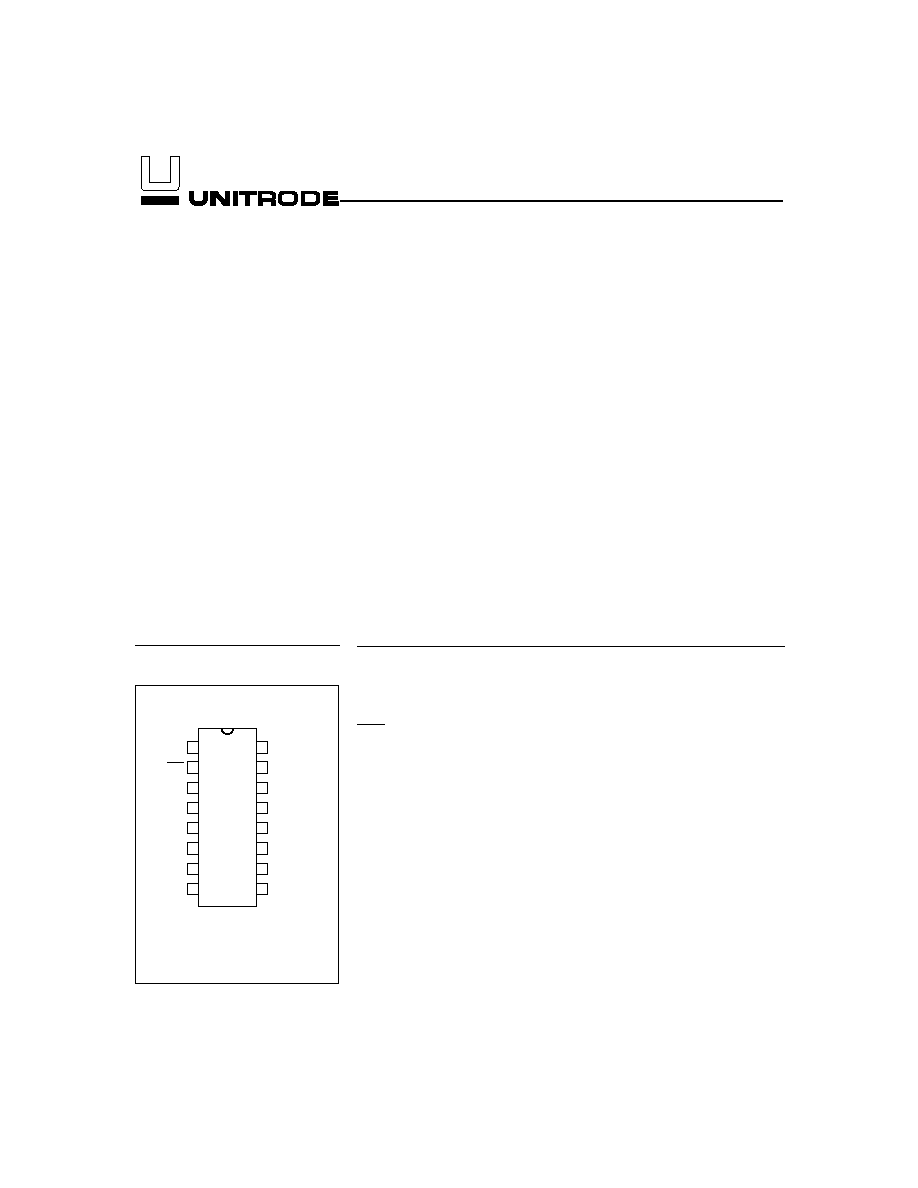
1
PN205401.eps
16-Pin Narrow
DIP or SOIC
2
3
4
5
6
7
8
16
15
14
13
12
11
10
9
LED2/DSEL
LED1
MOD
VCC
VSS
LCOM
LED3
TPWM
TM
ICTL
BAT
VCOMP
ICOMP
ITERM
SNS
TS
TPWM
Regulator timebase input
LED
3
Charge status output 3
LCOM
Common LED output
V
SS
System ground
V
CC
5.0V
±10% power
MOD
Modulation control output
LED
1
Charge status output 1
LED
2
/
Charge status output 2/
DSEL
Display select input
Pin Connections
Pin Names
6/99 H

Pin Descriptions
TM
Time-out programming input
This input sets the maximum charge time.
The resistor and capacitor values are deter-
mined using Equation 5. Figure 7 shows the
resistor/capacitor connection.
ICTL
Inrush current control output
ICTL is driven low during the fault or
charge-complete states of the chip. It is used
to disconnect the capacitor across the battery
pack terminals, preventing inrush currents
from tripping overcurrent protection fea-
tures in the pack when a new battery is in-
serted.
BAT
Battery voltage input
BAT is the battery voltage sense input. This
potential is generally developed using a
high-impedance resistor divider network
connected between the positive and the
negative terminals of the battery. See Fig-
ure 4 and Equation 1.
VCOMP
Voltage loop compensation input
This input uses an external R-C network for
voltage loop stability.
I
TERM
Minimum current termination select
This three-state input is used to set I
MIN
for
fast charge termination. See Table 2.
ICOMP
Current loop compensation input
This input uses an external R-C network for
current loop stability.
SNS
Charging current sense input
Battery current is sensed via the voltage de-
veloped on this pin by an external sense re-
sistor, R
SNS
, connected in series with the
negative terminal of the battery pack. See
Equation 6.
TS
Temperature sense input
This input is used to monitor battery tempera-
ture. An external resistor divider network sets
the lower and upper temperature thresholds.
See Figure 6 and Equations 3 and 4.
TPWM
Regulation timebase input
This input uses an external timing capacitor
to ground to set the pulse-width modulation
(PWM) frequency. See Equation 7.
LCOM
Common LED output
Common output for LED
1≠3
. This output is
in a high-impedance state during initiali-
z a t i o n t o r e a d programming input on
DSEL.
MOD
Current-switching control output
MOD is a pulse-width modulated push/pull
output that is used to control the charging
current to the battery. MOD switches high
to enable current flow and low to inhibit cur-
rent flow.
LED
1
≠
LED
3
Charger display status 1≠3 outputs
These charger status output drivers are for
the direct drive of the LED display. Display
modes are shown in Table 1. These outputs are
tri-stated during initialization so that DSEL
can be read.
DSEL
Display select input
This three-level input controls the LED
1≠3
charge display modes. See Table 1.
V
CC
V
CC
supply
5.0V,
± 10% power
V
SS
Ground
2
bq2054

Charge Algorithm
The bq2054 uses a two-phase fast charge algorithm. In
phase 1, the bq2054 regulates constant current (I
SNS
=
I
MAX
) until V
CELL
(= V
BAT
- V
SNS
) rises to V
REG
. The
bq2054 then transitions to phase 2 and regulates con-
stant voltage (V
CELL
= V
REG
) until the charging current
falls below the programmed I
MIN
threshold. The charg-
ing current must remain below I
MIN
for 120
± 40ms bef-
ore a valid fast charge termination is detected.
Fast
charge then terminates, and the bq2054 enters the
Charge Complete state. See Figures 1 and 2.
Charge Qualification
The bq2054 starts a charge cycle when power is applied
while a battery is present or when a battery is inserted.
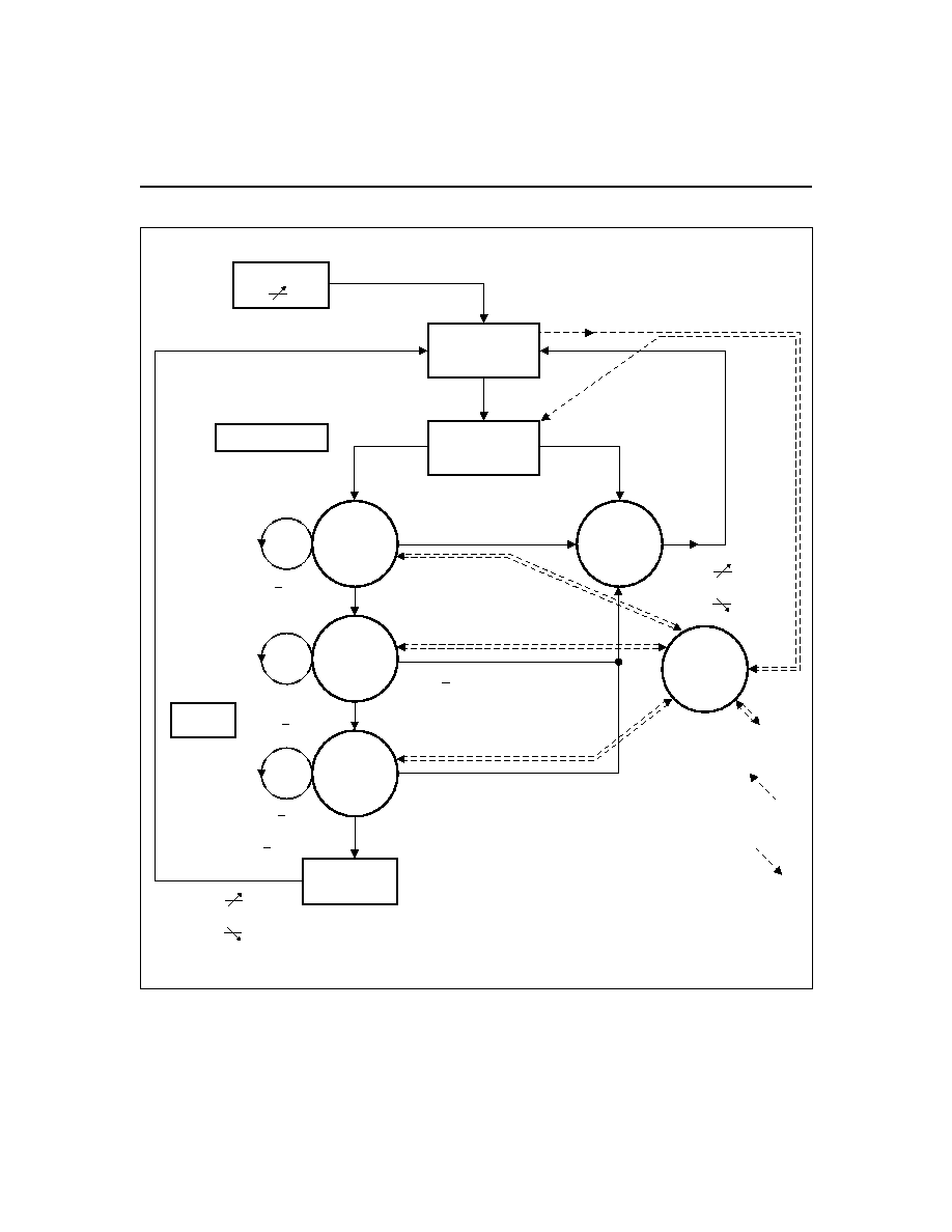
Figure 2 shows the state diagram for pre-charge qualifi-
cation and temperature monitoring. The bq2054 first
checks that the battery temperature is within the al-
lowed, user-configurable range. If the temperature is out
of range, the bq2054 enters the Charge Pending state
and waits until the battery temperature is within the al-
lowed range. Charge Pending is enunciated by LED
3
flashing.
Thermal monitoring continues throughout the charge
cycle, and the bq2054 enters the Charge Pending state
when the temperature out of range. (There is one excep-
tion; if the bq2054 is in the Fault state--see below--the
out-of-range temperature is not recognized until the
bq2054 leaves the Fault state.)
All timers are sus-
pended (but not reset) while the bq2054 is in Charge
Pending. When the temperature comes back into range,
the bq2054 returns to the point in the charge cycle
where the out-of-range temperature was detected.
When the temperature is valid, the bq2054 then regu-
lates current to I
COND
(=I
MAX
/5). After an initial holdoff
period t
HO
(which prevents the chip from reacting to
transient voltage spikes that may occur when charge
current is first applied), the chip begins monitoring
V
CELL
. If V
CELL
does not rise to at least V
MIN
before the
expiration of time-out limit t
MTO
(e.g. the cell has failed
short), the bq2054 enters the Fault state.
If V
MIN
is
achieved before expiration of the time limit, the chip be-
gins fast charging.
Once in the Fault state, the bq2054 waits until V
CC
is
cycled or a new battery insertion is detected. It then
starts a new charge cycle and begins the qualification
process again.
3
bq2054
GR205401.eps
IMAX
IMIN
ICOND
VMIN
VREG
Current
Voltage
Qualification
Time
Phase 1
Phase 2
Fast Charge
Voltage
Current
Figure 1. bq2054 Charge Algorithm
4
Chip On
VCC 4.5V
Temperature
Checks On
Battery
Status?
Temperature
in Range
Temperature Out
of Range or
Thermistor Absent
Qualification Test
Current
Regulation
@ ICOND
Phase 2
V = VREG
Fault
LED3 =1
MOD = 0
Charge
Complete
Charge
Pending
LED3 flash
MOD = 0
Phase 1
I = IMAX
Temperature Out
of Range or
Thermistor Absent
Temperature In
Range, Return
to Original State
VBAT < VLCO or
VBAT > VHCO
t t > tMTO or
VBAT < VLCO or
VBAT > VHCO
Fail: t = tQT or
VBAT < VLCO
VBAT > VHCO
Present
VLCO < VBAT < VHCO
VBAT < VMIN
PASS: VBAT VMIN
VBAT < VREG
VBAT VREG
Fast
Charge
ISNS > IMIN
ISNS IMIN
or
t tMTO
FG205401.eps
Absent
VBAT < VLCO or
VBAT > VHCO
>
>
<
>
>
VBAT VLCO
or
VBAT VHCO
VBAT VLCO
or
VBAT VHCO
Figure 2. bq2054 State Diagram
bq2054

Charge Status Display
Charge status is enunciated by the LED driver outputs
LED
1
≠LED
3
. Three display modes are available in the
bq2054; the user selects a display mode by configuring
pin DSEL. Table 1 shows the three display modes.
The bq2054 does not distinguish between an over-
voltage fault and a "battery absent" condition.
The
bq2054 enters the Fault state, enunciated by turning on
LED
3
, whenever the battery is absent.
The bq2054,
therefore, gives an indication that the charger is on even
when no battery is in place to be charged.
Configuring the Display Mode and I
MIN
DSEL/LED
2
is a bi-directional pin with two functions; it
is an LED driver pin as an output and a programming
pin as an input. The selection of pull-up, pull-down, or
no pull resistor programs the display mode on DSEL per
Table 1. The bq2054 latches the programming data
sensed on the DSEL input when any one of the following
three events occurs:
1.
V
CC
rises to a valid level.
2.
The bq2054 leaves the Fault state.
3.
The bq2054 detects battery insertion.
The LEDs go blank for approximately 750ms (typical)
while new programming data is latched.
5
bq2054
Mode
Charge Action State
LED
1
LED
2
LED
3
DSEL = 0
(Mode 1)
Battery absent or over-voltage fault
Low
Low
High
Pre-charge qualification
Flash
Low
Low
Fast charging
High
Low
Low
Charge complete
Low
High
Low
Charge pending (temperature out of range)
X
X
Flash
Charging fault
X
X
High
DSEL = 1
(Mode 2)
Battery absent or over-voltage fault
Low
Low
High
Pre-charge qualification
High
High
Low
Fast charge
Low
High
Low
Charge complete
High
Low
Low
Charge pending (temperature out of range)
X
X
Flash
Charging fault
X
X
High
DSEL = Float
(Mode 3)
Battery absent or over-voltage fault
Low
Low
High
Pre-charge qualification
Flash
Flash
Low
Fast charge: current regulation
Low
High
Low
Fast charge: voltage regulation
High
High
Low
Charge complete
High
Low
Low
Charge pending (temperature out of range)
X
X
Flash
Charging fault
X
X
High
Note:
1 = V
CC
; 0 = V
SS
; X = LED state when fault occurred; Flash =
1
6
sec. low,
1
6
sec high.
Table 1. bq2054 Display Output Summary
Fast charge terminates when the charging current drops
below a minimum current threshold programmed by the
value of I
TERM
(see Table 2) and remains below that
level for 120
± 40ms.
Figure 3 shows the bq2054 configured for display mode 2
and I
MIN
= I
MAX
/10.
Voltage and Current Monitoring
The bq2054 monitors battery pack voltage at the BAT
pin.
The user must implement a voltage divider be-
tween the positive and negative terminals of the battery
pack to present a scaled battery pack voltage to the BAT
pin. The bq2054 also uses the voltage across a sense re-
sistor (R
SNS
) between the negative terminal of the bat-
tery pack and ground to monitor the current into the
pack. See Figure 4 for the configuration of this network.
The resistor values are calculated from the following:
Equation 1
RB1
RB2
N
V
V
REG
=
-
*
.
205
1
where:
n
N = Number of cells in series
n
V
REG
= Desired fast-charging voltage per cell
These parameters are typically specified by the battery
manufacturer. The total resistance presented across the
battery pack by RB1 + RB2 should be between 150k
and 1M
. The minimum value ensures that the divider
network does not drain the battery excessively when the
power source is disconnected. Exceeding the maximum
value increases the noise susceptibility of the BAT pin.
The current sense resistor, R
SNS
(see Figure 5), deter-
mines the fast charge current.
The value of R
SNS
is
given by the following:
Equation 2
I
V
R
MAX
SNS
=
0 250
.
where:
n
I
MAX
= Desired maximum charge current
Hold-Off Period
Both V
HCO
and I
MIN
terminations are ignored during
the first 1.33
± 0.19 seconds of both the Charge Qualifi-
cation and Fast Charge phases. This condition prevents
premature termination due to voltage spikes that may
occur when charge is first applied.
6
bq2054
Table 2. I
MIN
Termination Thresholds
I
TERM
I
MIN
0
I
MAX
/10
1
I
MAX
/20
Float
I
MAX
/30

7
FG205403.eps
BAT
SNS
bq2054
7
3
13
VCC
12
BAT +
BAT -
VSS
RSNS
RB2
RB1
VSS
VCC
Figure 4. Configuring the Battery Divider
LED2/DSEL
FG205402.eps
LED1
VCC
VSS
LCOM
LED3
bq2054
11
10
12
13
15
16
6
VSS
VCC
10K
1K
1K
1K
Figure 3. Configured Display Mode/IMIN Threshold
bq2054
Battery Insertion and Removal
V
CELL
is interpreted by the bq2054 to detect the pres-
ence or absence of a battery. The bq2054 determines
that a battery is present when V
CELL
is between the
High-Voltage Cutoff (V
HCO
= V
REG
+ 0.25V) and
the Low-Voltage Cutoff (V
LCO
= 0.8V). When V
CELL
is
outside this range, the bq2054 determines that no bat-
tery is present and transitions to the Fault state. Tran-
sitions into and out of the range between V
LCO
and V
HCO
are treated as battery insertions and removals, respec-
tively. The V
HCO
limit also implicitly serves as an over-
voltage charge termination.
Inrush Current Control
Whenever the bq2054 is in the fault or charge-complete
state, the ICTL output is driven low. This output can be
used to disconnect the capacitor usually present in the
charger across the positive and negative battery termi-
nals, preventing the cap from supplying large inrush
currents to a newly inserted battery. Such inrush cur-
rents may trip the overcurrent protection circuitry usu-
ally present in Li-Ion battery packs.
Temperature Monitoring
The bq2054 monitors temperature by examining the
voltage presented between the TS and SNS pins by a re-
sistor network that includes a Negative Temperature
Coefficient (NTC) thermistor.
Resistance variations
around that value are interpreted as being proportional
to the battery temperature (see Figure 6).
The temperature thresholds used by the bq2054 and
their corresponding TS pin voltage are:
n
TCO (Temperature Cutoff): Higher limit of the tem-
perature range in which charging is allowed. V
TCO
=
0.4 * V
CC
n
HTF (High-Temperature Fault): Threshold to which
temperature must drop after temperature cutoff is
exceeded before charging can begin again.
V
HTF
=
0.44 * V
CC
n
LTF (Low-Temperature Fault):
Lower limit of the
temperature range in which charging is allowed.
V
LTF
= 0.6 * V
CC
8
VCC
VLTF = 0.6VCC
VHTF = 0.44VCC
VTCO = 0.4VCC
Hotter
VSS
TCO
HTF
LTF
Colder
V
o
lt
age
Temperature
Figure 6. Voltage Equivalent
of Temperature
SNS
bq2054
7
13
VCC
12
BAT -
VSS
RSNS
RT2
RT1
VSS
VCC
TS
8
∞t
NTC
Thermistor
RT
Figure 5. Configuring
Temperature Sensing
bq2054
A resistor-divider network can be implemented that
presents the defined voltage levels to the TS pin at the
desired temperatures (see Figure 6).
The equations for determining RT1 and RT2 are:
Equation 3
0 6
0 250
1
. *
(
.
)
* (
)
(
*
)
V
V
RT1
RT2
R
RT2
R
CC
CC
LTF
LTF
=
-
+
+
Equation 4
0 44
1
1
.
* (
)
(
*
)
=
+
+
RT1
RT2
R
RT2
R
HTF
HTF
where:
n
R
LTF
= thermistor resistance at LTF
n
R
HTF
= thermistor resistance at HTF
TCO is determined by the values of RT1 and RT2. 1%
resistors are recommended.
Disabling Temperature Sensing
Temperature sensing can be disabled by placing 10k
resistors between TS and SNS and between SNS and
V
CC
.
Maximum Time-Out
MTO is programmed from 1 to 24 hours by an R-C net-
work on the TM pin (see Figure 7) per the equation:
Equation 5
t
MTO
= 0.5 * R * C
Where R is in k
and C is in µF, t
MTO
is in hours. The
maximum value for C (0.1
µF) is typically used.
The MTO timer is reset at the beginning of fast charge
and when fast charge transitions from the current regu-
lated to the voltage regulated mode. If MTO expires dur-
ing the current regulated phase, the bq2054 enters the
Fault state and terminates charge. If the MTO timer ex-
pires during the voltage regulated phase, fast charging
terminates and the bq2054 enters the Charge Complete
state.
The MTO timer is suspended (but not reset) during the
out-of-range temperature (Charge Pending) state.
Charge Regulation
The bq2054 controls charging through pulse-width
modulation of the MOD output pin, supporting both
constant-current and constant-voltage regulation.
Charge current is monitored at the SNS pin, and charge
voltage is monitored at the BAT pin. These voltages are
compared to an internal reference, and the MOD output
modulated to maintain the desired value.
Voltage at the SNS pin is determined by the value of re-
sistor R
SNS
, so nominal regulated current is set by:
Equation 6
I
MAX
= 0.250V/R
SNS
The switching frequency of the MOD output is deter-
mined by an external capacitor (CPWM) between the
pin TPWM and ground, per the following:
Equation 7
F
PWM
= 0.1/C
PWM
Where C is in
µF and F is in kHz. A typical switching
rate is 100kHz, implying C
PWM
= 0.001
µF. MOD pulse
width is modulated between 0 and 90% of the switching
period.
To prevent oscillation in the voltage and current control
loops, frequency compensation networks (C or R-C) are typi-
cally required on the V
COMP
and I
COMP
pins (respectively).
9
TM
FG205406.eps
VCC
VSS
bq2054
12
13
1
VSS
VCC
C
R
Figure 7. R-C Network for Setting MTO
bq2054
10
Absolute Maximum Ratings
Symbol
Parameter
Minimum
Maximum
Unit
Notes
V
CC
V
CC
relative to V
SS
-0.3
+7.0
V
V
T
DC voltage applied on any pin ex-
cluding V
CC
relative to V
SS
-0.3
+7.0
V
T
OPR
Operating ambient temperature
-20
+70
∞C
Commercial
T
STG
Storage temperature
-55
+125
∞C
T
SOLDER
Soldering temperature
-
+260
∞C
10 sec. max.
Note:
Permanent device damage may occur if Absolute Maximum Ratings are exceeded. Functional opera-
tion should be limited to the Recommended DC Operating Conditions detailed in this data sheet. Expo-
sure to conditions beyond the operational limits for extended periods of time may affect device reliability.
bq2054
11
DC Thresholds
(TA = TOPR; VCC = 5V
±10%)
Symbol
Parameter
Rating
Unit
Tolerance
Notes
V
REF
Internal reference voltage
2.05
V
1%
T
A
= 25∞C
Temperature coefficient
-0.5
mV/∞C
10%
V
LTF
TS maximum threshold
0.6 * V
CC
V
±0.03V
Low-temperature fault
V
HTF
TS hysteresis threshold
0.44 * V
CC
V
±0.03V
High-temperature fault
V
TCO
TS minimum threshold
0.4 * V
CC
V
±0.03V
Temperature cutoff
V
HCO
High cutoff voltage
2.3V
V
1%
V
MIN
Under-voltage threshold at BAT
0.2 * V
CC
V
±0.03V
V
LCO
Low cutoff voltage
0.8
V
±0.03V
V
SNS
Current sense at SNS
0.250
V
10%
I
MAX
0.050
V
10%
I
COND
bq2054

12
Recommended DC Operating Conditions
(TA = TOPR)
Symbol
Parameter
Minimum
Typical
Maximum
Unit
Notes
V
CC
Supply voltage
4.5
5.0
5.5
V
V
TEMP
Temperature sense voltage
0
-
V
CC
V
V
TS
- V
SNS
V
CELL
Per cell battery voltage input
0
-
V
CC
V
V
BAT
- V
SNS
I
CC
Supply current
-
2
4
mA
Outputs unloaded
I
IZ
DSEL tri-state open detection
-2
-
2
µA
Note 2
I
TERM
tri-state open detection
-2
2
µA
V
IH
Logic input high
V
CC
-0.3
-
-
V
DSEL, I
TERM
V
IL
Logic input low
-
-
V
SS
+0.3
V
DSEL, I
TERM
V
OH
LED
1-3
, ICTL, output high
V
CC
-0.8
-
-
V
I
OH
10mA
MOD output high
V
CC
-0.8
-
-
V
I
OH
10mA
V
OL
LED
1-3
, ICTL, output low
-
-
V
SS
+0.8V
V
I
OL
10mA
MOD output low
-
-
V
SS
+0.8V
V
I
OL
10mA
LCOM output low
-
-
V
SS+
0.5
V
I
OL
30mA
I
OH
LED
1-3
, ICTL, source
-10
-
-
mA
V
OH
=V
CC
-0.5V
MOD source
-5.0
-
-
mA
V
OH
=V
CC
-0.5V
I
OL
LED
1-3
, ICTL, sink
10
-
-
mA
V
OL
= V
SS
+0.5V
MOD sink
5
-
-
mA
V
OL
= V
SS
+0.8V
LCOM sink
30
-
-
mA
V
OL
= V
SS
+0.5V
I
IL
DSEL logic input low source
-
-
+30
µA
V = V
SS
to V
SS
+ 0.3V, Note 2
I
TERM
logic input low source
-
-
+70
µA
V = V
SS
to V
SS
+ 0.3V
I
IH
DSEL logic input high source
-30
-
-
µA
V = V
CC
- 0.3V to V
CC
I
TERM
logic input high source
-70
-
-
µA
V = V
CC
- 0.3V to V
CC
Notes:
1.
All voltages relative to V
SS
except where noted.
2.
Conditions during initialization after V
CC
applied.
bq2054
13
Impedance
Symbol
Parameter
Minimum
Typical
Maximum
Unit
Notes
R
BATZ
BAT pin input impedance
50
-
-
M
R
SNSZ
SNS pin input impedance
50
-
-
M
R
TSZ
TS pin input impedance
50
-
-
M
R
PROG1
Soft-programmed pull-up or pull-down
resistor value (for programming)
-
-
10
k
DSEL
R
PROG2
Pull-up or pull-down resistor value
-
-
3
k
I
TERM
R
MTO
Charge timer resistor
20
-
480
k
Timing
(TA = TOPR; VCC = 5V
±10%)
Symbol
Parameter
Minimum
Typical
Maximum
Unit
Notes
t
MTO
Charge time-out range
1
-
24
hours
See Figure 7
t
QT
Pre-charge qual test time-out period
-
t
MTO
-
-
t
HO
Termination hold-off period
1.14
-
1.52
sec.
t
IMIN
Min. current detect filter period
80
160
msec.
F
PWM
PWM regulator frequency range
-
100
kHz
C
PWM
= 0.001
µF
(equation 7)
Capacitance
Symbol
Parameter
Minimum
Typical
Maximum
Unit
C
MTO
Charge timer capacitor
-
-
0.1
µF
C
PWM
PWM R-C capacitance
-
0.001
-
µF
bq2054
14
bq2054
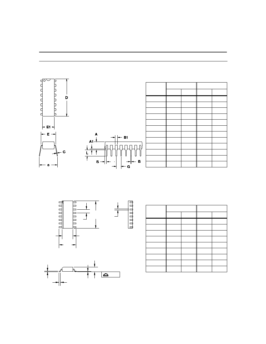
16-Pin PN (0.300" DIP)
Dimension
Inches
Millimeters
Min.
Max.
Min.
Max.
A
0.160
0.180
4.06
4.57
A1
0.015
0.040
0.38
1.02
B
0.015
0.022
0.38
0.56
B1
0.055
0.065
1.40
1.65
C
0.008
0.013
0.20
0.33
D
0.740
0.770
18.80
19.56
E
0.300
0.325
7.62
8.26
E1
0.230
0.280
5.84
7.11
e
0.300
0.370
7.62
9.40
G
0.090
0.110
2.29
2.79
L
0.115
0.150
2.92
3.81
S
0.020
0.040
0.51
1.02
16-Pin DIP Narrow (PN)
16-Pin SOIC Narrow (SN)
A
A1
.004
C
B
e
D
E
H
L
16-Pin SN (0.150" SOIC)
Dimension
Inches
Millimeters
Min.
Max.
Min.
Max.
A
0.060
0.070
1.52
1.78
A1
0.004
0.010
0.10
0.25
B
0.013
0.020
0.33
0.51
C
0.007
0.010
0.18
0.25
D
0.385
0.400
9.78
10.16
E
0.150
0.160
3.81
4.06
e
0.045
0.055
1.14
1.40
H
0.225
0.245
5.72
6.22
L
0.015
0.035
0.38
0.89
15
bq2054
Data Sheet Revision History
Change No. Page No.
Description
Nature of Change
1
5, 7, 8, 10 Value Change
Changed V
SNS
and I
MAX
2
5, 10
Value Change
Changed V
REF
3
10
Coefficient Addition
Temperature coefficient added
4
5
New state diagram
Diagram inserted
4
1, 2, 8, 12
NC pin replaced with ICTL
4
3, 5, 13
Termination hold-off period added
I
MIN
detect filtering added
5
11
V
HCO
Rating changed to 2.3V
V
HCO
Tolerance changed to 1%
Changed values for V
HCO
6
13
t
QT
in Timing Specifications
t
QT
changed from (0.16
t
MTO
) to t
MTO
7
5
I
TERM
in Table 2
Z changes to Float
7
8
Figure 6
RB1 and RB2 changed to RT1 and RT2
8
10
T
OPR
Deleted industrial temperature range.
Notes:
Change 3 = April 1996 C changes from Dec. 1995 B.
Change 4 = Sept. 1996 D changes from April 1996 C.
Change 5 = Nov. 1996 E changes from Sept. 1996 D.
Change 6 = Oct. 1997 F changes from Nov. 1996 E.
Change 7 = Oct. 1997 G changes from Oct. 1997 F.
Change 8 = June 1999 H changes from Oct. 1997 G.
Ordering Information
bq2054
Package Option:
PN = 16-pin plastic DIP
SN = 16-pin narrow SOIC
Device:
bq2054 Li-Ion Fast-Charge IC

IMPORTANT NOTICE
Texas Instruments and its subsidiaries (TI) reserve the right to make changes to their products or to discontinue
any product or service without notice, and advise customers to obtain the latest version of relevant information
to verify, before placing orders, that information being relied on is current and complete. All products are sold
subject to the terms and conditions of sale supplied at the time of order acknowledgement, including those
pertaining to warranty, patent infringement, and limitation of liability.
TI warrants performance of its semiconductor products to the specifications applicable at the time of sale in
accordance with TI's standard warranty. Testing and other quality control techniques are utilized to the extent
TI deems necessary to support this warranty. Specific testing of all parameters of each device is not necessarily
performed, except those mandated by government requirements.
CERTAIN APPLICATIONS USING SEMICONDUCTOR PRODUCTS MAY INVOLVE POTENTIAL RISKS OF
DEATH, PERSONAL INJURY, OR SEVERE PROPERTY OR ENVIRONMENTAL DAMAGE ("CRITICAL
APPLICATIONS"). TI SEMICONDUCTOR PRODUCTS ARE NOT DESIGNED, AUTHORIZED, OR
WARRANTED TO BE SUITABLE FOR USE IN LIFE-SUPPORT DEVICES OR SYSTEMS OR OTHER
CRITICAL APPLICATIONS. INCLUSION OF TI PRODUCTS IN SUCH APPLICATIONS IS UNDERSTOOD TO
BE FULLY AT THE CUSTOMER'S RISK.
In order to minimize risks associated with the customer's applications, adequate design and operating
safeguards must be provided by the customer to minimize inherent or procedural hazards.
TI assumes no liability for applications assistance or customer product design. TI does not warrant or represent
that any license, either express or implied, is granted under any patent right, copyright, mask work right, or other
intellectual property right of TI covering or relating to any combination, machine, or process in which such
semiconductor products or services might be or are used. TI's publication of information regarding any third
party's products or services does not constitute TI's approval, warranty or endorsement thereof.
Copyright
©
1999, Texas Instruments Incorporated