 | –≠–ª–µ–∫—Ç—Ä–æ–Ω–Ω—ã–π –∫–æ–º–ø–æ–Ω–µ–Ω—Ç: BQ2201 | –°–∫–∞—á–∞—Ç—å:  PDF PDF  ZIP ZIP |
Features
Æ Power monitoring and switching
for 3-volt battery-backup applica-
tions
Æ Write-protect control
Æ 3-volt primary cell inputs
Æ Less than 10ns chip-enable
propagation delay
Æ 5% or 10% supply operation
General Description
The CMOS bq2201 SRAM Nonvolatile
Controller Unit provides all necessary
functions for converting a standard
CMOS SRAM into nonvolatile
read/write memory.
A precision comparator monitors the
5V V
CC
input for an out-of-tolerance
condition. When out of tolerance is
detected, a conditioned chip-enable
output is forced inactive to write-
protect any standard CMOS SRAM.
During a power failure, the external
SRAM is switched from the V
CC
supply to one of two 3V backup sup-
plies. On a subsequent power-up, the
SRAM is write-protected until a
power-valid condition exists.
The bq2201 is footprint- and timing-
compatible with industry stan-
dards with the added benefit of a
chip-enable propagation delay of
less than 10ns.
1
SRAM Nonvolatile Controller Unit
bq2201
Oct. 1998 D
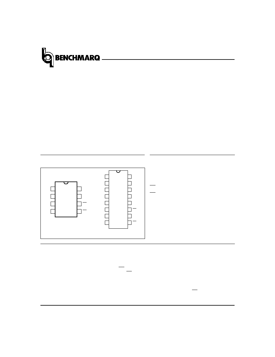
Pin Names
V
OUT
Supply output
BC
1
--BC
2
3-volt primary backup cell inputs
THS
Threshold select input
CE
chip-enable active low input
CE
CON
Conditioned chip-enable output
V
CC
+5-volt supply input
V
SS
Ground
NC
No Connect
Functional Description
Pin Connections
An external CMOS static RAM can be battery-backed
using the V
OUT
and the conditioned chip-enable output
pin from the bq2201. As V
CC
slews down during a power
failure, the conditioned chip-enable output CE
CON
is
forced inactive independent of the chip-enable input CE.
This activity unconditionally write-protects external
SRAM as V
CC
falls to an out-of-tolerance threshold V
PFD
.
V
PFD
is selected by the threshold select input pin, THS.
If THS is tied to V
SS
, power-fail detection occurs at 4.62V
typical for 5% supply operation. If THS is tied to V
CC
,
power-fail detection occurs at 4.37V typical for 10% sup-
ply operation. The THS pin must be tied to V
SS
or V
CC
for
proper operation.
If a memory access is in process during power-fail detec-
tion, that memory cycle continues to completion before the
memory is write-protected. If the memory cycle is not ter-
minated within time t
WPT
, the CE
CON
output is uncondi-
tionally driven high, write-protecting the memory.
1
PN220101.eps
8-Pin Narrow DIP or SOIC
2
3
4
8
7
6
5
VCC
BC1
CECON
CE
VOUT
BC2
THS
VSS
1
PN2201E.eps
16-Pin SOIC
2
3
4
5
6
7
8
16
15
14
13
12
11
10
9
NC
V
CC
NC
BC
1
NC
CE
CON
NC
CE
NC
V
OUT
NC
BC
2
NC
THS
NC
VSS

As the supply continues to fall past V
PFD
, an internal
switching device forces V
OUT
to one of the two external
backup energy sources. CE
CON
is held high by the V
OUT
energy source.
During power-up, V
OUT
is switched back to the V
CC
sup-
ply as V
CC
rises above the backup cell input voltage
sourcing V
OUT
. The CE
CON
output is held inactive for
time t
CER
(120 ms maximum) after the supply has
reached V
PFD
, independent of the CE input, to allow for
processor stabilization.
During power-valid operation, the CE input is fed
through to the CE
CON
output with a propagation delay
of less than 10ns. Nonvolatility is achieved by hardware
hookup, as shown in Figure 1.
Energy Cell Inputs--BC1, BC2
Two primary backup energy source inputs are provided
on the bq2201. The BC
1
and BC
2
inputs accept a 3V pri-
mary battery, typically some type of lithium chemistry.
If no primary cell is to be used on either BC
1
or BC
2
, the
unused input should be tied to V
SS
.
If both inputs are used, during power failure the V
OUT
output is fed only by BC
1
as long as it is greater than
2.5V. If the voltage at BC
1
falls below 2.5V, an internal
isolation switch automatically switches V
OUT
from BC
1
to BC
2
.
To prevent battery drain when there is no valid data to
retain, V
OUT
and CE
CON
are internally isolated from
BC
1
and BC
2
by either of the following:
s
Initial connection of a battery to BC
1
or BC
2
, or
s
Presentation of an isolation signal on CE.
A valid isolation signal requires CE low as V
CC
crosses
both V
PFD
and V
SO
during a power-down. See Figure 2.
Between these two points in time, CE must be brought
to the point of (0.48 to 0.52)*V
CC
and held for at least
700ns.
The isolation signal is invalid if CE exceeds
0.54*V
CC
at any point between V
CC
crossing V
PFD
and
V
SO
.
The appropriate battery is connected to V
OUT
and CE
CON
immediately on subsequent application and removal of V
CC
.
2
FG220101.eps
VCC
CE
BC1
THS
VSS
VOUT
CECON
BC2
bq2201
VCC
CE
CMOS
SRAM
5V
From Address Decoder
3V
Primary
Cell
3V
Primary
Cell
Figure 1. Hardware Hookup (5% Supply Operation)
Oct. 1998 D
TD220101.eps
VCC
CE
VPFD
VSO
0.5 VCC
700ns
Figure 2. Battery Isolation Signal
bq2201

3
Absolute Maximum Ratings
Symbol
Parameter
Value
Unit
Conditions
V
CC
DC voltage applied on V
CC
relative to V
SS
-0.3 to 7.0
V
V
T
DC voltage applied on any pin excluding V
CC
relative to V
SS
-0.3 to 7.0
V
V
T
V
CC
+ 0.3
T
OPR
Operating temperature
0 to +70
∞C
Commercial
-40 to +85
∞C
Industrial "N"
T
STG
Storage temperature
-55 to +125
∞C
T
BIAS
Temperature under bias
-40 to +85
∞C
T
SOLDER
Soldering temperature
260
∞C
For 10 seconds
I
OUT
V
OUT
current
200
mA
Note:
Permanent device damage may occur if Absolute Maximum Ratings are exceeded. Functional opera-
tion should be limited to the Recommended DC Operating Conditions detailed in this data sheet. Expo-
sure to conditions beyond the operational limits for extended periods of time may affect device reliability.
Recommended DC Operating Conditions
(TA = TOPR)
Symbol
Parameter
Minimum
Typical
Maximum
Unit
Notes
V
CC
Supply voltage
4.75
5.0
5.5
V
THS = V
SS
4.50
5.0
5.5
V
THS = V
CC
V
SS
Supply voltage
0
0
0
V
V
IL
Input low voltage
-0.3
-
0.8
V
V
IH
Input high voltage
2.2
-
V
CC
+ 0.3
V
V
BC1
,
V
BC2
Backup cell voltage
2.0
-
4.0
V
THS
Threshold select
-0.3
-
V
CC
+ 0.3
V
Note:
Typical values indicate operation at T
A
= 25∞C, V
CC
= 5V or V
BC
.
Oct. 1998 D
bq2201

4
DC Electrical Characteristics
(TA = TOPR, VCC = 5V
±
10%)
Symbol
Parameter
Minimum
Typical
Maximum
Unit
Conditions/Notes
I
LI
Input leakage current
-
-
±
1
µ
A
V
IN
= V
SS
to V
CC
V
OH
Output high voltage
2.4
-
-
V
I
OH
= -2.0mA
V
OHB
V
OH
, BC supply
V
BC
- 0.3
-
-
V
V
BC
> V
CC
, I
OH
= -10
µ
A
V
OL
Output low voltage
-
-
0.4
V
I
OL
= 4.0mA
I
CC
Operating supply current
-
3
5
mA
No load on V
OUT
and CE
CON
.
V
PFD
Power-fail detect voltage
4.55
4.62
4.75
V
THS = V
SS
4.30
4.37
4.50
V
THS = V
CC
V
SO
Supply switch-over voltage
-
V
BC
-
V
I
CCDR
Data-retention mode
current
-
-
100
nA
V
OUT
data-retention current
to additional memory not in-
cluded.
V
OUT1
V
OUT
voltage
V
CC
- 0.2
-
-
V
V
CC
> V
BC
, I
OUT
= 100mA
V
CC
- 0.3
-
-
V
V
CC
> V
BC
, I
OUT
= 160mA
V
OUT2
V
OUT
voltage
V
BC
- 0.3
-
-
V
V
CC
< V
BC
, I
OUT
= 100
µ
A
V
BC
Active backup cell
voltage
-
V
BC2
-
V
V
BC1
< 2.5V
-
V
BC1
-
V
V
BC1
> 2.5V
I
OUT1
V
OUT
current
-
-
160
mA
V
OUT
> V
CC
- 0.3V
I
OUT2
V
OUT
current
-
100
-
µ
A
V
OUT
> V
BC
- 0.2V
Note:
Typical values indicate operation at T
A
= 25∞C, V
CC
= 5V or V
BC
.
Oct. 1998 D
bq2201
5
AC Test Conditions
Parameter
Test Conditions
Input pulse levels
0V to 3.0V
Input rise and fall times
5ns
Input and output timing reference levels
1.5V (unless otherwise specified)
Output load (including scope and jig)
See Figure 3
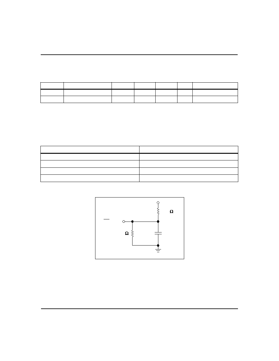
FG220102.eps
5V
960
100pF
CECON
510
Figure 3. Output Load
Capacitance
(TA = 25∞C, F = 1MHz, VCC = 5.0V)
Symbol
Parameter
Minimum
Typical
Maximum
Unit
Conditions
C
IN
Input capacitance
-
-
8
pF
Input voltage = 0V
C
OUT
Output capacitance
-
-
10
pF
Output voltage = 0V
Note:
This parameter is sampled and not 100% tested.
Oct. 1998 D
bq2201