 | –≠–ª–µ–∫—Ç—Ä–æ–Ω–Ω—ã–π –∫–æ–º–ø–æ–Ω–µ–Ω—Ç: BQ2202 | –°–∫–∞—á–∞—Ç—å:  PDF PDF  ZIP ZIP |

Features
‰ Power monitoring and switching
for nonvolatile control of SRAMs
‰ Write-protect control
‰ Input decoder allows control of
up to 2 banks of SRAM
‰ 3-volt primary cell input
‰ 3-volt rechargeable battery in-
put/output
‰ Reset output for system power-on
reset
‰ Less than 10ns chip enable
propagation delay
‰ 5% or 10% supply operation
General Description
The CMOS bq2202 SRAM Nonvolatile
Controller With Reset provides all the
necessary functions for converting one
or two banks of standard CMOS
SRAM into nonvolatile read/write
memory.
A precision comparator monitors the
5V V
CC
input for an out-of-tolerance
condition. When out-of-tolerance is
d e t e c t e d , t h e t w o c o n d i t i o n e d
chip-enable outputs are forced inac-
tive to write-protect both banks of
SRAM.
Power for the external SRAMs is
switched from the V
CC
supply to the
battery-backup supply as V
CC
de-
cays. On a subsequent power--up, the
V
OUT
supply is automatically
switched from the backup supply to
the V
CC
supply. The external SRAMs
are write-protected until a power-
valid condition exists. The reset out-
put provides power-fail and power-on
resets for the system.
During power-valid operation, the
input decoder selects one of two
banks of SRAM.
1
Pin Names
V
OUT
Supply output
RST
Reset output
THS
Threshold select input
CE
Chip enable active low input
CE
CON1
,
Conditioned chip enable outputs
CE
CON2
A
Bank select input
BC
P
3V backup supply input
BC
S
3V rechargeable backup supply input/output
NC
No connect
V
CC
+5 volt supply input
V
SS
Ground
Two banks of CMOS static RAM can be battery-backed
using the V
OUT
and conditioned chip-enable output pins
from the bq2202. As the voltage input V
CC
slews down
during a power failure, the two conditioned chip enable
outputs, CE
CON1
and CE
CON2
, are forced inactive
independent of the chip enable input CE.
This activity unconditionally write-protects external
SRAM as V
CC
falls to an out-of-tolerance threshold
V
PFD
. V
PFD
is selected by the threshold select input pin,
THS. If THS is tied to V
SS
, the power-fail detection oc-
curs at 4.62V typical for 5% supply operation.
If THS is tied to V
CC
, power-fail detection occurs at
4.37V typical for 10% supply operation. The THS pin
must be tied to V
SS
or V
CC
for proper operation.
If a memory access is in process to any of the two exter-
nal banks of SRAM during power-fail detection, that
memory cycle continues to completion before the memory
is write-protected. If the memory cycle is not terminated
within time t
WPT
(150
µ
sec maximum), the two chip en-
able outputs are unconditionally driven high, write-
protecting the controlled SRAMs.
SRAM NV Controller With Reset
bq2202
Sept. 1997 D
1
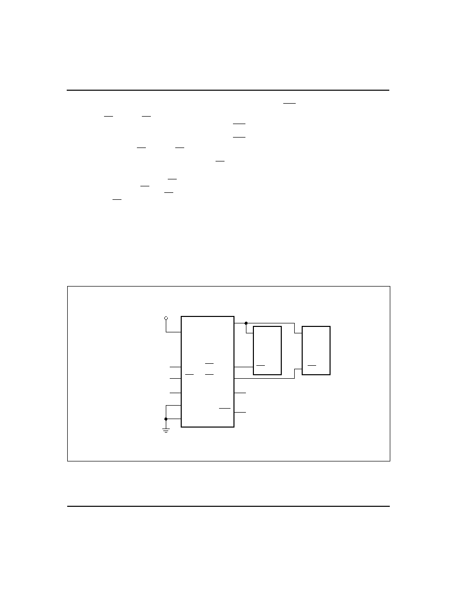
PN220201.eps
16-Pin Narrow DIP or SOIC
2
3
4
5
6
7
8
16
15
14
13
12
11
10
9
VCC
BCS
CE
CECON1
CECON2
NC
RST
NC
VOUT
BCP
NC
A
NC
NC
THS
VSS
Functional Description
Pin Connections
As the supply continues to fall past V
PFD
, an internal
switching device forces V
OUT
to the internal backup en-
ergy source. CE
CON1
and CE
CON2
are held high by the
V
OUT
energy source.
During power-up, V
OUT
is switched back to the 5V sup-
ply as V
CC
rises above the backup cell input voltage
sourcing V
OUT
. Outputs CE
CON1
and CE
CON2
are held
inactive for time t
CER
(120ms maximum) after the
power supply has reached V
PFD
, independent of the CE
input, to allow for processor stabilization.
During power-valid operation, the CE input is passed
through to one of the two CE
CON
outputs with a propa-
gation delay of less than 10ns. The CE input is output on
one of the two CE
CON
output pins; depending on the
level of bank select input A, as shown in the Truth Ta-
ble.
Bank select input A is usually tied to a high-order ad-
dress pin so that a large nonvolatile memory can be de-
signed using lower-density memory devices. Nonvolatility
and decoding are achieved by hardware hookup as shown
in Figure 1.
The reset output (RST) goes active within t
PFD
(150
µ
sec
maximum) after V
PFD,
and remains active for a minimum
of 40ms (120ms maximum) after power returns valid. The
RST output can be used as the power-on reset for a micro-
processor. Access to the external RAM may begin when
RST returns inactive.
Energy Cell Inputs--BC
P
, BC
S
Two backup energy source inputs are provided on the
bq2202--a primary cell BC
P
and a secondary cell BC
S
.
The primary cell input is designed to accept any 3V pri-
mary battery (non-rechargeable), typically some type of
lithium chemistry. If a primary cell is not to be used, the
BC
P
pin should be grounded. The secondary cell input
BC
S
is designed to accept constant-voltage current-
limited rechargeable cells.
During normal 5V power valid operation, 3.3V is output
on the BC
S
pin and is current-limited internally.
2
FG220201.eps
VCC
CE
BCP
THS
VSS
VOUT
bq2202
VCC
CE
CMOS
SRAM
5V
From Address
Decoder
CECON2
BCS
RST
CECON1
A
VCC
CE
CMOS
SRAM
To Microprocessor
Figure 1. Hardware Hookup (5% Supply Operation)
Sept. 1997 D
bq2202

If a secondary cell is not to be used, the BC
S
pin must be
tied directly to V
SS
. If both inputs are used, during
power failure the V
OUT
and CE
CON
outputs are forced
high by the secondary cell so long as it is greater than
2.5V. Only the secondary cell is loaded by the data reten-
tion current of the SRAM until the voltage at the BC
S
pin falls below 2.5V. When and if the voltage at BC
S
falls below 2.5V, an internal isolation switch automati-
cally transfers the load from the secondary cell to the
primary cell.
To prevent battery drain when there is no valid data to
retain, V
OUT
, CE
CON1
, and CE
CON2
are internally iso-
lated from BC
P
and BC
S
by either:
s
Initial connection of a battery to BC
P
or BC
S
or
s
Presentation of an isolation signal on CE.
A valid isolation signal requires CE low as V
CC
crosses
both V
PFD
and V
SO
during a power-down. See Figure
2.
Between these two points in time, CE must be
brought to V
CC
(0.48 to 0.52) and held for at least
700ns. The isolation signal is invalid if CE exceeds V
CC
*
0.54 at any point between V
CC
crossing V
PFD
and V
SO
.
The battery is connected to V
OUT
, CE
CON1
, and
CE
CON2
immediately on subsequent application and
removal of V
CC
.
3
TD220201.eps
VCC
CE
VPFD
VSO
0.5 VCC
700ns
Figure 2. Battery Isolation Signal
Truth Table
Input
Output
CE
A
CE
CON1
CE
CON2
H
X
H
H
L
L
L
H
L
H
H
L
Sept. 1997 D
bq2202

4
Recommended DC Operating Conditions
(TA = TOPR)
Symbol
Parameter
Minimum
Typical
Maximum
Unit
Notes
V
CC
Supply voltage
4.75
5.0
5.5
V
THS = V
SS
4.50
5.0
5.5
V
THS = V
CC
V
BCP
Backup cell input voltage
2.0
-
4.0
V
V
CC
< V
BC
V
BCS
2.5
-
4.0
V
SS
Supply voltage
0
0
0
V
V
IL
Input low voltage
-0.3
-
0.8
V
V
IH
Input high voltage
2.2
-
V
CC
+ 0.3
V
THS
Threshold select
-0.3
-
V
CC
+ 0.3
V
Note:
Typical values indicate operation at T
A
= 25∞C, V
CC
= 5V or V
BC
.
Absolute Maximum Ratings
Symbol
Parameter
Value
Unit
Conditions
V
CC
DC voltage applied on V
CC
relative to V
SS
-0.3 to +7.0
V
V
T
DC voltage applied on any pin excluding V
CC
relative to V
SS
-0.3 to +7.0
V
V
T
V
CC
+ 0.3
T
OPR
Operating temperature
0 to +70
∞C
Commercial
-40 to +85
∞C
Industrial "N"
T
STG
Storage temperature
-55 to +125
∞C
T
BIAS
Temperature under bias
-40 to +85
∞C
T
SOLDER
Soldering temperature
260
∞C
For 10 seconds
I
OUT
V
OUT
current
200
mA
Note:
Permanent device damage may occur if Absolute Maximum Ratings are exceeded. Functional opera-
tion should be limited to the Recommended DC Operating Conditions detailed in this data sheet. Expo-
sure to conditions beyond the operational limits for extended periods of time may affect device reliability.
Sept. 1997 D
bq2202

5
DC Electrical Characteristics
(TA = TOPR, VCC = 5V
±
10%)
Symbol
Parameter
Minimum
Typical
Maximum
Unit
Conditions/Notes
I
LI
Input leakage current
-
-
±
1
µ
A
V
IN
= V
SS
to V
CC
V
OH
Output high voltage
2.4
-
-
V
I
OH
= -2.0mA
V
OHB
V
OH
, backup supply
V
BC
- 0.3
-
-
V
V
BC
> V
CC
, I
OH
= -10
µ
A
V
OL
Output low voltage
-
-
0.4
V
I
OL
= 4.0mA
I
CC
Operating supply current
-
3
6
mA
No load on V
OUT
, CE
CON1
,
and CE
CON2
V
PFD
Power-fail detect voltage
4.55
4.62
4.75
V
THS = V
SS
4.30
4.37
4.50
V
THS = V
CC
V
SO
Supply switch-over voltage
-
V
BC
-
V
I
CCDR
Data-retention mode
current
-
-
100
nA
No load on V
OUT
, CE
CON1
,
and CE
CON2
V
OUT1
V
OUT
voltage
V
CC
- 0.2
-
-
V
V
CC
> V
BC
, I
OUT
= 100mA
V
CC
- 0.3
-
-
V
V
CC
> V
BC
, I
OUT
= 160mA
V
OUT2
V
OUT
voltage
V
BC
- 0.2
-
-
V
V
CC
< V
BC
, I
OUT
= 100
µ
A
V
BC
Active backup cell voltage
-
V
BCS
-
V
V
BCS
> 2.5V
-
V
BCP
-
V
V
BCS
< 2.5V
R
BCS
BC
S
charge output internal
resistance
500
1000
1750
V
BCSO
3.0V
V
BCSO
BC
S
charge output voltage
3.0
3.3
3.6
V
V
CC
> V
PFD
, RST inactive,
full charge or no load
I
OUT1
V
OUT
current
-
-
160
mA
V
OUT
V
CC
- 0.3V
I
OUT2
V
OUT
current
-
100
-
µ
A
V
OUT
V
BC
- 0.2V
Note:
Typical values indicate operation at T
A
= 25∞C, V
CC
= 5V or V
BC
.
Capacitance
(TA = 25∞C, F = 1MHz, VCC = 5.0V)
Symbol
Parameter
Minimum
Typical
Maximum
Unit
Conditions
C
IN
Input capacitance
-
-
8
pF
Input voltage = 0V
C
OUT
Output capacitance
-
-
10
pF
Output voltage = 0V
Note:
This parameter is sampled and not 100% tested.
Sept. 1997 D
bq2202