 | –≠–ª–µ–∫—Ç—Ä–æ–Ω–Ω—ã–π –∫–æ–º–ø–æ–Ω–µ–Ω—Ç: BQ24026 | –°–∫–∞—á–∞—Ç—å:  PDF PDF  ZIP ZIP |
Document Outline
- FEATURES
- APPLICATIONS
- DESCRIPTION
- ORDERING INFORMATION
- DISSIPATION RATINGS
- ABSOLUTE MAXIMUM RATINGS
- RECOMMENDED OPERATING CONDITIONS(1)
- ELECTRICAL CHARACTERISTICS
- TERMINAL FUNCTIONS
- FUNCTIONAL BLOCK DIAGRAM
- TYPICAL CHARACTERISTICS
- FUNCTIONAL DESCRIPTION
- AUTONOMOUS POWER SOURCE SELECTION
- TEMPERATURE QUALIFICATION (bq24020, bq24024, bq24025, and bq24026 only)
- BATTERY PRE-CONDITIONING
- BATTERY CHARGE CURRENT
- BATTERY VOLTAGE REGULATION
- CHARGE TAPER DETECTION, TERMINATION AND RECHARGE
- NOTE ON bq24026
- SLEEP MODE
- CHARGE STATUS OUTPUTS
- PG\ OUTPUT
- CE\ INPUT (CHARGE ENABLE)
- TTE\ INPUT (TIMER AND TERMINATION ENABLE)
- THERMAL SHUTDOWN AND PROTECTION
- TE\ INPUT (TIMER ENABLED)
- TIMER FAULT RECOVERY
- APPLICATION INFORMATION
- THERMAL CONSIDERATIONS
- PCB LAYOUT CONSIDERATIONS
bq24020, bq24022,
bq24023, bq24024
bq24025, bq24026
SLUS549C - DECEMBER 2002 - REVISED AUGUST 2004
SINGLE CHIP, LI ION AND LI POL CHARGER IC WITH AUTONOMOUS
USB PORT AND AC ADAPTER SUPPLY MANAGEMENT (bqTINYt II)
FEATURES
D
Small 3 mm
◊
3 mm MLP Package
D
Charges and Powers Systems from Either AC
Adapter or USB With Autonomous
Power-Source Selection
D
Integrated USB Control With Selectable
100 mA and 500 mA Charge Rates
D
Ideal for Low-Dropout Charger Designs for
Single-Cell Li-Ion or Li-Pol Packs in Space
Limited Portable Applications
D
Integrated Power FET and Current Sensor for
Up to 1-A Charge Applications From AC
Adapter
D
Precharge Conditioning With Safety Timer
D
Power Good (AC Adapter Present) Status
Output
D
Optional Battery Temperature Monitoring
Before and During Charge
D
Automatic Sleep Mode for Low-Power
Consumption
APPLICATIONS
D
PDAs, MP3 Players
D
Digital Cameras
D
Internet Appliances
D
Smartphones
DESCRIPTION
The bqTINY-II series are highly integrated and flexible
Li-Ion linear charge and system power management
devices targeted at space limited charger applications.
The bqTINY-II series offer integrated USB-port and
ac-adapter supply management with autonomous
power-source selection, power FET and current
sensor, high-accuracy current and voltage regulation,
charge status, and charge termination, in a single
monolithic device.
The bqTINY-II automatically selects the USB-Port or
the ac-adapter as the power source for the system. In
the USB configuration, the host can select from the two
preset charge rates of 100 mA and 500 mA. In the
ac-adapter configuration an external resistor sets the
magnitude of the system or charge current.
The bqTINY-II charges the battery in three phases:
conditioning, constant current, and constant voltage.
Charge is terminated based on minimum current. An
internal charge timer provides a backup safety for
charge termination. The bqTINY-II automatically re-
starts the charge if the battery voltage falls below an
internal threshold. The bqTINY-II automatically enters
sleep mode when both supplies are removed.
bqTINY is a trademark of Texas Instruments Incorporated.
PRODUCTION DATA information is current as of publication date. Products
conform to specifications per the terms of Texas Instruments standard warranty.
Production processing does not necessarily include testing of all parameters.
Please be aware that an important notice concerning availability, standard warranty, and use in critical applications of Texas Instruments
semiconductor products and disclaimers thereto appears at the end of this data sheet.
www.ti.com
Copyright
2002, Texas Instruments Incorporated
1
2
3
4
10
9
8
5
AC
USB
OUT
VSS
STAT1
STAT2
7
6
TS
ISET2
ISET1
bq24020DRC
+
BATTERY PACK
PACK+
PACK-
SYSTEM
SYSTEM
INTERFACE
VDC
GND
VBUS
GND
D+
D -
USB
PORT
AC
ADAPTER
UDG-02184
RSET
CE

bq24020, bq24022,
bq24023, bq24024
bq24025, bq24026
SLUS549C - DECEMBER 2002 - REVISED AUGUST 2004
www.ti.com
2
DESCRIPTION (CONTINUED)
In addition to the standard features, different versions of the bqTINY-II offer a multitude of additional features. These include
temperature sensing input for detecting hot or cold battery packs; power good (PG) output indicating the presence of input
power; a TTL-level charge enable input (CE) used to disable or enable the charge process; and a TTL-level timer and
taper-detect enable (TTE) input used to disable or enable the fast-charge timer and charge termination.
These devices have limited built-in ESD protection. The leads should be shorted together or the device placed in conductive foam during
storage or handling to prevent electrostatic damage to the MOSFET gates.
ORDERING INFORMATION
TJ
CHARGE
REGULATION
VOLTAGE (V)(1)
OPTIONAL
FUNCTIONS(1)
FAST-
CHARGE
TIMER
(Hours)
TAPER
TIMER
USB TAPER
THRESHOLD
PART
NUMBER(2)
MARKINGS
4.2
CE and TS
5
Yes
10% of ISET1 Level
bq24020DRCR
AZS
4.2
PG and CE
5
Yes
10% of ISET1 Level
bq24022DRCR
AZU
4.2
CE and TTE
5
Yes
10% of ISET1 Level
bq24023DRCR
AZV
-40
∞
C to 125
∞
C
4.2
TTE and TS
5
Yes
10% of ISET1 Level
bq24024DRCR
AZW
-40 C to 125 C
4.2
CE and TS
7
Yes
10% of ISET1 Level
bq24025DRCR
AZX
4.2
TE and TS
7
No
10% of selected
USB charge rate
bq24026DRCR
ANR
(1) The DRC package is available taped and reeled only in quantities of 3,000 devices per reel.
DISSIPATION RATINGS
PACKAGE
JA
TA < 40
∞
C
POWER RATING
DERATING FACTOR
ABOVE TA = 25
∞
C
DRC(1)
46.87
∞
C/W
1.5 W
0.021 W/
∞
C
(1) This data is based on using the JEDEC High-K board and the exposed die pad is connected to a copper pad on the board. This is connected to the
ground plane by a 2x3 via matrix.
ABSOLUTE MAXIMUM RATINGS
over operating free-air temperature range unless otherwise noted(1)
bq24020, bq24022
bq24023, bq24024
bq24025, bq24026
UNITS
Input voltage(2)
AC, CE, ISET1, ISET2, OUT, PG, STAT1, STAT2,
TE, TS, TTE, USB
-0.3 to 7.0
V
Output sink/source current
STAT1, STAT2, PG
15
mA
Output current
TS
200
µ
A
Output current
OUT
1.5
A
Operating free-air temperature range, TA
-40 to 125
Junction temperature range, TJ
-40 to 125
∞
C
Storage temperature, Tstg
-65 to 150
∞
C
Lead temperature 1,6 mm (1/16 inch) from case for 10 seconds
300
(1) Stresses beyond those listed under "absolute maximum ratings" may cause permanent damage to the device. These are stress ratings only, and
functional operation of the device at these or any other conditions beyond those indicated under "recommended operating conditions" is not
implied. Exposure to absolute-maximum-rated conditions for extended periods may affect device reliability.
(2) All voltages are with respect to VSS.
RECOMMENDED OPERATING CONDITIONS
(1)
MIN
NOM
MAX
UNIT
Supply voltage (from AC input), VCC
4.5
6.5
V
Supply voltage (from USB input), VCC
4.35
6.5
V
Operating junction temperature range, TJ
-40
125
∞
C

bq24020, bq24022,
bq24023, bq24024
bq24025, bq24026
SLUS549C - DECEMBER 2002 - REVISED AUGUST 2004
www.ti.com
3
ELECTRICAL CHARACTERISTICS
over 0
_
C
TJ
125
_
C and recommended supply voltage, unless otherwise noted
PARAMETER
TEST CONDITIONS
MIN
TYP
MAX
UNIT
INPUT CURRENT
VCC current, ICC(VCC)
VCC > VCC(min)
1.2
2.0
mA
Sleep current, ICC(SLP)
Sum of currents into OUT pin,
VCC < V(SLP)
2
5
Standby current, ICC(STBY)
CE = High,
0
_
C
TJ
85
_
C
150
Input current on OUT pin, IIB(OUT)
Charge DONE,
VCC > VCC(MIN)
1
5
µ
A
Input current on CE pin, IIB(CE)
1
µ
A
Input bias current on TTE pin, IIB(TTE)
1
Input bias current on TE pin, IIB(TE)
1
VOLTAGE REGULATION VO(REG) + V(DO-MAX)
VCC , I(TERM) < IO(OUT)
1 A
Output voltage, VO(REG)
4.20
V
Voltage regulation accuracy
TA = 25
_
C
-0.35%
0.35%
Voltage regulation accuracy
-1%
1%
AC dropout voltage (V(AC)-V(OUT)), V(DO)
VO(OUT) = VO(REG), IO(OUT) = 1A
VO(REG) + V(DO-MAX))
VCC,
350
500
USB dropout voltage (V(USB) - V(OUT)),
VO(OUT) = VO(REG) ISET2 = High
VO(REG) + V(DO-MAX))
VCC,
350
500
mV
USB dropout voltage (V(USB) - V(OUT)),
V(DO)
VO(OUT) = VO(REG) ISET2 = Low
VO(REG) + V(DO-MAX))
VCC,
60
100
CURRENT REGULATION
AC output current range, IO(OUT)(1)
VI(OUT) > V(LOWV), VI(AC) - VI(OUT) > V(DO-MAX),
VCC
4.5 V,
50
1000
USB output current range, IO(OUT)
VCC(MIN)
4.5 V, VI(OUT) > V(LOWV),
VUSB - VI(OUT) > V(DO-MAX), ISET2 = Low
80
100
mA
USB output current range, IO(OUT)
VCC(MIN)
4.5 V, VI(OUT) > V(LOWV),
VUSB - VI(OUT) > V(DO-MAX), ISET2 = High
400
500
Output current set voltage, V(SET)
Voltage on ISET1 pin, VCC
4.5 V, VIN
4.5 V,
VI(OUT) > V(LOWV), VIN - VI(OUT) > V(DO-MAX)
2.463
2.500
2.538
V
50 mA
IO(OUT)
1 A
307
322
337
Output current set factor, K(SET)
10 mA
IO(OUT) < 50 mA
296
320
346
Output current set factor, K(SET)
1 mA
IO(OUT) < 10 mA
246
320
416
PRECHARGE AND SHORT-CIRCUIT CURRENT REGULATION
Precharge to fast-charge transition
threshold, V(LOWV)
Voltage on OUT pin
2.8
3.0
3.2
V
Deglitch time for fast-charge to precharge
transition
VCC(MIN)
4.5 V, tFALL = 100 ns, 10 mV overdrive
VI(OUT) decreasing below threshold
250
375
500
ms
Precharge range, IO(PRECHG)(2)
0 V < VI(OUT) < V(LOWV), t < t(PRECHG)
5
100
mA
Precharge set voltage, V(PRECHG)
Voltage on ISET1 pin, VO(REG) = 4.2 V,
0 V < VI(OUT) > V(LOWV), t < t(PRECHG)
240
255
270
mV
(1)
I
O(OUT)
+
K
(SET)
V
(SET)
R
SET
(2)
I
O(PRECHG)
+
K
(SET)
V
(PRECHG)
R
SET

bq24020, bq24022,
bq24023, bq24024
bq24025, bq24026
SLUS549C - DECEMBER 2002 - REVISED AUGUST 2004
www.ti.com
4
ELECTRICAL CHARACTERISTICS(continued)
over 0
_
C
TJ
125
_
C and recommended supply voltage, unless otherwise noted
PARAMETER
UNIT
MAX
TYP
MIN
TEST CONDITIONS
CHARGE TAPER AND TERMINATION DETECTION
Charge taper detection range, I(TAPER)(3)
VI(OUT) > V(RCH),
t < t(TAPER)
5
100
USB-100 charge taper
detection level
bq24026
VI(OUT) > V(RCH),
ISET2 = Low
6.5
9
11
mA
USB-500 charge taper
detection level
bq24026
VI(OUT) > V(RCH),
ISET2 = High
32
44
55
mA
Charge taper detection set voltage,
V(TAPER)
Voltage on ISET1 pin,
VO(REG) = 4.2 V,
VI(OUT) > V(RCH),
t < t(TAPER)
235
250
265
mV
Charge termination detection set voltage,
V(TERM)(4)
Voltage on ISET pin,
VO(REG) = 4.2 V,
VI(OUT) > V(RCH)
11
18
25
mV
Deglitch time for TAPER detection,
tTPRDET
VCC(MIN)
4.5 V,
tFALL = 100 ns
charging current increasing or decreasing above
and below,
10 mV overdrive
250
375
500
ms
Deglitch time for termination detection,
tTRMDET
VCC(MIN)
4.5 V,
tFALL = 100 ns
charging current decreasing below,
10 mV overdrive
250
375
500
ms
TEMPERATURE SENSE COMPARATOR
Low-voltage threshold, V(LTF)
2.475
2.500
2.525
V
High-voltage threshold, V(HTF)
0.485
0.500
0.515
V
Current source, I(TS)
96
102
108
µ
A
Deglitch time for temperature fault, t(DEGL)
250
375
500
ms
BATTERY RECHARGE THRESHOLD
Recharge threshold, VRCH
VO(
REG
)
-0.115
VO(
REG
)
-0.10
VO(
REG
)
-0.085
V
Deglitch time for recharge detect, t(DEGL)
VCC(MIN)
4.5 V,
tFALL = 100 ns
decreasing below or increasing above threshold,
10 mV overdrive
250
375
500
ms
STAT1, STAT2, and PG OUTPUTS
Low-level output saturation voltage, VOL
IO = 5 mA
0.25
V
ISET2, CHARGE ENABLE (CE), TIMER AND TERMINATION ENABLE (TTE), AND TIMER ENABLE (TE) INPUTS
Low-level input voltage, VIL
IIL = 10
µ
A
0
0.4
V
High-level input voltage, VIH
IIL = 20
µ
A
1.4
V
CE, TE or TTE low-level input current, IIL
-1
CE, TE or TTE high-level input current, IIH
1
µ
A
ISET2 low-level input current, IIL
IISET2 = 0
-20
µ
A
ISET2 high-level input current, IIH
IISET2 = VCC
40
ISET2 high-Z input current, IIH
1
V
(3)
I
O(TAPER)
+
K
(SET)
V
(TAPER)
R
SET
bq24020, bq24022,
bq24023, bq24024
bq24025, bq24026
SLUS549C - DECEMBER 2002 - REVISED AUGUST 2004
www.ti.com
5
ELECTRICAL CHARACTERISTICS(continued)
over 0
_
C
TJ
125
_
C and recommended supply voltage, unless otherwise noted
PARAMETER
UNIT
MAX
TYP
MIN
TEST CONDITIONS
TIMERS
Precharge time, t(PRECHG)
1,620
1,800
1,930
Taper time, t(TAPER)
bq24020
bq24022
bq24023
bq24024
bq24025
1,620
1,800
1,930
s
Charge time, t(CHG)
bq24020
bq24022
bq24023
bq24024
16,200
18,000
19,300
(CHG)
bq24025,
bq24026
22,680
25,200
27,720
s
Timer fault recovery current, I(FAULT)
200
µ
A
SLEEP COMPARATOR
Sleep-mode entry threshold voltage,
V(SLP)
2.3 V
VI(OUT)
VO(REG)
VCC
VI(OUT)
+80 mV
V
Sleep mode exit threshold voltage,
V(SLPEXIT)
2.3 V
VI(OUT)
VO(REG)
VCC
VI(OUT)
+190mV
V
Sleep mode deglitch time
AC and USB decreasing below threshold,
tFALL = 100 ns,
10 mV overdrive
250
375
500
ms
THERMAL SHUTDOWN THRESHOLDS
Thermal trip threshold, T(SHTDWN)
165
∞
C
Thermal hysteresis
15
∞
C
UNDERVOLTAGE LOCKOUT
Undervoltage lockout V(UVLO)
Decreasing VCC
2.4
2.5
2.6
V
Hysteresis
27
mV
(3)
I
O(TAPER)
+
K
(SET)
V
(TAPER)
R
SET
(4)
I
O(TERM)
+
K
(SET)
V
(TERM)
R
SET
bq24020, bq24022,
bq24023, bq24024
bq24025, bq24026
SLUS549C - DECEMBER 2002 - REVISED AUGUST 2004
www.ti.com
6
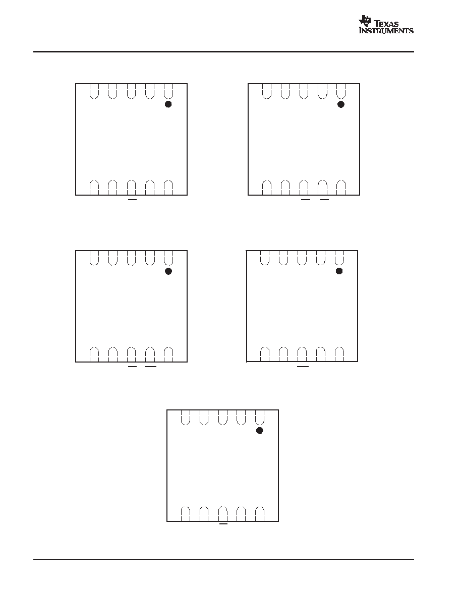
DRC PACKAGE
(TOP VIEW)
VSS
5
STAT2
4
STAT1
3
USB
2
AC
1
6
7
8
9
10
ISET1
CE
TS
OUT
bq24020DRC
bq24025DRC
DRC PACKAGE
(TOP VIEW)
VSS
5
STAT2
4
STAT1
3
USB
2
AC
1
6
7
8
9
10
ISET1
PG
CE
ISET2
OUT
bq24022DRC
DRC PACKAGE
(TOP VIEW)
VSS
5
STAT2
4
STAT1
3
USB
2
AC
1
6
7
8
9
10
ISET1
CE
TTE
OUT
bq24023DRC
ISET2
ISET2
DRC PACKAGE
(TOP VIEW)
VSS
5
STAT2
4
STAT1
3
USB
2
AC
1
6
7
8
9
10
ISET1
TTE
TS
OUT
bq24024DRC
ISET2
DRC PACKAGE
(TOP VIEW)
VSS
5
STAT2
4
STAT1
3
USB
2
AC
1
6
7
8
9
10
ISET1
TE
TS
OUT
bq24026DRC
ISET2
bq24020, bq24022,
bq24023, bq24024
bq24025, bq24026
SLUS549C - DECEMBER 2002 - REVISED AUGUST 2004
www.ti.com
7
TERMINAL FUNCTIONS
TERMINAL
NAME
bq24020
bq24025
bq24022
bq24023
bq24024
bq24026
I/O
DESCRIPTION
AC
1
1
1
1
1
I
AC charge input voltage
CE
8
9
8
-
-
I
Charge enable input (active low)
ISET1
6
6
6
6
6
I
Charge current set point for AC input and precharge and taper set
point for both AC and USB
ISET2
7
7
7
7
7
I
Charge current set point for USB port (high=500 mA, Low=100
mA, hi-z=disable USB charge)
OUT
10
10
10
10
10
O
Charge current output
PG
-
8
-
-
-
O
Powergood status output (active low)
STAT1
3
3
3
3
3
O
Charge status output 1 (open-drain)
STAT2
4
4
4
4
4
O
Charge status output 2 (open-drain)
TE
-
-
-
-
8
I
Timer enable input (active low)
TS
9
-
-
9
9
I
Temperature sense input
TTE
-
-
9
8
-
I
Timer and termination enable input (active low)
USB
2
2
2
2
2
I
USB charge input voltage
VSS
5
5
5
5
5
-
Ground input
Exposed
Thermal
Pad
pad
pad
pad
pad
pad
-
There is an internal electrical connection between the exposed
thermal pad and VSS pin of the device. The exposed thermal pad
must be connected to the same potential as the Vss pin on the
printed circuit board. Do not use the thermal pad as the primary
ground input for the device. VSS pin must be connected to
ground at all times

bq24020, bq24022,
bq24023, bq24024
bq24025, bq24026
SLUS549C - DECEMBER 2002 - REVISED AUGUST 2004
www.ti.com
8
FUNCTIONAL BLOCK DIAGRAM
AC
USB
+
+
OUT
ISET1
REF
BIAS
AND
UVLO
ISET2
CHARGE
CONTROL,
TIMER,
AND
DISPLAY
LOGIC
THERMAL
SHUTDOWN
PRECHARGE
RECHARGE
TAPER
CHG ENABLE
STAT1
STAT2
TERM
CHG
ENABLE
CE
USB
AC
SUSPEND
SLEEP (AC)
SLEEP (USB)
VO(REG)
VSS
TS
500 mA/ 100 mA
USB CHARGE
500 mA/ 100 mA
PRECHARGE
(C/10)
ISET1
*
*
*
*
*
*
*
*
*
SIGNAL DEGLITCHED
I(TS)
V(HTF)
V(LTF)
t(TAPER) TIMER
VI(OUT)
VI(AC)
VI(OUT)
VI(USB)
VI(OUT)
VI(OUT)
VI(SET)
VI(SET)
VI(SET)
AC/USB
VI(ISET-USB)
VI(SET)
VI(OUT)
VI(REG)
VI(AC)
VI(USB)
VI(OUT)
VI(ISET)
VI(ISET-USB)
AC/USB
V(SET)
AC/USB
sensefet
sensefet
sensefet
100 mA/500 mA
VBAT
UDG-02185
TTE
OR
TE
PG
VO(REG)
UVLO
bq24020, bq24022,
bq24023, bq24024
bq24025, bq24026
SLUS549C - DECEMBER 2002 - REVISED AUGUST 2004
www.ti.com
9
TYPICAL CHARACTERISTICS
0
100
0
50
150
50
300
200
350
250
400
450
100
150
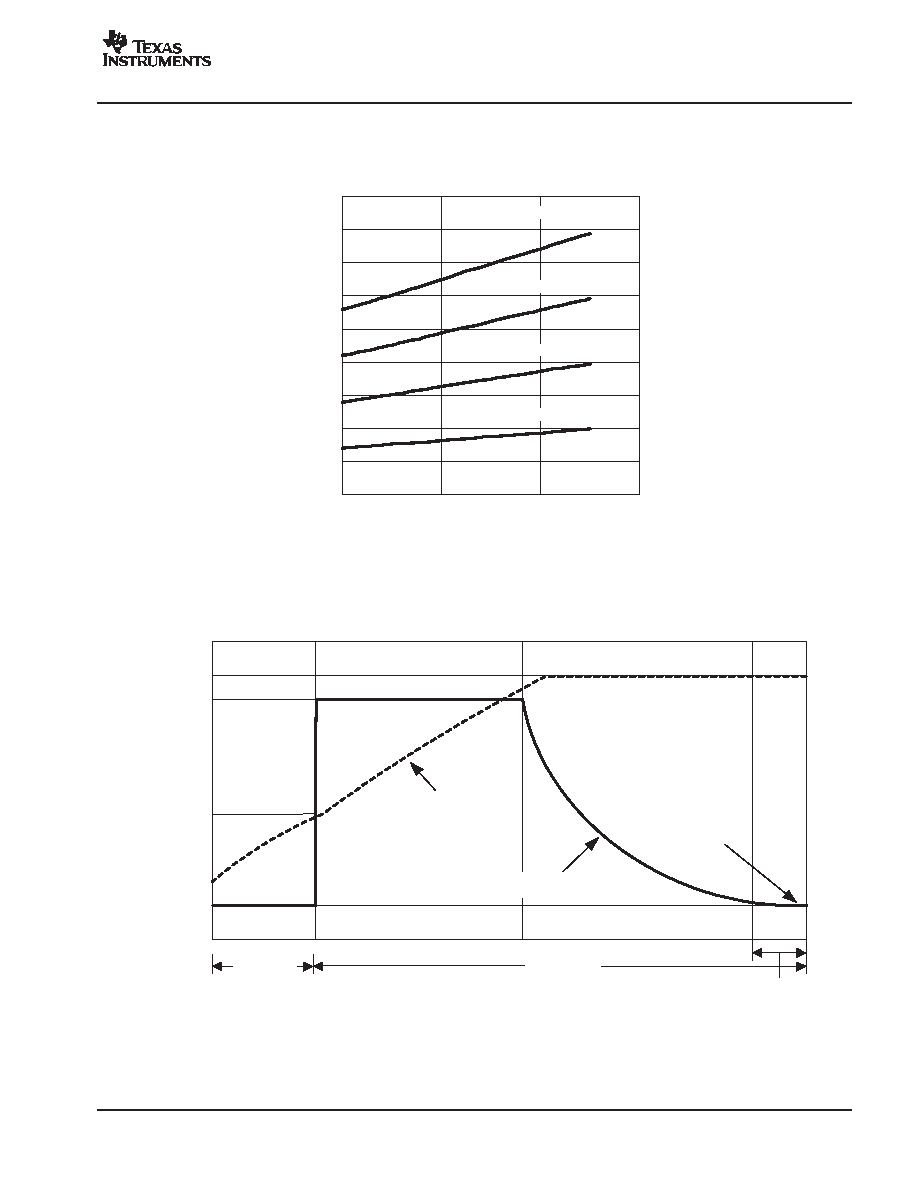
Figure 1
IO(OUT) = 1000 mA
AC DROPOUT VOLTAGE
vs
JUNCTION TEMPERATURE
TJ - Junction Temperature -
_
C
Dropout V
oltage - mV
IO(OUT) = 750 mA
IO(OUT) = 500 mA
IO(OUT) = 250 mA
The bqTINYII supports a precision Li-Ion, Li-Pol charging system suitable for single-cells. Figure 3 shows a typical charge
profile, application circuit and Figure 4 shows an operational flow chart.
Regulation
Voltage
Regulation
Current
Minimum
Charge
Voltage
Pre-Conditioning
and Taper Detect
t(PRECHG)
t(CHG)
t(TAPER)
Charge
Voltage
Charge
Current
Charge
Complete
Pre-Conditioning
Phase
Current Regulation
Phase
Voltage Regulation
and Charge Termination Phase
Figure 2. Typical Charging Profile
bq24020, bq24022,
bq24023, bq24024
bq24025, bq24026
SLUS549C - DECEMBER 2002 - REVISED AUGUST 2004
www.ti.com
10
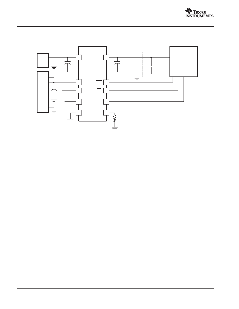
FUNCTIONAL DESCRIPTION
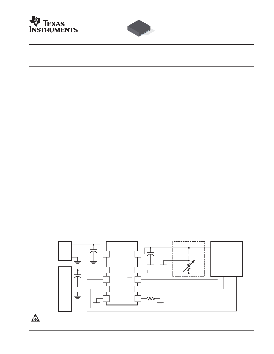
UDG-02184
RSET
1
2
3
4
10
9
8
5
AC
USB
OUT
VSS
STAT1
STAT2
7
6
ISET2
ISET1
bq24023DRC
PACK+
PACK-
SYSTEM
SYSTEM
INTERFACE
VDC
GND
VBUS
GND
D+
D -
USB PORT
AC ADAPTER
+
TTE
CE
0.1
µ
F
Figure 3. Typical Application Circuit
bq24020, bq24022,
bq24023, bq24024
bq24025, bq24026
SLUS549C - DECEMBER 2002 - REVISED AUGUST 2004
www.ti.com
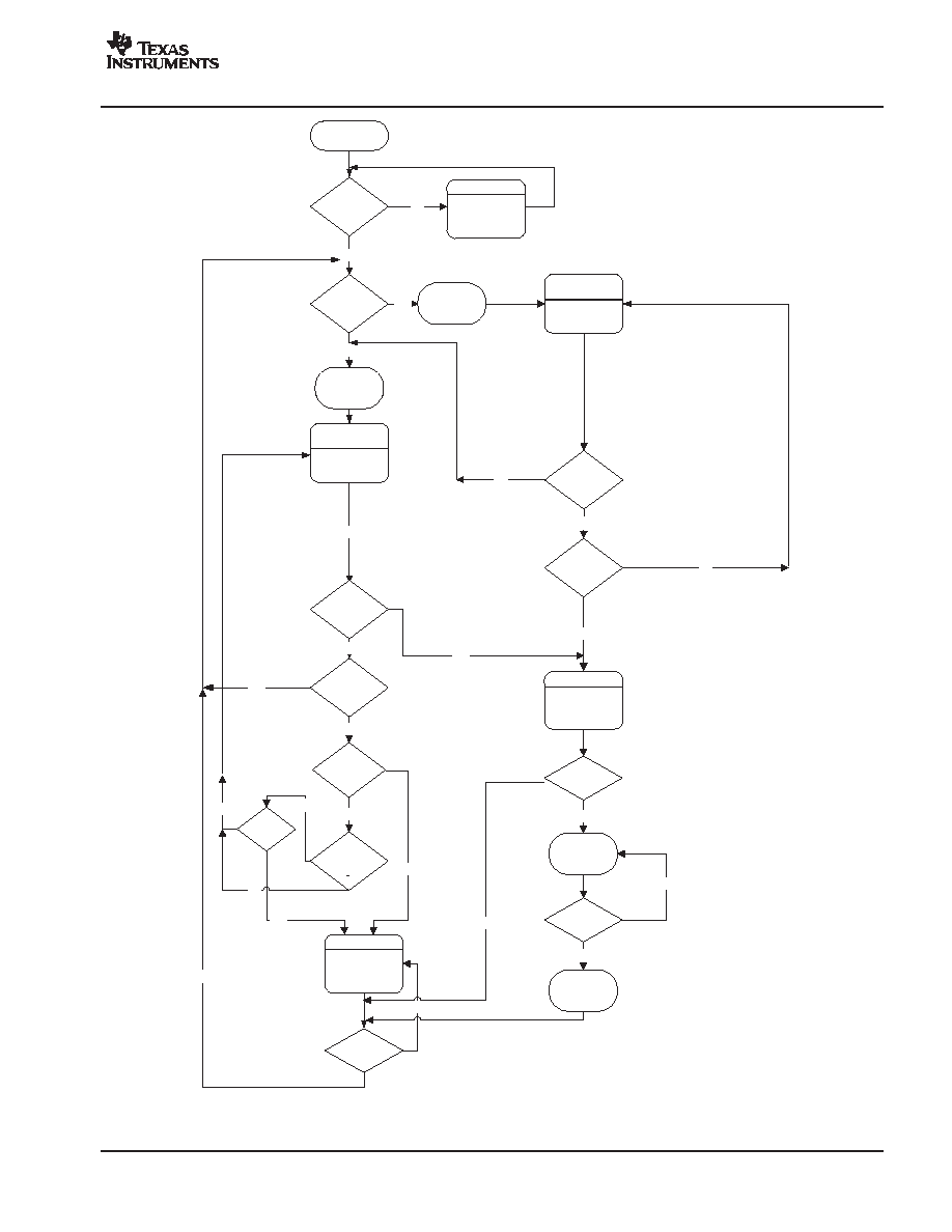
11
Vcc > V
I(OUT)
checked at all times
V
I(OUT)
<V
(LOWV)
Yes
No
t
(PRECHG)
Expired?
No
Yes
Indicate Fault
Yes
No
Yes
t
(CHG)
Expired?
No
Indicate Charge-
In-Progress
Regulate
I
O(PRECHG)
Indicate Charge-
In-Progress
Regulate Current
or Voltage
No
Reset and Start
t
(PRECHG)
timer
POR
Yes
Reset all timers,
Start t
(CHG)
timer
I
(TERM)
detection?
No
Yes
V
I(OUT)
< V
(RCH)
?
No
V
I(OUT)
<V
(LOWV)
No
Fault Condition
Yes
Yes
Indicate DONE
Turn off charge
Indicate SLEEP
MODE
SLEEP MODE
V
I(OUT)
<V
(LOWV)
I
(TAPER)
detection?
t
(TAPER)
Expired?
No
No
Yes
Yes
No
Yes
V
I(OUT)
> V
(RCH)
?
Enable I
(FAULT)
current
V
I(OUT)
> V
(RCH)
?
No
Yes
Yes
Disable I
(FAULT)
current
(1) t(TAPER) does not apply to bq24026
(1)
Figure 4. Operational Flow Chart

bq24020, bq24022,
bq24023, bq24024
bq24025, bq24026
SLUS549C - DECEMBER 2002 - REVISED AUGUST 2004
www.ti.com
12
FUNCTIONAL DESCRIPTION
AUTONOMOUS POWER SOURCE SELECTION
As default the bqTINY-II attempts to charge from the AC input. If AC input is not present, the USB is selected. If both inputs
are available, the AC adapter has the priority. See Figure 5 for details.
UDG-02187
USB MODE
AC MODE
AC > BATTERY
AC < BATTERY
USB > BATTERY
Figure 5. Typical Charging Profile
TEMPERATURE QUALIFICATION (bq24020, bq24024, bq24025, and bq24026 only)
The bqTINY-II continuously monitors battery temperature by measuring the voltage between the TS and VSS pins.
An internal current source provides the bias for most common 10-k
negative-temperature coefficient thermistors
(NTC) (see Figure 6). The device compares the voltage on the TS pin against the internal V
(LTF)
and V
(HTF)
thresholds
to determine if charging is allowed. Once a temperature outside the V
(LTF)
and V
(HTF)
thresholds is detected the
device immediately suspend the charge. The device suspend charge by turning off the powerFET and holding the
timer value (i.e. timers are NOT reset). Charge is resumed when the temperature returns to the normal range.
The allowed temperature range for 103AT type thermistor is 0
_
C to 45
_
C. However the user may modify these
thresholds by adding two external resistors. See Figure 7.
BATTERY PRE-CONDITIONING
During a charge cycle if the battery voltage is below the V
(LOWV)
threshold, the bqTINY-II applies a precharge current,
I
o(PRECHG)
, to the battery. This feature revives deeply discharged cells. The resistor connected between the ISET1
and Vss, R
SET
, determines the precharge rate. The V
(PRECHG)
and K
(SET)
parameters are specified in the
specifications table. Note that this applies to both AC and USB charging.
I
O (PRECHG)
+
V
(PRECGH)
K
(SET)
R
SET
The bqTINY-II activates a safety timer, t
(PRECHG)
, during the conditioning phase. If V
(LOWV)
threshold is not reached
within the timer period, the bqTINY-II turns off the charger and enunciates FAULT on the STATx pins. Please refer
to the TIMER FAULT RECOVERY section for additional details.
Figure 6. Temperature Sensing Configuration
9
TS
bqTINYII
LTF
HTF
+
BATTERY
PACK
PACK+
PACK-
NTC
VLTF
VHTF
ITS
TEMP
UDG-02186
Figure 7. Temperature Sensing Thresholds
VLTF
VHTF
ITS
9
TS
bqTINYII
LTF
HTF
+
BATTERY
PACK
PACK+
PACK-
NTC
RT1
RT2
TEMP
UDG-02188
(1)

bq24020, bq24022,
bq24023, bq24024
bq24025, bq24026
SLUS549C - DECEMBER 2002 - REVISED AUGUST 2004
www.ti.com
13
FUNCTIONAL DESCRIPTION
BATTERY CHARGE CURRENT
The bqTINY-II offers on-chip current regulation with programmable set point. The resistor connected between the
ISET1 and V
SS
, R
SET
, determines the AC charge rate. The V
(SET)
and K
(SET)
parameters are specified in the
specifications table.
I
O (OUT)
+
V
(SET)
K
(SET)
R
SET
When charging from a USB port, the host controller has the option of selecting either 100 mA or 500 mA charge rate
using ISET2 pin. A low-level signal sets current at 100 mA and a high level signal sets current at 500 mA. A high-Z
input disables USB charging
BATTERY VOLTAGE REGULATION
The voltage regulation feedback is through the OUT pin. This input is tied directly to the positive side of the battery
pack. The bqTINY-II monitors the battery-pack voltage between the OUT and VSS pins. When the battery voltage
rises to V
O(REG)
threshold, the voltage regulation phase begins and the charging current begins to taper down.
As a safety backup, the bqTINY-II also monitors the charge time in the charge mode. If charge is not terminated within
this time period, t
(CHG)
, the bqTINY-II turns off the charger and enunciates FAULT on the STATx pins. Please refer
to the TIMER FAULT RECOVERY section for additional details.
CHARGE TAPER DETECTION, TERMINATION AND RECHARGE
The bqTINY-II monitors the charging current during the voltage regulation phase. Once the taper threshold, I
(TAPER)
,
is detected the bqTINY-II initiates the taper timer, t
(TAPER)
. Charge is terminated after the timer expires. The resistor
connected between the ISET1 and V
SS
, R
SET
, determines the taper detection level. The V
(TAPER)
and K
(SET)
parameters are specified in the specifications table. Note that this applies to both AC and USB charging.
I
(TAPER)
+
V
(TAPER)
K
(SET)
R
SET
The bqTINY-II resets the taper timer in the event that the charge current returns above the taper threshold, I
(TAPER)
.
In addition to the taper current detection, the bqTINY-II terminates charge in the event that the charge current falls
below the I
(TERM)
threshold. This feature allows for quick recognition of a battery removal condition or insertion of
a fully charged battery. Note that charge timer and taper timer are bypassed for this feature. The resistor connected
between the ISET1 and V
SS
, R
SET
, determines the taper detection level. The V
(TERM)
and K
(SET)
parameters are
specified in the specifications table. Note that this applies to both AC and USB charging.
I
(TERM)
+
V
(TERM)
K
(SET)
R
SET
After charge termination, the bqTINY-II re-starts the charge once the voltage on the OUT pin falls below the V
(RCH)
threshold. This feature keeps the battery at full capacity at all times.
NOTE ON bq24026
The bq24026 monitors the charging current during the voltage regulation phase. Once the taper threshold, I
(TAPER)
,
is detected the bq24026 terminates the charge. There is no taper timer, t
(TAPER)
for this version.
The resistor connected between the ISET1 and V
SS
, R
SET
, determines the taper detection level for AC input. For USB
charge, taper level is fixed at 10% of the 100- or 500-mA charge rate.
Also note that there is I
(TERM)
detection in bq24026.
(2)
(3)
(4)

bq24020, bq24022,
bq24023, bq24024
bq24025, bq24026
SLUS549C - DECEMBER 2002 - REVISED AUGUST 2004
www.ti.com
14
FUNCTIONAL DESCRIPTION
SLEEP MODE
The bqTINY-II enters the low-power sleep mode if both AC and USB are removed from the circuit. This feature
prevents draining the battery during the absence of input supply.
CHARGE STATUS OUTPUTS
The open-drain STAT1 and STAT2 outputs indicate various charger operations as shown in the following table. These
status pins can be used to drive LEDs or communicate to the host processor. Note that OFF indicates the open-drain
transistor is turned off.
Table 1. Status Pins Summary
CHARGE STATE
STAT1
STAT2
Precharge in progress
ON
ON
Fast charge in progress
ON
OFF
Charge done
OFF
ON
Charge suspend (temperature)
OFF
OFF
Timer fault
OFF
OFF
Sleep mode
OFF
OFF
(
{
)
OFF means the open-drain output transistor on the STAT1 and
STAT2 pins is in an off state.
PG OUTPUT
The open-drain PG (Power Good) indicates when the AC adapter is present. The output turns ON when a valid
voltage is detected. This output is turned off in the sleep mode. The PG pin can be used to drive an LED or
communicate to the host processor.
CE INPUT (CHARGE ENABLE)
The CE digital input is used to disable or enable the charge process. A low-level signal on this pin enables the charge
and a high-level signal disables the charge and places the device in a low-power mode. A high-to-low transition on
this pin also resets all timers and timer fault conditions. Note that this applies to both AC and USB charging.
TTE INPUT (TIMER AND TERMINATION ENABLE)
The TTE digital input is used to disable or enable the fast-charge timer and charge taper detection. A low-level signal
on this pin enables the fast-charge timer and taper timer and a high-level signal disables this feature. Note that this
applies to both AC and USB charging.
THERMAL SHUTDOWN AND PROTECTION
The bqTINY-II monitors the junction temperature, T
J
, of the die and suspends charging if T
J
exceeds T
(SHTDWN)
.
Charging resumes when T
J
falls below T
(SHTDWN)
by approximately 15
_
C.
TE INPUT (TIMER ENABLED)
The TE digital input is used to disable or enable the fast-charge timer. A low-level signal on this pin enables the
fast-charge timer and a high-level signal disables this feature.
Note that this applies to both AC and USB charging.

bq24020, bq24022,
bq24023, bq24024
bq24025, bq24026
SLUS549C - DECEMBER 2002 - REVISED AUGUST 2004
www.ti.com
15
FUNCTIONAL DESCRIPTION
TIMER FAULT RECOVERY
As shown in Figure 4, bqTINY-II provides a recovery method to deal with timer fault conditions. The following
summarizes this method:
Condition #1: Charge voltage above recharge threshold (V
(RCH)
) and timeout fault occurs
Recovery method: bqTINY-II waits for the battery voltage to fall below the recharge threshold. This could happen
as a result of a load on the battery, self-discharge or battery removal. Once the battery falls below the recharge
threshold, the bqTINY-II clears the fault and starts a new charge cycle. A POR or CE or TTE toggle also clears the
fault.
Condition #2: Charge voltage below recharge threshold (V
(RCH)
) and timeout fault occurs
Recovery method: Under this scenario, the bqTINY-II applies the I
(FAULT)
current. This small current is used to detect
a battery removal condition and remains on as long as the battery voltage stays below the recharge threshold. If the
battery voltage goes above the recharge threshold, then the bqTINY-II disables the I
(FAULT)
current and executes the
recovery method described for condition #1. Once the battery falls below the recharge threshold, the bqTINY-II clears
the fault and starts a new charge cycle. A POR or CE or TTE toggle also clears the fault.

bq24020, bq24022,
bq24023, bq24024
bq24025, bq24026
SLUS549C - DECEMBER 2002 - REVISED AUGUST 2004
www.ti.com
16
APPLICATION INFORMATION
THERMAL CONSIDERATIONS
The bqTINY-II is packaged in a thermally enhanced MLP package. The package includes a thermal pad to provide
an effective thermal contact between the device and the printed circuit board (PCB). Full PCB design guidelines for
this package are provided in the application note entitled, QFN/SON PCB Attachment Application Note (TI Literature
No. SLUA271).
The most common measure of package thermal performance is thermal impedance (
JA
) measured (or modeled)
from the device junction to the air surrounding the package surface (ambient). The mathematical expression for
JA
is:
q
JA
+
T
J
*
T
A
P
Where:
D
T
J
= device junction temperature
D
T
A
= ambient temperature
D
P = device power dissipation
Factors that can greatly influence the measurement and calculation of
JA
include:
D
whether or not the device is board mounted
D
trace size, composition, thickness, and geometry
D
orientation of the device (horizontal or vertical)
D
volume of the ambient air surrounding the device under test and airflow
D
whether other surfaces are in close proximity to the device being tested
The device power dissipation, P, is a function of the charge rate and the voltage drop across the internal PowerFET.
It can be calculated from the following equation:
P
+
V
IN
*
V
I(BAT)
I
O(OUT)
Due to the charge profile of Li-xx batteries, the maximum power dissipation is typically seen at the beginning of the
charge cycle when the battery voltage is at it's lowest. See Figure 2.
PCB LAYOUT CONSIDERATIONS
It is important to pay special attention to the PCB layout. The following provides some guidelines:
D
To obtain optimal performance, the decoupling capacitor from V
CC
to V
SS
and the output filter capacitors from
OUT to VSS should be placed as close as possible to the bqTINY, with short trace runs to both signal and V
SS
pins.
D
All low-current V
SS
connections should be kept separate from the high-current charge or discharge paths from
the battery. Use a single-point ground technique incorporating both the small signal ground path and the power
ground path.
D
The BAT pin is the voltage feedback to the device and should be connected with its trace as close to the battery
pack as possible.
D
The high current charge paths into IN and from the OUT pins must be sized appropriately for the maximum charge
current in order to avoid voltage drops in these traces.
D
The bqTINY-II is packaged in a thermally enhanced MLP package. The package includes a thermal pad to
provide an effective thermal contact between the device and the printed circuit board (PCB). Full PCB design
guidelines for this package are provided in the application note entitled: QFN/SON PCB Attachment Application
Note (TI Literature No. SLUA271).
(5)
(6)

bq24020, bq24022,
bq24023, bq24024
bq24025, bq24026
SLUS549C - DECEMBER 2002 - REVISED AUGUST 2004
www.ti.com
17
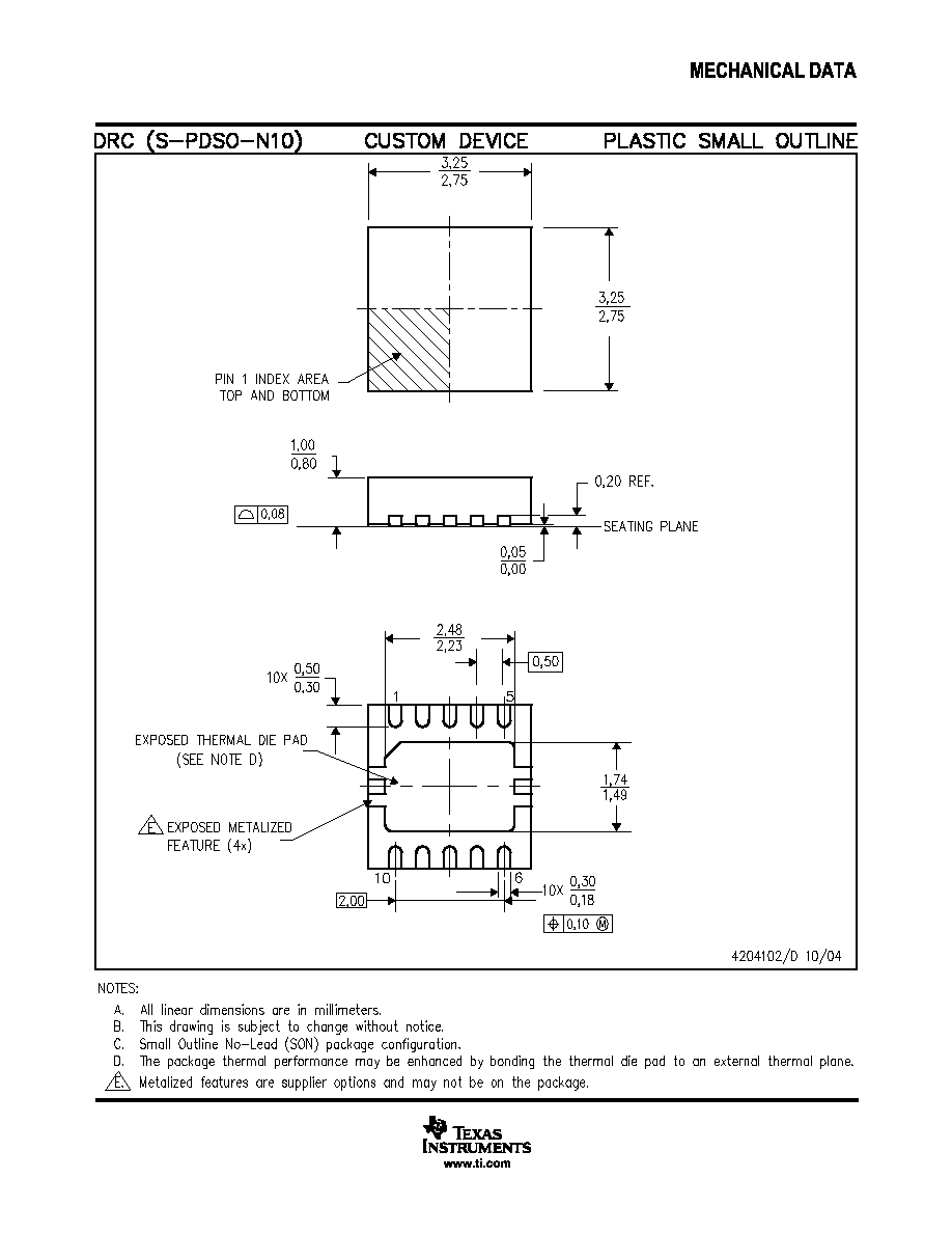
DRC (S-PDSO-N10) CUSTOM DEVICE PLASTIC SMALL OUTLINE
4204102/B 04/02
SEATING PLANE
0,20 REF.
1,00
0,80
10
0,18
0,30
10
0,50
0,30
0,50
0,05
(SEE NOTE D)
EXPOSED THERMAL DIE PAD
TOP AND BOTTOM
PIN 1 INDEX AREA
3,25
3,25
0,00
1
2,23
2,75
2,75
5
10
6
2,00
1,74
2,48
1,49
0,10
0,08
NOTES:A. All linear dimensions are in millimeters.
B. This drawing is subject to change without notice.
C. Small Outline No-Lead (SON) package configuration.
D. The package thermal performance may be enhanced by bonding the thermal die pad to an external thermal plane.

IMPORTANT NOTICE
Texas Instruments Incorporated and its subsidiaries (TI) reserve the right to make corrections, modifications,
enhancements, improvements, and other changes to its products and services at any time and to discontinue
any product or service without notice. Customers should obtain the latest relevant information before placing
orders and should verify that such information is current and complete. All products are sold subject to TI's terms
and conditions of sale supplied at the time of order acknowledgment.
TI warrants performance of its hardware products to the specifications applicable at the time of sale in
accordance with TI's standard warranty. Testing and other quality control techniques are used to the extent TI
deems necessary to support this warranty. Except where mandated by government requirements, testing of all
parameters of each product is not necessarily performed.
TI assumes no liability for applications assistance or customer product design. Customers are responsible for
their products and applications using TI components. To minimize the risks associated with customer products
and applications, customers should provide adequate design and operating safeguards.
TI does not warrant or represent that any license, either express or implied, is granted under any TI patent right,
copyright, mask work right, or other TI intellectual property right relating to any combination, machine, or process
in which TI products or services are used. Information published by TI regarding third-party products or services
does not constitute a license from TI to use such products or services or a warranty or endorsement thereof.
Use of such information may require a license from a third party under the patents or other intellectual property
of the third party, or a license from TI under the patents or other intellectual property of TI.
Reproduction of information in TI data books or data sheets is permissible only if reproduction is without
alteration and is accompanied by all associated warranties, conditions, limitations, and notices. Reproduction
of this information with alteration is an unfair and deceptive business practice. TI is not responsible or liable for
such altered documentation.
Resale of TI products or services with statements different from or beyond the parameters stated by TI for that
product or service voids all express and any implied warranties for the associated TI product or service and
is an unfair and deceptive business practice. TI is not responsible or liable for any such statements.
Following are URLs where you can obtain information on other Texas Instruments products and application
solutions:
Products
Applications
Amplifiers
amplifier.ti.com
Audio
www.ti.com/audio
Data Converters
dataconverter.ti.com
Automotive
www.ti.com/automotive
DSP
dsp.ti.com
Broadband
www.ti.com/broadband
Interface
interface.ti.com
Digital Control
www.ti.com/digitalcontrol
Logic
logic.ti.com
Military
www.ti.com/military
Power Mgmt
power.ti.com
Optical Networking
www.ti.com/opticalnetwork
Microcontrollers
microcontroller.ti.com
Security
www.ti.com/security
Telephony
www.ti.com/telephony
Video & Imaging
www.ti.com/video
Wireless
www.ti.com/wireless
Mailing Address:
Texas Instruments
Post Office Box 655303 Dallas, Texas 75265
Copyright
2004, Texas Instruments Incorporated