 | –≠–ª–µ–∫—Ç—Ä–æ–Ω–Ω—ã–π –∫–æ–º–ø–æ–Ω–µ–Ω—Ç: BQ24038 | –°–∫–∞—á–∞—Ç—å:  PDF PDF  ZIP ZIP |
www.ti.com
FEATURES
APPLICATIONS
DESCRIPTION
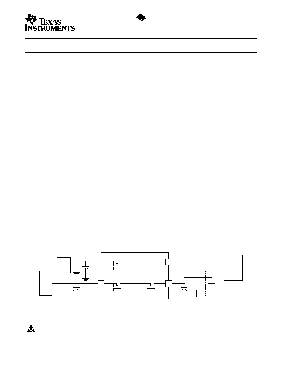
AC
USB
BAT
OUT
bq2403x
PACK+
PACK-
System
VDC
GND
VBUS
GND
D+
D -
USB Port
AC Adapter
+
Q1
Q2
Q3
UDG-04082
40 m
(2)
bq24030, bq24031, bq24032,
bq24032A, bq24035, bq24038, bq24039
SLUS618C ≠ AUGUST 2004 ≠ REVISED JUNE 2005
SINGLE-CHIP CHARGE AND SYSTEM POWER-PATH MANAGEMENT IC (bqTINYTM-III)
∑
Smart Phones and PDA
∑
Small 3,5 mm ◊ 4,5 mm QFN Package
∑
MP3 Players
∑
Designed for Single-Cell Li-Ion- or
∑
Digital Cameras Handheld Devices
Li-Polymer-Based Portable Applications
∑
Internet Appliances
∑
Integrated Dynamic Power-Path Management
(DPPM) Feature Allowing the AC Adapter or
the USB Port to Simultaneously Power the
System and Charge the Battery
The bqTINYTM-III series of devices are highly inte-
∑
Power Supplement Mode Allows Battery to
grated Li-ion linear chargers and system power-path
management devices targeted at space-limited port-
Supplement the USB or AC Input Current
able applications. The bqTINY-III series offer inte-
∑
Autonomous Power Source Selection (AC
grated USB-port and DC supply (AC adapter),
Adapter or USB)
power-path
management
with
autonomous
∑
Integrated USB Charge Control With
power-source selection, power FETs and current
Selectable 100-mA and 500-mA Maximum
sensors, high accuracy current and voltage regu-
Input Current Regulation Limits
lation, charge status, and charge termination, in a
single monolithic device.
∑
USB High Current Regulation Limit, 1 A Max
(bq24039 Only)
The bqTINY-III powers the system while indepen-
dently charging the battery. This feature reduces the
∑
Dynamic Total Current Management
charge and discharge cycles on the battery, allows
for USB
for proper charge termination and allows the system
∑
Supports Up to 2-A Total Current
to run with an absent or defective battery pack. This
∑
3.3-V Integrated LDO Output
feature also allows for the system to instantaneously
turn on from an external power source in the case of
∑
Thermal Regulation for Charge Control
a deeply discharged battery pack. The IC design is
∑
Charge Status Outputs for LED or System
focused on supplying continuous power to the system
Interface Indicates Charge and Fault
when available from the AC, USB, or battery sources.
Conditions
∑
Reverse Current, Short-Circuit, and Thermal
Protection
∑
Power Good (AC Adapter and USB Port
Present) Status Outputs
∑
Charge Voltage Options: 4.2 V or 4.36 V
POWER FLOW DIAGRAM
(1)
(1)
See Figure 2 and functional block diagram for more detailed feature information.
(2)
P-FET back gate body diodes are disconnected to prevent body diode conduction.
Please be aware that an important notice concerning availability, standard warranty, and use in critical applications of Texas
Instruments semiconductor products and disclaimers thereto appears at the end of this data sheet.
bqTINY is a trademark of Texas Instruments.
UNLESS OTHERWISE NOTED this document contains PRO-
Copyright © 2004≠2005, Texas Instruments Incorporated
DUCTION DATA information current as of publication date. Prod-
ucts conform to specifications per the terms of Texas Instruments
standard warranty. Production processing does not necessarily
include testing of all parameters.

www.ti.com
DESCRIPTION (CONTINUED)
bq24030, bq24031, bq24032,
bq24032A, bq24035, bq24038, bq24039
SLUS618C ≠ AUGUST 2004 ≠ REVISED JUNE 2005
These devices have limited built-in ESD protection. The leads should be shorted together or the device
placed in conductive foam during storage or handling to prevent electrostatic damage to the MOSFET
gates.
The power select pin, PSEL, defines which input source is to be used first (primary source ≠ AC or USB). If the
primary source is not available, then the IC automatically switches over to the other secondary source if available
or the battery as the last option. If the PSEL is set low, the USB input is selected first and if not available, the AC
line is selected (if available) but programmed to a USB input limiting rate (100 mA/500 mA max). This feature
allows the use of one input connector, where the host programs the PSEL pin according to what source is
connected (AC adaptor or USB port).
The bq24039 has replaced the PSEL pin (node now tied high internally ≠ AC priority) with the ISET3 pin that
allows for twice the standard USB input limiting current levels (200 mA/1000 mA), when set to high. This is a
feature for manufacturers that supply their own USB power source that is rated for this higher current level.
The bq24038 replaces USBPG with pin VBSEL, to enable user selection of the charge voltage. In addition, pin
ACPG was modified to PG. PG is active low when either ac power or USB power is detected.
The ISET1 pin programs the battery's fast charge constant current level with a resistor. During normal AC
operation, the input supply provides power to both the OUT (System) and BAT pins. For peak or excessive loads
(typically when operating from the USB power, PSEL = Low) that would cause the input source to enter current
limit (or Q3 - USB FET limiting current) and its source and system voltage (OUT pin) to drop, the dynamic
power-path management (DPPM) feature reduces the charging current attempting to prevent any further drop in
system voltage. This feature allows the selection of a lower current rated adaptor based on the average load
(I
SYS-AVG
+ I
BAT-PGM
) rather than a high peak transient load.
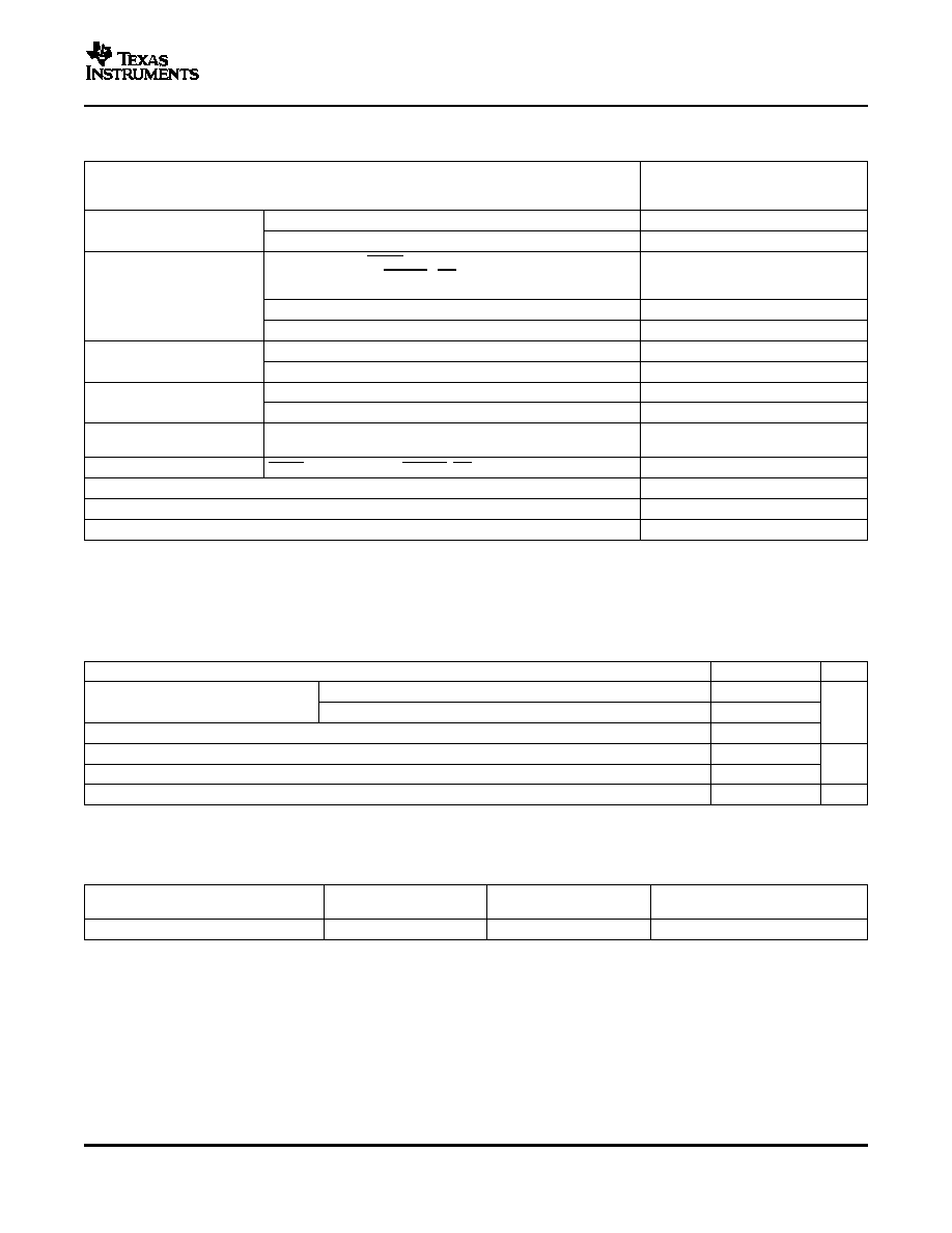
ORDERING INFORMATION
(1)
BATTERY
OUT PIN FOR AC
PART
PACKAGE
T
A
STATUS
VOLTAGE (V)
INPUT CONDITIONS
NUMBER
(2) (3)
MARKING
4.2
Regulated to 6 V
(4)
bq24030RHLR
Released
ANB
4.2
Regulated to 4.4 V
(4)
bq24032RHLR
Released
AMZ
≠40∞C to 125∞C
4.2
Regulated to 4.4 V
(4)
bq24032ARHLR
Released
BPE
4.2
Regulated to 4.4 V
(4)
bq24032ARHLT
Released
BPE
4.2
Cutoff for AC overvoltage
(5)
bq24035RHLR
Released
ANA
4.2
Cutoff for AC overvoltage
(5)
bq24039RHLR
Preview
ANH
4.36
Regulated to 6 V
(4)
bq24031RHLR
Preview
BOU
4.36
Regulated to 6 V
(4)
bq24031RHLT
Preview
BOU
4.2/4.36 Selectable
Regulated to 4.4 V
bq24038RHLR
Released
BOW
4.2/4.36 Selectable
Regulated to 4.4 V
bq24038RHLT
Released
BOW
(1)
For the most current package and ordering information, see the Package Option Addendum at the end of this document, or see the TI
Web site at
www.ti.com.
(2)
The RHL package is available in the following options:
R - taped and reeled in quantities of 3,000 devices per reel.
T - taped and reeled in quantities of 250 devices per reel.
(3)
This product is RoHS compatible, including a lead concentration that does not exceed 0.1% of total product weight, and is suitable for
use in specified lead-free soldering processes. In addition, this product uses package materials that do not contain halogens, including
bromine (Br) or antimony (Sb) above 0.1% of total product weight.
(4)
If AC < V
O(OUT-REG)
, the AC is connected to the OUT pin by a P-FET, (Q1).
(5)
If AC > V
(CUT-OFF)
the P-FET disconnects the OUT pin from the AC.
2
www.ti.com
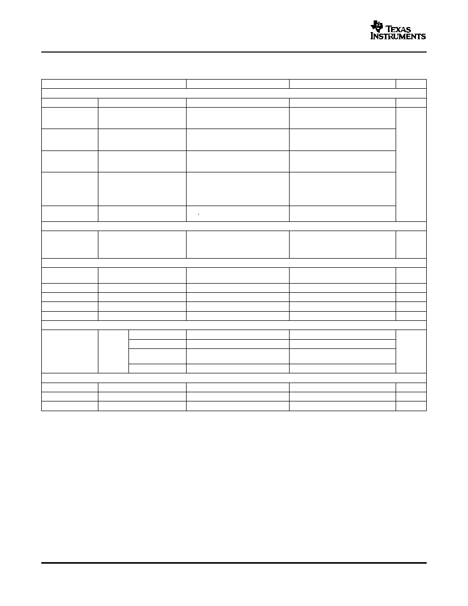
ABSOLUTE MAXIMUM RATINGS
(1)
RECOMMENDED OPERATING CONDITIONS
DISSIPATION RATINGS
bq24030, bq24031, bq24032,
bq24032A, bq24035, bq24038, bq24039
SLUS618C ≠ AUGUST 2004 ≠ REVISED JUNE 2005
over operating free-air temperature range (unless otherwise noted)
bq24030, bq24031,
bq24032, bq24032A,
bq24035, bq24038. bq24039
AC (DC voltage wrt (with respect to) VSS)
≠0.3 V to 18 V
Input voltage
USB (DC voltage wrt VSS)
≠0.3 V to 7 V
BAT, CE, DPPM, ACPG, PSEL, OUT, ISET1, ISET2, ISET3,
STAT1, STAT2, TS, USBPG , PG, VBSEL (all DC voltages wrt
≠0.3 V to 7 V
VSS)
Input voltage
LDO (DC voltage wrt VSS)
≠0.3 V to V
O(OUT)
+ 0.3 V
TMR
≠0.3 V to V
O(LDO)
+ 0.3 V
AC
3.5 A
Input current
USB
1000 mA
OUT
4 A
Output current
BAT
(2)
≠4 A to 3.5 A
Output source current (in
LDO
30 mA
regulation at 3.3 V LDO)
Output sink current
ACPG, STAT1, STAT2, USBPG, PG
1.5 mA
Storage temperature range, T
stg
≠65∞C to 150∞C
Junction temperature range, T
J
≠40∞C to 150∞C
Lead temperature (soldering, 10 seconds)
300∞C
(1)
Stresses beyond those listed under absolute maximum ratings may cause permanent damage to the device. These are stress ratings
only, and functional operation of the device at these or any other conditions beyond those indicated under recommended operating
conditions is not implied. Exposure to absolute-maximum-rated conditions for extended periods may affect device reliability. All voltage
values are with respect to the network ground terminal unless otherwise noted.
(2)
Negative current is defined as current flowing into the BAT pin.
MIN
MAX
UNIT
bq24030/2/2A/5/9, bq24038 (at VBSEL = LOW)
4.35
16.00
Supply voltage (from AC input)
V
CC
(1) (2)
bq24031, bq24038 (at VBSEL = HIGH)
4.55
16
V
V
CC
Supply voltage (from USB input)
(1)
4.35
6.0
I
AC
Input current, AC
2
A
I
USB
Input current, USB
0.5
T
J
Operating junction temperature range
≠40
125
∞C
(1)
V
CC
is defined as the greater of AC or USB input.
(2)
Verify that power dissipation and junction temperatures are within limits at maximum V
CC
.
T
A
40∞C
DERATING FACTOR
PACKAGE
JA
POWER RATING
T
A
> 40∞C
20-pin RHL
(1)
1.81 W
21 mW/∞C
46.87 ∞C/W
(1)
This data is based on using the JEDEC High-K board and the exposed die pad is connected to a Cu pad on the board. This is
connected to the ground plane by a 2◊3 via matrix.
3
www.ti.com
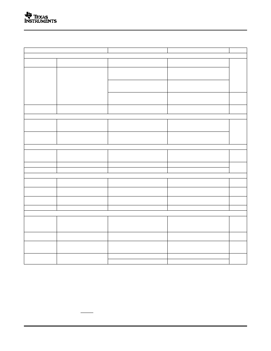
ELECTRICAL CHARACTERISTICS
bq24030, bq24031, bq24032,
bq24032A, bq24035, bq24038, bq24039
SLUS618C ≠ AUGUST 2004 ≠ REVISED JUNE 2005
over junction temperature range (0∞C
T
J
125∞C) and the recommended supply voltage range (unless otherwise noted)
PARAMETER
TEST CONDITIONS
MIN
TYP
MAX
UNIT
INPUT BIAS CURRENTS
I
CC(SPLY)
Active supply current, VCC
V
VCC
> V
VCC(min)
1
2
mA
V
(AC)
< V
(BAT)
, V
(USB)
< V
(BAT)
,
Sleep current (current into BAT
I
CC(SLP)
2.6 V
V
I(BAT)
V
O(BAT-REG)
,
2
5
pin)
Excludes load on OUT pin
V
I(AC)
6V, Total current into AC pin with
I
CC(AS-STDBY)
AC standby current
chip disabled, Excludes all loads,
200
CE=LOW, after t
(CE-HOLDOFF)
delay
Total current into USB pin with chip
I
CC(USB-STDBY)
USB standby current
disabled, Excludes all loads, CE=LOW,
200
µA
after t
(CE-HOLDOFF)
delay
Total current into BAT pin with AC and/or
USB present and chip disabled; Ex-
I
CC(BAT-STDBY)
BAT standby current
cludes all loads (OUT and LDO),
45
60
CE=LOW, after t
(CE-HOLDOFF)
delay,
0∞C
T
J
85∞C
(1)
Charge DONE, AC or USB supplying the
I
IB(BAT)
Charge done current, BAT
1
5
load
HIGH AC CUTOFF MODE
V
I(AC)
> 6.8 V, AC FET (Q1) turns off,
Input ac cutoff voltage
USB FET (Q3) turns on if USB power
V
CUT-OFF
6.1
6.4
6.8
V
(bq24039 is product preview)
present, otherwise BAT FET (Q2) turns
on.
LDO OUTPUT
Active only if AC or USB is present,
V
O(LDO)
Output regulation voltage
3.3
V
V
I(OUT)
V
O(LDO)
+ (I
O(LDO)
◊ R
DS(on)
)
Regulation accuracy
(2)
≠5%
5%
I
O(LDO)
Output current
20
mA
R
DS(on)
On resistance
OUT to LDO
50
C
(OUT)
(3)
Output capacitance
1
µF
OUT PIN-VOLTAGE REGULATION
bq24030/31
V
I(AC)
6 V+V
DO
6.0
6.3
bq24032/2A
V
I(AC)
4.4 V+V
DO
4.4
4.5
Output
V
O(OUT-REG)
regulation
V
VBSEL = HIGH or VBSEL = LOW,
bq24038
4.4
4.5
voltage
V
I(AC)
> 4.4 V+V
DO
bq24039
V
O(REG)
+ V
DD-AC
< V
AC
< V
CUT-OFF
6
6.3
OUT PIN ≠ DPPM REGULATION
V
(DPPM-SET)
DPPM set point
(4)
V
DPPM-SET
< V
OUT
2.6
5
V
I
(DPPM-SET)
DPPM current source
AC or USB present
95
100
105
µA
SF
DPPM scale factor
V
(DPPM-REG)
= V
(DPPM-SET)
◊ SF
1.139
1.150
1.162
(1)
This includes the quiescent current for the integrated LDO.
(2)
In standby mode (CE low) the accuracy is ±10%.
(3)
LDO output capacitor not required but one with a value of 0.1 µF is recommended.
(4)
V
(DPPM-SET)
is scaled up by the scale factor for controlling the output voltage V
(DPPM-REG)
.
4
www.ti.com
bq24030, bq24031, bq24032,
bq24032A, bq24035, bq24038, bq24039
SLUS618C ≠ AUGUST 2004 ≠ REVISED JUNE 2005
ELECTRICAL CHARACTERISTICS (continued)
over junction temperature range (0∞C
T
J
125∞C) and the recommended supply voltage range (unless otherwise noted)
PARAMETER
TEST CONDITIONS
MIN
TYP
MAX
UNIT
OUT PIN ≠ FET (Q1, Q3, AND Q2) DROP-OUT VOLTAGE (RDSon)
V
I(AC)
V
CC(min)
, PSEL=High,
V
(ACDO)
AC to OUT dropout voltage
(5)
300
475
I
I(AC)
= 1 A, (I
O(OUT)
+ I
O(BAT)
)
V
I(USB)
V
CC(min)
, PSEL = Low, or no AC
(bq24039), ISET2 = High
140
180
mV
I
I(USB)
= 0.4 A, (I
O(OUT)
+I
O(BAT)
)
V
I(USB)
V
CC(min)
, PSEL = Low, or no AC
V
(USBDO)
(6)
USB to OUT dropout voltage
(bq24039), ISET2 = Low
28
36
I
I(USB)
= 0.08 A, (I
O(OUT)
+ I
O(BAT)
)
V
I(USB)
V
CC(min)
, ISET2 = ISET3 = HIGH,
I
I(USB)
= 0.9 A (I
O(OUT)
+ I
O(BAT)
),
315
405
mV
bq24039 only
BAT to OUT dropout voltage
V
(BATDO)
V
I (BAT)
3 V, I
i(BAT)
= 1.0 A, V
CC
< V
i(BAT)
40
100
mV
(discharging)
OUT PIN - BATTERY SUPPLEMENT MODE
Enter battery supplement mode
V
I(OUT)
V
BSUP1
(battery supplements OUT current
V
I(BAT)
> 2 V
V
I(BAT)
in the presence of input source
≠ 60 mV
V
V
I(OUT)
V
BSUP2
Exit battery supplement mode
V
I(BAT)
> 2 V
V
I(BAT)
≠ 20 mV
OUT PIN - SHORT CIRCUIT
Current source between BAT to OUT for
I
OSH1
BAT to OUT short-circuit recovery
short-circuit recovery to
10
mA
V
I(OUT)
V
I(BAT)
≠200 mV
R
SHAC
AC to OUT short-circuit limit
V
I(OUT)
1 V
500
R
SHVSB
USB to OUT short-circuit limit
V
I(OUT)
1 V
500
BAT PIN CHARGING ≠ PRECHARGE
Precharge to fast-charge transition
V
(LOWV)
Voltage on BAT
2.9
3
3.1
V
threshold
Deglitch time for fast-charge to
t
FALL
= 100 ns, 10 mV overdrive,
T
DGL(F)
22.5
ms
precharge transition
(7)
V
I(BAT)
decreasing below threshold
1 V < V
I(BAT)
< V
(LOWV)
, t < t
(PRECHG)
,
I
O(PRECHG)
Precharge range
10
150
mA
I
O(PRECHG)
= (K
(SET)
◊ V
(PRECHG)
)/ R
SET
V
(PRECHG)
Precharge set voltage
1 V < V
I(BAT)
< V
(LOWV)
, t < t
(PRECHG)
230
250
270
mV
BAT PIN CHARGING - CURRENT REGULATION
V
i (BAT)
> V
(LOWV)
, V
I(OUT)
- V
I (BAT)
>
AC battery charge current range
V
(DO-MAX)
, PSEL = High
I
O(BAT)
100
1000
1500
mA
(8) (9)
I
OUT(BAT)
= (K
(SET)
◊ V
(SET)
/ R
SET
),
V
I
(OUT) > V
O
(OUT-REG) + V
(DO-MAX)
AC to OUT and USB to OUT
R
POUT
V
I(OUT)
< 1 V
500
short-circuit pullup
Voltage on ISET1, V
VCC
4.35 V,
Battery charge current set volt-
V
(SET)
V
I(OUT)
- V
I(BAT)
> V
(DO-MAX)
, V
I(BAT)
>
2.475
2.500
2.525
V
age
(10)
V
(LOWV)
100 mA
I
O(BAT)
1 A
400
425
450
K
(SET)
Charge current set factor, BAT
10 mA
I
O(BAT)
100 mA
(11)
300
450
600
(5)
V
DO(max)
, dropout voltage is a function of the FET, R
DS(on)
, and drain current. The dropout voltage increases proportionally to the
increase in current.
(6)
R
DS(on)
of USB FET Q3 is calculated by: (V
USB
≠ V
OUT
) / (I
OUT
+ I
BAT
) when I
I(USB)
I
I(USB-MIN)
(FET fully on, not in regulation).
(7)
All deglitch periods are a function of the timer setting and is modified in DPPM or thermal regulation modes by the percentages that the
program current is reduced.
(8)
When input current remains below 2 A, the battery charging current may be raised until the thermal regulation limits the charge current.
(9)
When PSEL is pulled low, and USBPG is high, the AC input functions as a USB input for bq24039.
(10)
For half-charge rate, V
(SET)
is 1.25 V ± 25 mV for bq24032/32A only.
(11) Specification is for monitoring charge current via the ISET1 pin during voltage regulation mode, not for a reduced fast-charge level.
5