 | ÐлекÑÑоннÑй компоненÑ: BQ24070 | СкаÑаÑÑ:  PDF PDF  ZIP ZIP |
Äîêóìåíòàöèÿ è îïèñàíèÿ www.docs.chipfind.ru
www.ti.com
FEATURES
DESCRIPTION
APPLICATIONS
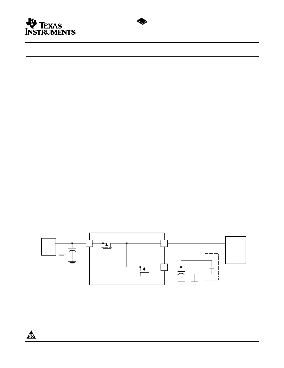
POWER FLOW DIAGRAM
(1)
IN
BAT
OUT
bq24070
PACK+
PACK!
System
VDC
GND
AC Adapter
+
Q1
Q2
UDG
-04082
40 m
(2)
bq24070
SLUS694A MARCH 2006 REVISED MARCH 2006
SINGLE-CHIP CHARGE AND SYSTEM POWER-PATH MANAGEMENT IC
·
Small 3,5 mm × 4,5 mm QFN Package
The bq24070 device is a highly integrated Li-ion
linear charger and system power-path management
·
Designed for Single-Cell Li-Ion- or
device
targeted
at
space-limited
portable
Li-Polymer-Based Portable Applications
applications. The bq24070 offers DC supply (AC
·
Integrated Dynamic Power-Path Management
adapter) power-path management with autonomous
(DPPM) Feature Allowing the AC Adapter to
power-source selection, power FETs and current
Simultaneously Power the System and
sensors,
high-accuracy
current
and
voltage
Charge the Battery
regulation, charge status, and charge termination, in
a single monolithic device.
·
Power Supplement Mode Allows Battery to
Supplement the AC Input Current
The bq24070 powers the system while independently
·
Autonomous Power Source Selection (AC
charging the battery. This feature reduces the charge
Adapter or BAT)
and discharge cycles on the battery, allows for
proper charge termination and allows the system to
·
Supports Up to 2-A Total Current
run with an absent or defective battery pack. This
·
Thermal Regulation for Charge Control
feature also allows for the system to instantaneously
·
Charge Status Outputs for LED or System
turn on from an external power source in the case of
a deeply discharged battery pack. The IC design is
Interface Indicates Charge and Fault
focused on supplying continuous power to the
Conditions
system when available from the AC adapter or
·
Reverse Current, Short-Circuit, and Thermal
battery sources.
Protection
·
Power Good Status Outputs
·
Smart Phones and PDA
·
MP3 Players
·
Digital Cameras and Handheld Devices
·
Internet Appliances
(1)
See Figure 2 and functional block diagram for more detailed feature information.
(2)
P-FET back gate body diodes are disconnected to prevent body diode conduction.
Please be aware that an important notice concerning availability, standard warranty, and use in critical applications of Texas
Instruments semiconductor products and disclaimers thereto appears at the end of this data sheet.
PRODUCTION DATA information is current as of publication date.
Copyright © 2006, Texas Instruments Incorporated
Products conform to specifications per the terms of the Texas
Instruments standard warranty. Production processing does not
necessarily include testing of all parameters.
www.ti.com
DESCRIPTION (CONTINUED)
bq24070
SLUS694A MARCH 2006 REVISED MARCH 2006
These devices have limited built-in ESD protection. The leads should be shorted together or the device placed in conductive foam
during storage or handling to prevent electrostatic damage to the MOSFET gates.
The MODE pin selects the priority of the input sources. If an input source is not available, then the battery is
selected as the source. With the MODE pin high, the bq24070 attempts to charge from the input at the charge
rate set by ISET1 pin. With the MODE pin low, the bq24070 defaults to USB charging at the charge rate. This
feature allows the use of a single connector (mini-USB cable), where the host programs the MODE pin
according to the source that is connected (AC adaptor or USB port).
Table 1
summarizes the MODE pin
function.
Table 1. Power Source Selection Function Summary
MODE STATE
AC
MAXIMUM
SYSTEM
USB BOOT-UP
ADAPTER
CHARGE RATE
(1)
POWER
FEATURE
SOURCE
Low
Present
ISET2
USB
Enabled
Absent
N/A
Battery
Disabled
High
Present
ISET1
AC
Disabled
Absent
N/A
Battery
Disabled
(1)
Battery charge rate is always set by ISET1, but may be reduced by a limited input source (ISET2 USB mode) and I
OUT
system load.
ORDERING INFORMATION
(1)
BATTERY
PART
PACKAGE
T
A
OUT PIN
STATUS
VOLTAGE (V)
NUMBER
(2) (3)
MARKING
4.2
Regulated to 4.4 V
(4)
bq24070RHLR
Production
BRQ
40°C to 125°C
4.2
Regulated to 4.4 V
(4)
bq24070RHLT
Production
BRQ
(1)
For the most current package and ordering information, see the Package Option Addendum at the end of this document, or see the TI
Web site at
www.ti.com.
(2)
The RHL package is available in the following options:
R - taped and reeled in quantities of 3,000 devices per reel.
T - taped and reeled in quantities of 250 devices per reel.
(3)
This product is RoHS compatible, including a lead concentration that does not exceed 0.1% of total product weight, and is suitable for
use in specified lead-free soldering processes. In addition, this product uses package materials that do not contain halogens, including
bromine (Br) or antimony (Sb) above 0.1% of total product weight.
(4)
If AC < V
O(OUT-REG)
, the AC is connected to the OUT pin by a P-FET, (Q1).
2
Submit Documentation Feedback
www.ti.com
ABSOLUTE MAXIMUM RATINGS
(1)
RECOMMENDED OPERATING CONDITIONS
DISSIPATION RATINGS
bq24070
SLUS694A MARCH 2006 REVISED MARCH 2006
over operating free-air temperature range (unless otherwise noted)
bq24070
Input voltage
IN (DC voltage wrt (with respect to) VSS)
0.3 V to 18 V
BAT, CE, DPPM, PG, Mode, OUT, ISET1, ISET2, STAT1,
0.3 V to 7 V
STAT2, TS, (all DC voltages wrt VSS)
Input voltage
V
REF
(DC voltage wrt VSS)
0.3 V to V
O(OUT)
+ 0.3 V
TMR
0.3 V to V
O
+ 0.3 V
Input current
3.5 A
OUT
4 A
Output current
BAT
(2)
4 A to 3.5 A
Output sink current
PG, STAT1, STAT2,
1.5 mA
Storage temperature range, T
stg
65°C to 150°C
Junction temperature range, T
J
40°C to 150°C
Lead temperature (soldering, 10 seconds)
300°C
(1)
Stresses beyond those listed under absolute maximum ratings may cause permanent damage to the device. These are stress ratings
only, and functional operation of the device at these or any other conditions beyond those indicated under recommended operating
conditions is not implied. Exposure to absolute-maximum-rated conditions for extended periods may affect device reliability. All voltage
values are with respect to the network ground terminal unless otherwise noted.
(2)
Negative current is defined as current flowing into the BAT pin.
MIN
MAX
UNIT
V
CC
Supply voltage (V
IN
)
(1)
4.35
16
V
I
AC
Input current
2
A
T
J
Operating junction temperature range
40
125
°C
(1)
Verify that power dissipation and junction temperatures are within limits at maximum V
CC
.
T
A
40°C
DERATING FACTOR
PACKAGE
JA
POWER RATING
T
A
> 40°C
20-pin RHL
(1)
1.81 W
21 mW/°C
46.87 °C/W
(1)
This data is based on using the JEDEC High-K board and the exposed die pad is connected to a Cu pad on the board. This is
connected to the ground plane by a 2×3 via matrix.
3
Submit Documentation Feedback
www.ti.com
ELECTRICAL CHARACTERISTICS
bq24070
SLUS694A MARCH 2006 REVISED MARCH 2006
over junction temperature range (0°C
T
J
125°C) and the recommended supply voltage range (unless otherwise noted)
PARAMETER
TEST CONDITIONS
MIN
TYP
MAX
UNIT
INPUT BIAS CURRENTS
I
CC(SPLY)
Active supply current, VCC
V
VCC
> V
VCC(min)
1
2
mA
V
IN
< V
(BAT)
Sleep current (current into BAT
I
CC(SLP)
2.6 V
V
I(BAT)
V
O(BAT-REG)
,
2
5
pin)
Excludes load on OUT pin
V
I(AC)
6V, Total current into IN pin with
I
CC(IN-STDBY)
Input standby current
chip disabled, Excludes all loads,
200
CE=LOW, after t
(CE-HOLDOFF)
delay
µA
Total current into BAT pin with input
present and chip disabled;
I
CC(BAT-STDBY)
BAT standby current
Excludes all loads, CE=LOW,
45
65
after t
(CE-HOLDOFF)
delay,
0°C
T
J
85°C
I
IB(BAT)
Charge done current, BAT
Charge DONE, input supplying the load
1
5
OUT PIN-VOLTAGE REGULATION
Output regulation
V
O(OUT-REG)
V
I(AC)
4.4 V+V
DO
4.4
4.5
V
voltage
OUT PIN DPPM REGULATION
V
(DPPM-SET)
DPPM set point
(1)
V
DPPM-SET
< V
OUT
2.6
3.8
V
I
(DPPM-SET)
DPPM current source
Input present
95
100
105
µA
SF
DPPM scale factor
V
(DPPM-REG)
= V
(DPPM-SET)
× SF
1.139
1.150
1.162
OUT PIN FET (Q1, Q2) DROP-OUT VOLTAGE ®
DS(on)
)
V
I(AC)
V
CC(min)
, Mode = High,
V
(ACDO)
AC to OUT dropout voltage
(2)
300
475
I
I(AC)
= 1 A, (I
O(OUT)
+ I
O(BAT)
), or no input
mV
BAT to OUT dropout voltage
V
(BATDO)
V
I (BAT)
3 V, I
i(BAT)
= 1.0 A, V
CC
< V
i(BAT)
40
100
(discharging)
OUT PIN - BATTERY SUPPLEMENT MODE
Enter battery supplement mode
V
I(OUT)
V
BSUP1
(battery supplements OUT current
V
I(BAT)
> 2 V
V
I(BAT)
in the presence of input source
60 mV
V
V
I(OUT)
V
BSUP2
Exit battery supplement mode
V
I(BAT)
> 2 V
V
I(BAT)
20 mV
OUT PIN - SHORT CIRCUIT
Current source between BAT to OUT for
I
OSH1
BAT to OUT short-circuit recovery
short-circuit recovery to
10
mA
V
I(OUT)
V
I(BAT)
200 mV
R
SHAC
AC to OUT short-circuit limit
V
I(OUT)
1 V
500
BAT PIN CHARGING PRECHARGE
Precharge to fast-charge transition
V
(LOWV)
Voltage on BAT
2.9
3
3.1
V
threshold
Deglitch time for fast-charge to
t
FALL
= 100 ns, 10 mV overdrive,
T
DGL(F)
22.5
ms
precharge transition
(3)
V
I(BAT)
decreasing below threshold
1 V < V
I(BAT)
< V
(LOWV)
, t < t
(PRECHG)
,
I
O(PRECHG)
Precharge range
10
150
mA
I
O(PRECHG)
= (K
(SET)
× V
(PRECHG)
)/ R
SET
V
(PRECHG)
Precharge set voltage
1 V < V
I(BAT)
< V
(LOWV)
, t < t
(PRECHG)
225
250
275
mV
BAT PIN CHARGING - CURRENT REGULATION
V
i (BAT)
> V
(LOWV)
, Mode = High
I
O(BAT)
Battery charge current range
(4)
I
OUT(BAT)
= (K
(SET)
× V
(SET)
/ R
SET
),
100
1000
1500
mA
V
I
(OUT) > V
O
(OUT-REG) + V
(DO-MAX)
R
PBAT
BAT to OUT pullup
V
i (BAT)
< 1 V
1000
(1)
V
(DPPM-SET)
is scaled up by the scale factor for controlling the output voltage V
(DPPM-REG)
.
(2)
V
DO(max)
, dropout voltage is a function of the FET, R
DS(on)
, and drain current. The dropout voltage increases proportionally to the
increase in current.
(3)
All deglitch periods are a function of the timer setting and is modified in DPPM or thermal regulation modes by the percentages that the
program current is reduced.
(4)
When input current remains below 2 A, the battery charging current may be raised until the thermal regulation limits the charge current.
4
Submit Documentation Feedback
www.ti.com
bq24070
SLUS694A MARCH 2006 REVISED MARCH 2006
ELECTRICAL CHARACTERISTICS (continued)
over junction temperature range (0°C
T
J
125°C) and the recommended supply voltage range (unless otherwise noted)
PARAMETER
TEST CONDITIONS
MIN
TYP
MAX
UNIT
Voltage on ISET1, V
VCC
4.35 V,
Battery charge current set
V
(SET)
V
I(OUT)
- V
I(BAT)
> V
(DO-MAX)
,
2.47
2.50
2.53
V
voltage
(5)
V
I(BAT)
> V
(LOWV)
100 mA
I
O(BAT)
1.5 A
375
425
450
K
(SET)
Charge current set factor, BAT
10 mA
I
O(BAT)
100 mA
(6)
300
450
600
USB MODE INPUT CURRENT LIMIT
ISET2 = Low
80
90
100
I
(USB)
USB input port current range
mA
ISET2 = High
400
500
BAT PIN CHARGING VOLTAGE REGULATION, V
O (BAT-REG)
+ V
(DO-MAX)
< V
CC
, I
TERM
< I
BAT(OUT)
1 A
Battery charge voltage
4.2
V
V
O(BAT-REG)
T
A
= 25°C
0.5%
0.5%
Battery charge voltage regulation
accuracy
1%
1%
CHARGE TERMINATION DETECTION
Charge termination detection
V
I(BAT)
> V
(RCH)
,
I
(TERM)
10
150
mA
range
I
(TERM)
= (K
(SET)
× V
(TERM)
)/ R
SET
V
I(BAT)
> V
(RCH)
, Mode = High
230
250
270
Charge termination set voltage,
V
(TERM)
mV
measured on ISET1
V
I(BAT)
> V
(RCH)
, Mode = Low
95
100
130
t
FALL
= 100 ns, 10 mV overdrive,
Deglitch time for termination
T
DGL(TERM)
I
CHG
increasing above or decreasing
22.5
ms
detection
below threshold
TEMPERATURE SENSE COMPARATORS
V
LTF
High voltage threshold
Temp fault at V(TS) > V
LTF
2.465
2.500
2.535
V
V
HTF
Low voltage threshold
Temp fault at V(TS) < V
HTF
0.485
0.500
0.515
V
I
TS
Temperature sense current source
94
100
106
µA
R
(TMR)
= 50 k
, V
I(BAT)
increasing or
Deglitch time for temperature fault
T
DGL(TF)
decreasing above and below;
22.5
ms
detection
(7)
100-ns fall time, 10-mv overdrive
BATTERY RECHARGE THRESHOLD
V
O(BAT-REG)
V
O(BAT-REG)
V
O(BAT-REG)
V
RCH
Recharge threshold voltage
V
0.075
0.100
0.125
R
(TMR)
= 50 k
, V
I(BAT)
increasing
Deglitch time for recharge
T
DGL(RCH)
or decreasing below threshold,
22.5
ms
detection
(7)
100-ns fall time, 10-mv overdrive
STAT1, STAT2, AND PG, OPEN DRAIN (OD) OUTPUTS
(8)
I
OL
= 5 mA, An external pullup
V
OL
Low-level output saturation voltage
0.25
V
resistor
1 K required.
I
LKG
Input leakage current
1
5
µA
ISET2, CE INPUTS
V
IL
Low-level input voltage
0
0.4
V
V
IH
High-level input voltage
1.4
I
IL
Low-level input current, CE
1
I
IH
High-level input current, CE
1
µA
I
IL
Low-level input current, ISET2
V
ISET2
= 0.4 V
20
I
IH
High-level input current, ISET2
V
ISET2
= V
CC
40
t
(CE-HLDOFF)
Holdoff time, CE
CE going low only
4
6
ms
MODE INPUT
Falling Hi
Low; 280 K ± 10% applied
V
IL
Low-level input voltage
0.975
1
1.025
V
when low.
V
IH
High-level input voltage
Input R
Mode
sets external hysteresis
V
IL
+ .01
V
IL
+ .024
V
I
IL
Low-level input current, Mode
1
µA
(5)
For half-charge rate, V
(SET)
is 1.25 V ± 25 mV.
(6)
Specification is for monitoring charge current via the ISET1 pin during voltage regulation mode, not for a reduced fast-charge level.
(7)
All deglitch periods are a function of the timer setting and is modified in DPPM or thermal regulation modes by the percentages that the
program current is reduced.
(8)
See Charger Sleep mode for PG (V
CC
= V
IN
) specifications.
5
Submit Documentation Feedback
Document Outline