 | ÐлекÑÑоннÑй компоненÑ: CDC208 | СкаÑаÑÑ:  PDF PDF  ZIP ZIP |
Äîêóìåíòàöèÿ è îïèñàíèÿ www.docs.chipfind.ru
CDC208
DUAL 1-LINE TO 4-LINE CLOCK DRIVER
WITH 3-STATE OUTPUTS
SCAS109F APRIL 1990 REVISED OCTOBER 1998
1
POST OFFICE BOX 655303
·
DALLAS, TEXAS 75265
D
Low-Skew Propagation Delay
Specifications for Clock-Driver
Applications
D
TTL-Compatible Inputs and
CMOS-Compatible Outputs
D
Flow-Through Architecture Optimizes
PCB Layout
D
Center-Pin V
CC
and GND Pin
Configurations Minimize High-Speed
Switching Noise
D
EPIC
TM
(Enhanced-Performance Implanted
CMOS) 1-
µ
m Process
D
500-mA Typical Latch-Up Immunity at
125
°
C
D
Package Options Include Plastic
Small-Outline (DW)
description
The CDC208 contains dual clock-driver circuits that fanout one input signal to four outputs with minimum skew
for clock distribution (see Figure 2). The device also offers two output-enable (OE1 and OE2) inputs for each
circuit that can force the outputs to be disabled to a high-impedance state or to a high- or low-logic level
independent of the signal on the respective A input.
Skew parameters are specified for a reduced temperature and voltage range common to many applications.
The CDC208 is characterized for operation from 40
°
C to 85
°
C.
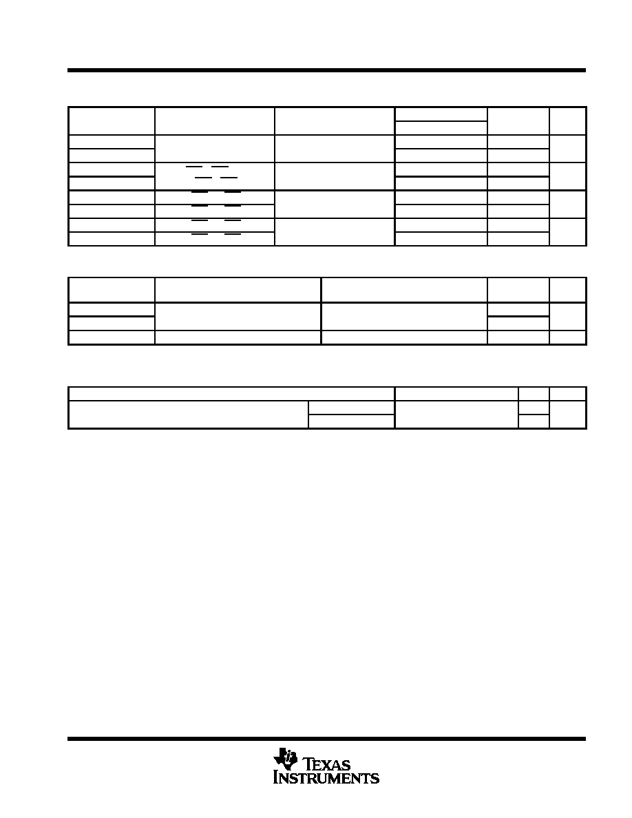
FUNCTION TABLES
INPUTS
OUTPUTS
1OE1
1OE2
1A
1Y1
1Y2
1Y3
1Y4
L
L
L
L
L
L
L
L
L
H
H
H
H
H
L
H
X
L
L
L
L
H
L
X
H
H
H
H
H
H
X
Z
Z
Z
Z
INPUTS
OUTPUTS
2OE1
2OE2
2A
2Y1
2Y2
2Y3
2Y4
L
L
L
L
L
L
L
L
L
H
H
H
H
H
L
H
X
L
L
L
L
H
L
X
H
H
H
H
H
H
X
Z
Z
Z
Z
Copyright
©
1998, Texas Instruments Incorporated
PRODUCTION DATA information is current as of publication date.
Products conform to specifications per the terms of Texas Instruments
standard warranty. Production processing does not necessarily include
testing of all parameters.
Please be aware that an important notice concerning availability, standard warranty, and use in critical applications of
Texas Instruments semiconductor products and disclaimers thereto appears at the end of this data sheet.
EPIC is a trademark of Texas Instruments Incorporated.
1
2
3
4
5
6
7
8
9
10
20
19
18
17
16
15
14
13
12
11
1Y2
1Y3
1Y4
GND
GND
GND
GND
2Y1
2Y2
2Y3
1Y1
1A
1OE1
1OE2
V
CC
V
CC
2A
2OE1
2OE2
2Y4
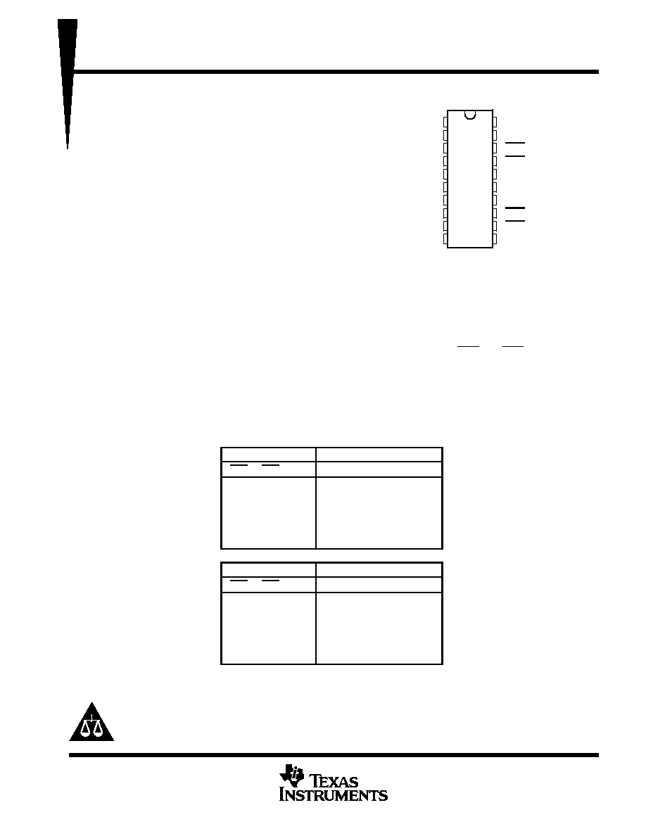
DW PACKAGE
(TOP VIEW)
CDC208
DUAL 1-LINE TO 4-LINE CLOCK DRIVER
WITH 3-STATE OUTPUTS
SCAS109F APRIL 1990 REVISED OCTOBER 1998
2
POST OFFICE BOX 655303
·
DALLAS, TEXAS 75265
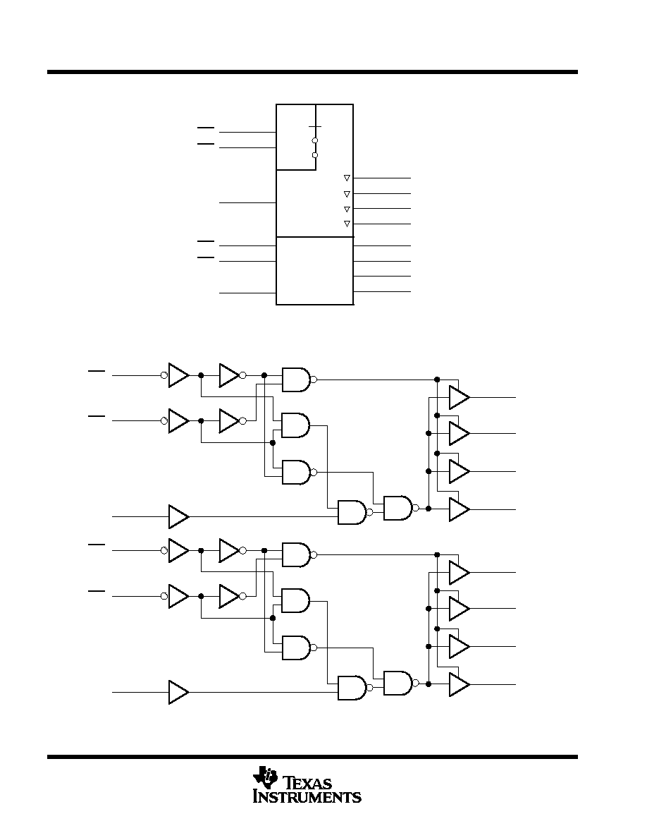
logic symbol
X/Y
19
1A
1
18
2
17
1Y1
20
1Y2
1
1Y3
2
1Y4
3
1
1
2
3
G5
EN
2Y1
8
2Y2
9
2Y3
10
2Y4
11
13
12
14
2A
4, 5
1OE1
1OE2
2OE1
2OE2
4, 5
4, 5
4, 5
V4
This symbol is in accordance with ANSI/IEEE Std 91-1984 and IEC Publication 617-12.
logic diagram (positive logic)
1Y1
20
1OE1
18
1OE2
17
1A
19
1Y2
1
1Y3
2
1Y4
3
2Y1
8
2OE1
13
2OE2
12
2A
14
2Y2
9
2Y3
10
2Y4
11
CDC208
DUAL 1-LINE TO 4-LINE CLOCK DRIVER
WITH 3-STATE OUTPUTS
SCAS109F APRIL 1990 REVISED OCTOBER 1998
3
POST OFFICE BOX 655303
·
DALLAS, TEXAS 75265
absolute maximum ratings over operating free-air temperature range (unless otherwise noted)
Supply voltage range, V
CC
0.5 V to 7 V
. . . . . . . . . . . . . . . . . . . . . . . . . . . . . . . . . . . . . . . . . . . . . . . . . . . . . . . . . .
Input voltage range, V
I
(see Note 1)
0.5 V to V
CC
+ 0.5 V
. . . . . . . . . . . . . . . . . . . . . . . . . . . . . . . . . . . . . . . . . .
Output voltage range, V
O
(see Note 1)
0.5 V to V
CC
+ 0.5 V
. . . . . . . . . . . . . . . . . . . . . . . . . . . . . . . . . . . . . . .
Input clamp current, I
IK
(V
I
< 0 or V
I
> V
CC
)
±
20 mA
. . . . . . . . . . . . . . . . . . . . . . . . . . . . . . . . . . . . . . . . . . . . . . . .
Output clamp current, I
OK
(V
O
< 0 or V
O
> V
CC
)
±
50 mA
. . . . . . . . . . . . . . . . . . . . . . . . . . . . . . . . . . . . . . . . . . . .
Continuous output current, I
O
(V
O
= 0 to V
CC
)
±
50 mA
. . . . . . . . . . . . . . . . . . . . . . . . . . . . . . . . . . . . . . . . . . . . . .
Continuous current through V
CC
or GND
±
200 mA
. . . . . . . . . . . . . . . . . . . . . . . . . . . . . . . . . . . . . . . . . . . . . . . . . .
Maximum power dissipation at T
A
= 55
°
C (in still air) (see Note 2)
1.6 W
. . . . . . . . . . . . . . . . . . . . . . . . . . . . . . .
Storage temperature range
65
°
C to 150
°
C
. . . . . . . . . . . . . . . . . . . . . . . . . . . . . . . . . . . . . . . . . . . . . . . . . . . . . . . .
Stresses beyond those listed under "absolute maximum ratings" may cause permanent damage to the device. These are stress ratings only, and
functional operation of the device at these or any other conditions beyond those indicated under "recommended operating conditions" is not
implied. Exposure to absolute-maximum-rated conditions for extended periods may affect device reliability.
NOTES:
1. The input and output negative-voltage ratings may be exceeded if the input and output clamp-current ratings are observed.
2. The maximum package power dissipation is calculated using a junction temperature of 150
°
C and a board trace length of 750 mils.
For more information, refer to the
Package Thermal Considerations application note in the 1994 ABT Advanced BiCMOS Technology
Data Book, literature number SCBD002B.
recommended operating conditions
MIN
NOM
MAX
UNIT
VCC
Supply voltage
4.5
5
5.5
V
VIH
High-level input voltage
2
V
VIL
Low-level input voltage
0.8
V
VI
Input voltage
0
VCC
V
IOH
High-level output current
24
mA
IOL
Low-level output current
24
mA
t /
v
Input transition rise or fall rate
0
10
ns / V
fclock
Input clock frequency
60
MHz
TA
Operating free-air temperature
40
85
°
C
CDC208
DUAL 1-LINE TO 4-LINE CLOCK DRIVER
WITH 3-STATE OUTPUTS
SCAS109F APRIL 1990 REVISED OCTOBER 1998
4
POST OFFICE BOX 655303
·
DALLAS, TEXAS 75265
electrical characteristics over recommended operating free-air temperature range (unless
otherwise noted)
PARAMETER
TEST CONDITIONS
VCC
TA = 25
°
C
MIN
MAX
UNIT
PARAMETER
TEST CONDITIONS
VCC
MIN
TYP
MAX
MIN
MAX
UNIT
IOH = 50
µ
A
4.5 V
4.4
4.4
IOH = 50
µ
A
5.5 V
5.4
5.4
VOH
IOH = 24 mA
4.5 V
3.94
3.8
V
IOH = 24 mA
5.5 V
4.94
4.8
IOH = 75 mA
5.5 V
3.85
IOL = 50
µ
A
4.5 V
0.1
0.1
IOL = 50
µ
A
5.5 V
0.1
0.1
VOL
IOL = 24 mA
4.5 V
0.36
0.44
V
IOL = 24 mA
5.5 V
0.36
0.44
IOL = 75 mA
5.5 V
1.65
II
VI = VCC or GND
5.5 V
±
0.1
±
1
µ
A
IOZ
VO = VCC or GND
5.5 V
±
0.5
±
5
µ
A
ICC
VI = VCC or GND,
IO = 0
5.5 V
8
80
µ
A
ICC
One input at 3.4 V,
Other inputs at VCC or GND
5.5 V
0.9
1
mA
Ci
VI = VCC or GND
5 V
4
pF
Co
VO = VCC or GND
5 V
10
pF
Not more than one output should be tested at a time, and the duration of the test should not exceed 10 ms.
This is the increase in supply current for each input that is at one of the specified TTL voltage levels rather than 0 V or VCC.
CDC208
DUAL 1-LINE TO 4-LINE CLOCK DRIVER
WITH 3-STATE OUTPUTS
SCAS109F APRIL 1990 REVISED OCTOBER 1998
5
POST OFFICE BOX 655303
·
DALLAS, TEXAS 75265
switching characteristics over recommended operating free-air temperature range,
V
CC
= 5 V
±
0.5 V (unless otherwise noted) (see Figure 1)
PARAMETER
FROM
TO
TA = 25
°
C
MIN
MAX
UNIT
PARAMETER
(INPUT)
(OUTPUT)
MIN
TYP
MAX
MIN
MAX
UNIT
tPLH
1A and 2A
Any Y
5.3
8.5
10.9
5.3
11.7
ns
tPHL
1A and 2A
Any Y
3.6
7.7
11
3.6
11.5
ns
tPLH
1OE1, 1OE2, and
Any Y
4.7
8.5
11.7
4.7
12.8
ns
tPHL
,
,
2OE1, 2OE2
Any Y
4.4
8.4
11.3
4.4
12.4
ns
tPZH
1OE2 or 2OE2
Any Y
4.4
8.1
11.3
4.4
12.4
ns
tPZL
1OE1 or 2OE1
Any Y
5
9.6
13.3
5
14.9
ns
tPHZ
1OE2 or 2OE2
Any Y
4.2
7.4
9.3
4.2
10.2
ns
tPLZ
1OE1 or 2OE1
Any Y
5.4
7.5
9.2
5.4
9.9
ns
switching characteristics, V
CC
= 5 V
±
0.25 V, T
A
= 25
°
C to 70
°
C (see Note 3 and Figures 1 and 2)
PARAMETER
FROM
(INPUT)
TO
(OUTPUT)
MIN
MAX
UNIT
tPLH
1A and 2A
Any Y
6.6
10.2
ns
tPHL
1A and 2A
Any Y
6.6
9.8
ns
tsk(o)
1A and 2A
Any Y
1
ns
NOTE 3: All specifications are valid only for all outputs switching simultaneously and in phase.
operating characteristics, V
CC
= 5 V, T
A
= 25
°
C
PARAMETER
TEST CONDITIONS
TYP
UNIT
C d
Power dissipation capacitance per bank
Outputs enabled
CL = 50 pF
f = 1 MHz
96
pF
Cpd
Power dissipation capacitance per bank
Outputs disabled
CL = 50 pF, f = 1 MHz
12
pF
CDC208
DUAL 1-LINE TO 4-LINE CLOCK DRIVER
WITH 3-STATE OUTPUTS
SCAS109F APRIL 1990 REVISED OCTOBER 1998
6
POST OFFICE BOX 655303
·
DALLAS, TEXAS 75265
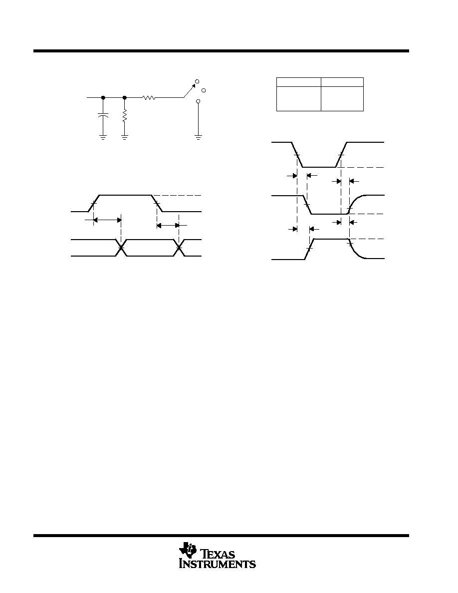
PARAMETER MEASUREMENT INFORMATION
From Output
Under Test
CL = 50 pF
(see Note A)
LOAD CIRCUIT FOR OUTPUTS
S1
2
×
VCC
Open
GND
500
500
TEST
tPLH/tPHL
tPLZ/tPZL
tPHZ/tPZH
S1
Open
2
×
VCC
GND
Output
Control
(low-level
enabling)
Output
Waveform 1
S1 at 2
×
VCC
(see Note C)
Output
Waveform 2
S1 at 2
×
VCC
(see Note C)
VOL
VOH
tPZL
tPZH
tPLZ
tPHZ
1.5 V
1.5 V
VCC
0 V
50% VCC
0 V
3 V
(see Note A)
50% VCC
20% VCC
80% VCC
tPLH
tPHL
1.5 V
1.5 V
3 V
0 V
50% VCC
50% VCC
VOH
VOL
Input
(see Note B)
Output
VOLTAGE WAVEFORMS
PROPAGATION DELAY TIMES
VOLTAGE WAVEFORMS
ENABLE AND DISABLE TIMES
NOTES: A. CL includes probe and jig capacitance.
B. All input pulses are supplied by generators having the following characteristics: PRR
10 MHz, ZO = 50
, tr
3 ns, tf
3 ns.
For testing pulse duration: tr = tf = 1 to 3 ns. Pulse polarity can be either high-to-low-to-high or low-to-high-to-low.
C. Waveform 1 is for an output with internal conditions such that the output is low except when disabled by the output control.
Waveform 2 is for an output with internal conditions such that the output is high except when disabled by the output control.
Figure 1. Load Circuit and Voltage Waveforms
CDC208
DUAL 1-LINE TO 4-LINE CLOCK DRIVER
WITH 3-STATE OUTPUTS
SCAS109F APRIL 1990 REVISED OCTOBER 1998
7
POST OFFICE BOX 655303
·
DALLAS, TEXAS 75265
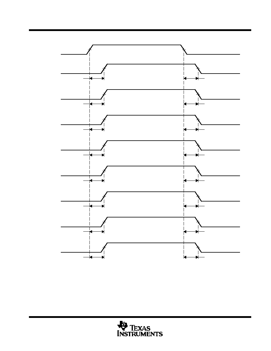
PARAMETER MEASUREMENT INFORMATION
1A, 2A
1Y1
1Y2
1Y3
1Y4
2Y1
2Y2
2Y3
2Y4
tPLH1
tPLH2
tPLH3
tPLH4
tPLH5
tPLH6
tPLH7
tPLH8
tPHL1
tPHL2
tPHL3
tPHL4
tPHL5
tPHL6
tPHL7
tPHL8
NOTE A: Output skew, tsk(o), is calculated as the greater of:
The difference between the fastest and slowest of tPLHn (n = 1, 2, . . . , 8)
The difference between the fastest and slowest of tPHLn (n = 1, 2, . . . , 8)
Figure 2. Waveforms for Calculation of t
sk(o)
CDC208
DUAL 1-LINE TO 4-LINE CLOCK DRIVER
WITH 3-STATE OUTPUTS
SCAS109F APRIL 1990 REVISED OCTOBER 1998
8
POST OFFICE BOX 655303
·
DALLAS, TEXAS 75265
MECHANICAL INFORMATION
DW (R-PDSO-G**)
PLASTIC SMALL-OUTLINE PACKAGE
16 PIN SHOWN
4040000 / D 02/98
Seating Plane
0.400 (10,15)
0.419 (10,65)
0.104 (2,65) MAX
1
0.012 (0,30)
0.004 (0,10)
A
8
16
0.020 (0,51)
0.014 (0,35)
0.293 (7,45)
0.299 (7,59)
9
0.010 (0,25)
0.050 (1,27)
0.016 (0,40)
(15,24)
(15,49)
PINS **
0.010 (0,25) NOM
A MAX
DIM
A MIN
Gage Plane
20
0.500
(12,70)
(12,95)
0.510
(10,16)
(10,41)
0.400
0.410
16
0.600
24
0.610
0.004 (0,10)
M
0.010 (0,25)
0.050 (1,27)
0
°
8
°
NOTES: A. All linear dimensions are in inches (millimeters).
B. This drawing is subject to change without notice.
C. Body dimensions do not include mold flash or protrusion not to exceed 0.006 (0,15).
D. Falls within JEDEC MS-013
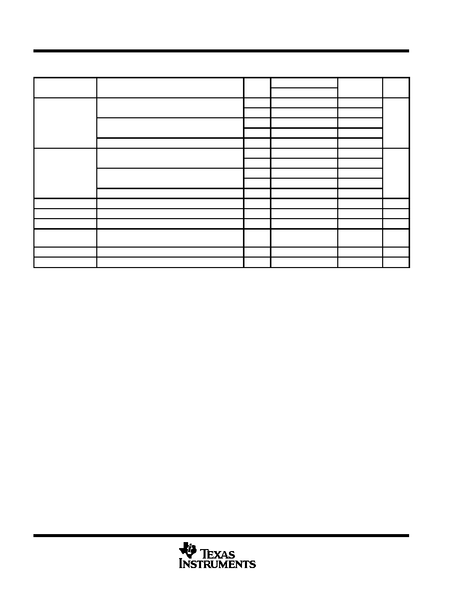
PACKAGING INFORMATION
Orderable Device
Status
(1)
Package
Type
Package
Drawing
Pins Package
Qty
Eco Plan
(2)
Lead/Ball Finish
MSL Peak Temp
(3)
CDC208DBLE
OBSOLETE
SSOP
DB
20
TBD
Call TI
Call TI
CDC208DW
ACTIVE
SOIC
DW
20
25
Green (RoHS &
no Sb/Br)
CU NIPDAU
Level-1-260C-UNLIM
CDC208DWG4
ACTIVE
SOIC
DW
20
25
Green (RoHS &
no Sb/Br)
CU NIPDAU
Level-1-260C-UNLIM
CDC208DWR
ACTIVE
SOIC
DW
20
2000 Green (RoHS &
no Sb/Br)
CU NIPDAU
Level-1-260C-UNLIM
CDC208DWRG4
ACTIVE
SOIC
DW
20
2000 Green (RoHS &
no Sb/Br)
CU NIPDAU
Level-1-260C-UNLIM
CDC208N
OBSOLETE
PDIP
N
20
TBD
Call TI
Call TI
(1)
The marketing status values are defined as follows:
ACTIVE: Product device recommended for new designs.
LIFEBUY: TI has announced that the device will be discontinued, and a lifetime-buy period is in effect.
NRND: Not recommended for new designs. Device is in production to support existing customers, but TI does not recommend using this part in
a new design.
PREVIEW: Device has been announced but is not in production. Samples may or may not be available.
OBSOLETE: TI has discontinued the production of the device.
(2)
Eco
Plan
-
The
planned
eco-friendly
classification:
Pb-Free
(RoHS)
or
Green
(RoHS
&
no
Sb/Br)
-
please
check
http://www.ti.com/productcontent
for the latest availability information and additional product content details.
TBD: The Pb-Free/Green conversion plan has not been defined.
Pb-Free (RoHS): TI's terms "Lead-Free" or "Pb-Free" mean semiconductor products that are compatible with the current RoHS requirements
for all 6 substances, including the requirement that lead not exceed 0.1% by weight in homogeneous materials. Where designed to be soldered
at high temperatures, TI Pb-Free products are suitable for use in specified lead-free processes.
Green (RoHS & no Sb/Br): TI defines "Green" to mean Pb-Free (RoHS compatible), and free of Bromine (Br) and Antimony (Sb) based flame
retardants (Br or Sb do not exceed 0.1% by weight in homogeneous material)
(3)
MSL, Peak Temp. -- The Moisture Sensitivity Level rating according to the JEDEC industry standard classifications, and peak solder
temperature.
Important Information and Disclaimer:The information provided on this page represents TI's knowledge and belief as of the date that it is
provided. TI bases its knowledge and belief on information provided by third parties, and makes no representation or warranty as to the
accuracy of such information. Efforts are underway to better integrate information from third parties. TI has taken and continues to take
reasonable steps to provide representative and accurate information but may not have conducted destructive testing or chemical analysis on
incoming materials and chemicals. TI and TI suppliers consider certain information to be proprietary, and thus CAS numbers and other limited
information may not be available for release.
In no event shall TI's liability arising out of such information exceed the total purchase price of the TI part(s) at issue in this document sold by TI
to Customer on an annual basis.
PACKAGE OPTION ADDENDUM
www.ti.com
17-Nov-2005
Addendum-Page 1

IMPORTANT NOTICE
Texas Instruments Incorporated and its subsidiaries (TI) reserve the right to make corrections, modifications,
enhancements, improvements, and other changes to its products and services at any time and to discontinue
any product or service without notice. Customers should obtain the latest relevant information before placing
orders and should verify that such information is current and complete. All products are sold subject to TI's terms
and conditions of sale supplied at the time of order acknowledgment.
TI warrants performance of its hardware products to the specifications applicable at the time of sale in
accordance with TI's standard warranty. Testing and other quality control techniques are used to the extent TI
deems necessary to support this warranty. Except where mandated by government requirements, testing of all
parameters of each product is not necessarily performed.
TI assumes no liability for applications assistance or customer product design. Customers are responsible for
their products and applications using TI components. To minimize the risks associated with customer products
and applications, customers should provide adequate design and operating safeguards.
TI does not warrant or represent that any license, either express or implied, is granted under any TI patent right,
copyright, mask work right, or other TI intellectual property right relating to any combination, machine, or process
in which TI products or services are used. Information published by TI regarding third-party products or services
does not constitute a license from TI to use such products or services or a warranty or endorsement thereof.
Use of such information may require a license from a third party under the patents or other intellectual property
of the third party, or a license from TI under the patents or other intellectual property of TI.
Reproduction of information in TI data books or data sheets is permissible only if reproduction is without
alteration and is accompanied by all associated warranties, conditions, limitations, and notices. Reproduction
of this information with alteration is an unfair and deceptive business practice. TI is not responsible or liable for
such altered documentation.
Resale of TI products or services with statements different from or beyond the parameters stated by TI for that
product or service voids all express and any implied warranties for the associated TI product or service and
is an unfair and deceptive business practice. TI is not responsible or liable for any such statements.
Following are URLs where you can obtain information on other Texas Instruments products and application
solutions:
Products
Applications
Amplifiers
amplifier.ti.com
Audio
www.ti.com/audio
Data Converters
dataconverter.ti.com
Automotive
www.ti.com/automotive
DSP
dsp.ti.com
Broadband
www.ti.com/broadband
Interface
interface.ti.com
Digital Control
www.ti.com/digitalcontrol
Logic
logic.ti.com
Military
www.ti.com/military
Power Mgmt
power.ti.com
Optical Networking
www.ti.com/opticalnetwork
Microcontrollers
microcontroller.ti.com
Security
www.ti.com/security
Telephony
www.ti.com/telephony
Video & Imaging
www.ti.com/video
Wireless
www.ti.com/wireless
Mailing Address:
Texas Instruments
Post Office Box 655303 Dallas, Texas 75265
Copyright
2005, Texas Instruments Incorporated