 | –≠–ª–µ–∫—Ç—Ä–æ–Ω–Ω—ã–π –∫–æ–º–ø–æ–Ω–µ–Ω—Ç: CDC930 | –°–∫–∞—á–∞—Ç—å:  PDF PDF  ZIP ZIP |
SCAS641
≠
JULY 2000
1
POST OFFICE BOX 655303 DALLAS, TEXAS 75265
Generates Clocks for Pentium 4
Microprocessors
Uses a 14.318 MHz Crystal Input to
Generate Multiple Output Frequencies
Includes Spread Spectrum Clocking (SSC),
0.6% Downspread for Reduced EMI With
Theoretical EMI Damping of 7 dB
Power Management Control Terminals
Low Output Skew and Jitter for Clock
Distribution
Operates From Single 3.3-V Supply
Consumes Less Than 30-mA Power-Down
Current
Generates the Following Clocks:
≠
4 HCLK (Host) (Different Pairs
≠
100/133 MHz)
≠
1 3VMREF Pair (3.3 V, 180 Shifted
50/66 MHz)
≠
10 PCI (3.3 V, 33.3 MHz)
≠
2 REF (3.3 V, 14.318 MHz)
≠
4 3V66 MHz (3.3 V, 66 MHz)
≠
2 3V48 MHz (3.3 V, 48 MHz)
Packaged in 56-Pin SSOP Package
description
The CDC930 is a differential clock synthesizer/
driver that generates HCLK/HCLK, 3VMREF/
3VMREF, PCI, 3V66, 3V48, REF system clock
signals to support a computer system with a
Pentium 4 microprocessor and a Direct
Rambus memory subsystem.
All output frequencies are generated from a 14.318-MHz crystal input. A reference clock input can be provided
at the XIN input instead of a crystal. Two phase-locked loops (PLLs) are used to generate the host frequencies
and the 48-MHz clock frequencies. On-chip loop filters and internal feedback eliminate the need for external
components. The host, PCI clock and 48-MHz clock outputs provide low-skew/low-jitter clock signals for reliable
clock operation. All outputs have 3-state capability, which can be selected using control inputs SEL133, SelA
and SelB.
The outputs are either differential host clock or 3.3-V single-ended CMOS buffers. When PWRDWN is set to
high, the device operates in normal mode. When PWRDWN is set low, the device transitions to a power-down
mode in which HCLK is driven at 2 I
REF
, HCLK is not driven, and all others are set low.
Copyright 2000, Texas Instruments Incorporated
Please be aware that an important notice concerning availability, standard warranty, and use in critical applications of
Texas Instruments semiconductor products and disclaimers thereto appears at the end of this data sheet.
This is system design dependant.
Intel and Pentium 4 are trademarks of Intel Corporation.
Rambus is a trademark of Rambus Corporation.
1
2
3
4
5
6
7
8
9
10
11
12
13
14
15
16
17
18
19
20
21
22
23
24
25
26
27
28
56
55
54
53
52
51
50
49
48
47
46
45
44
43
42
41
40
39
38
37
36
35
34
33
32
31
30
29
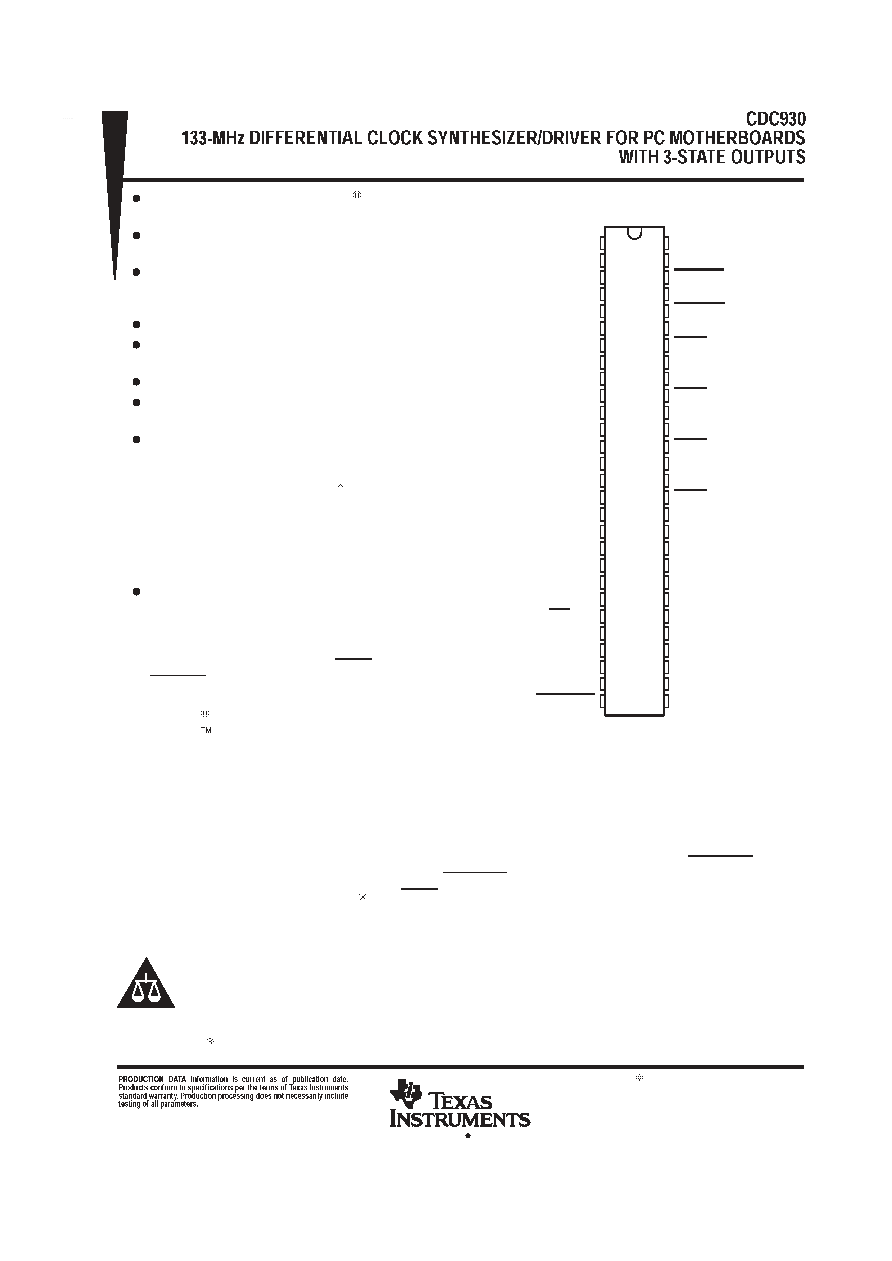
GND
REF0/MultSel0
REF1/MultSel1
V
DD
3.3V
XIN
XOUT
GND
PCI0
PCI1
V
DD
3.3V
PCI2
PCI3
GND
PCI4
PCI5
V
DD
3.3V
PCI6
PCI7
GND
PCI8
PCI9
V
DD
3.3V
SEL100/133
GND
3V48(0)/SelA
3V48(1)/SelB
V
DD
3.3V
PWRDWN
V
DD
3.3V
3VMREF
3VMREF
GND
SPREAD
HCLK(1)
HCLK(1)
V
DD
3.3V
HCLK(2)
HCLK(2)
GND
HCLK(3)
HCLK(3)
V
DD
3.3V
HCLK(4)
HCLK(4)
GND
I_REF
V
DD
3.3V
GND
V
DD
3.3V
3V66(0)
3V66(1)
GND
GND
3V66(2)
3V66(3)
V
DD
3.3V
DL PACKAGE
(TOP VIEW)

SCAS641
≠
JULY 2000
2
POST OFFICE BOX 655303 DALLAS, TEXAS 75265
description (continued)
The HOST bus operates at 100 MHz or 133 MHz. The MREF bus operates at 50 MHz or 66 MHz. Output
frequency selection is accomplished with corresponding setting for SEL100/133 control input. The PCI bus
frequency is fixed to 33 MHz.
Since the CDC930 is based on PLL circuitry, it requires a stabilization time to achieve phase-lock of the PLL.
This stabilization time is required following power up as well as changes to SEL inputs. With use of external
reference clock, this signal must be fixed-frequency and fixed-phase prior stabilization time starts.
functional block diagram
Control
Logic
3-State/Low
Test
SEL 100/133
Latched
2
Xtal
Oscillator
/3
/2
CPU
PLL
Spread
Logic
/2
48 MHz
PLL
/2
S
y
n
c
L
o
g
i
c
a
n
d
P
o
w
e
r
D
o
w
n
L
o
g
i
c
180
Phase
Shift
Latched
2
2*REF
14.318 MHz
(2,3)
2*3V48
48 MHz
(25,26)
10*PCI
33 MHz
(8,9,11,12,14,
15,17,18,20,21)
4*3V66
66 MHz
(30,31,34,35)
1*3VMREF
50/66 MHz
(55)
1*3VMREF
50/66 MHz
(54)
4*HCLK
100/133 MHz
(42,45,48,51)
4*HCLK
100/133 MHz
(41,44,47,50)
23
SEL100/133
25
SELA
26
SELB
5
XIN
6
XOUT
52
SPREAD
28
PWRDWN
2
MultSel0
3
MultSel1
39
I_REF
SCAS641
≠
JULY 2000
3
POST OFFICE BOX 655303 DALLAS, TEXAS 75265
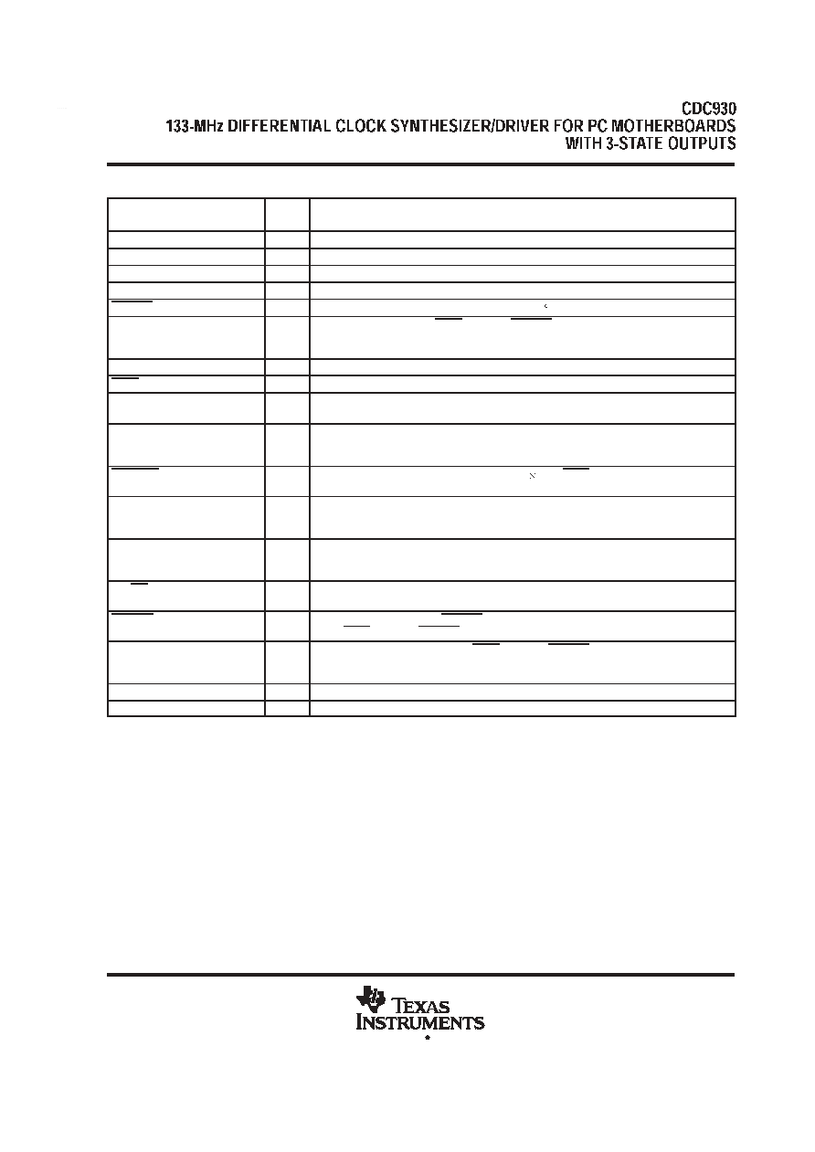
Terminal Functions
TERMINAL
I/O
DESCRIPTION
NAME
NO.
I/O
DESCRIPTION
3V48(0)/SelA
25
I/O
Dual function 3.3 V, Type 3, 48-MHz clock output that latches the state of SelA during power up
3V48(1)/SelB
26
I/O
Dual function 3.3 V, Type 3, 48-MHz clock output that latches the state of SelB during power up
3V66[0
≠
3]
30, 31, 34, 35
O
3.3 V, Type 5, 66-MHz clock outputs
3VMREF
55
O
3.3 V, Type 5, 50/66-MHz memory clock output
3VMREF
54
O
3.3 V, Type 5, 50/66-MHz memory clock output (180 out of phase with 3VMREF)
GND
1, 7, 13, 19,
24, 32, 33, 37,
40, 46, 53
Ground for core and HCLK/HCLK, 3VMREF/3VMREF, 3V48, 3V66 and PCI outputs
HCLK[1
≠
4]
42, 45, 48, 51
O
Type X1, host clock outputs
HCLK[1
≠
4]
41, 44, 47, 50
O
Type X1, host complementary clock outputs
I_REF
39
Special
Current reference pin for the host clock pairs. I_REF uses a fixed precision resistor tied to ground
to establish the appropriate current.
PCI[0
≠
9]
8, 9, 11, 12,
14, 15, 17, 18,
20, 21
O
3.3 V, Type 5, 33-MHz PCI clock outputs
PWRDWN
28
I
Power down for complete device with HOST at 2 IREF, HCLK not driven and all other outputs
forced low.
REF0/MultSel0
2
I/O
Dual function 3.3 V, Type 3, 14.318-MHz reference clock output. The state of MultSel0 is latched
during power up. MultSel0 configures the IOH amplitude (and thus the VOH swing amplitude) of
the HCLK pair outputs.
REF1/MultSel1
3
I/O
Dual function 3.3 V, Type 3, 14.318-MHz reference clock output. The state of MultSel1 is latched
during power up. MultSel1 configures the IOH amplitude (and thus the VOH swing amplitude) of
the HCLK pair outputs.
SEL100/133
23
I
Active low LVTTL level logic select. SEL100/133 is used for enabling 100/133 MHz. Low=100
MHz, high=133 MHz
SPREAD
52
I
LVTTL level logic select. SPREAD pin enables/disables the spread spectrum for the
HCLK/HCLK, 3VMREF/3VMREF, 3V66 and PCI outputs.
VDD3.3V
4, 10, 16, 22,
27, 29, 36, 38,
43, 49, 56
I
3.3-V power for core and the HCLK/HCLK, 3VMREF/3VMREF, 3V48, 3V66, and PCI outputs.
XIN
5
I
Crystal input
≠
14.318 MHz
XOUT
6
O
Crystal output
≠
14.318 MHz

SCAS641
≠
JULY 2000
4
POST OFFICE BOX 655303 DALLAS, TEXAS 75265
Function Tables
SELECT FUNCTIONS
INPUTS
OUTPUTS
FUNCTION
SEL100/133
SelA
SelB
HOST, HCLK
3VMREF, 3VMREF
PCI
3V66
3V48
REF
FUNCTION
0
0
0
100 MHz
50 MHz
33 MHz
66 MHz 48 MHz
14.318 MHz
Active 100 MHz
0
1
1
Hi-Z
Hi-Z
Hi-Z
Hi-Z
Hi-Z
Hi-Z
All outputs 3-stated
1
0
0
133 MHz
66 MHz
33 MHz
66 MHz 48 MHz
14.318 MHz
Active 133 MHz
1
1
1
TCLK/2
TCLK/4
TCLK/8
TCLK/4 TCLK/2
TCLK
Test Mode
ENABLE FUNCTION
INPUT
OUTPUTS
SEL100/133
HCLK
HCLK
3VMREF, 3VMREF
PCI
3V66
3V48
REF
0
2 IREF
Not driven
L
L
L
L
L
1
On
On
On
On
On
On
On
SPREAD SPECTRUM FUNCTION
INPUT
OUTPUTS
SPREAD
0
Spread spectrum clocking active,
≠
0.6% at HCLK/HCLK, 3VMREF/3VMREF, 3V66, PCI
SPREAD
1
Spread spectrum clocking nonactive
OUTPUT BUFFER SPECIFICATIONS
BUFFER NAME
VDD RANGE
(V)
IMPEDANCE
( )
BUFFER TYPE
3V48, REF
3.135
≠
3.465
20
≠
60
TYPE 3
PCI, 3V66
3.135
≠
3.465
12
≠
65
TYPE 5
3VMREF/3VMREF
3.135
≠
3.465
12
≠
55
TYPE 5
HCLK/HCLK
TYPE X1
OUTPUT BUFFER SPECIFICATIONS
INPUTS
BOARD TARGET
REFERENCE R,
OUTPUT CURRENT
VOH AT Z
MultSel0
MultSel1
BOARD TARGET
TRACE/TERM Z
REFERENCE R,
IREF = VDD/3 Rr)
OUTPUT CURRENT
VOH AT Z
IREF = 2.32 mA
0
0
60
Rr = 475 1%, IREF = 2.32 mA
IOH = 5 IREF
0.71 V at 60
0
0
50
Rr = 475 1%, IREF = 2.32 mA
IOH = 5 IREF
0.59 V at 50
0
1
60
Rr = 475 1%, IREF = 2.32 mA
IOH = 6 IREF
0.85 V at 60
0
1
50
Rr = 475 1%, IREF = 2.32 mA
IOH = 6 IREF
0.71 V at 50
1
0
60
Rr = 475 1%, IREF = 2.32 mA
IOH = 4 IREF
0.56 V at 60
1
0
50
Rr = 475 1%, IREF = 2.32 mA
IOH = 4 IREF
0.47 V at 50
1
1
60
Rr = 475 1%, IREF = 2.32 mA
IOH = 7 IREF
0.99 V at 60
1
1
50
Rr = 475 1%, IREF = 2.32 mA
IOH = 7 IREF
0.82 V at 50
NOTE: The entries in boldface are the primary system configurations of interest. The outputs should be optimized for these configurations
SCAS641
≠
JULY 2000
5
POST OFFICE BOX 655303 DALLAS, TEXAS 75265
absolute maximum ratings over operating free-air temperature (unless otherwise noted)
Supply voltage range, V
DD
≠
0.5 V to 4.6 V
. . . . . . . . . . . . . . . . . . . . . . . . . . . . . . . . . . . . . . . . . . . . . . . . . . . . . . . . .
Input voltage range, V
I
(see Note 1)
≠
0.5 V to V
DD
+ 0.5 V
. . . . . . . . . . . . . . . . . . . . . . . . . . . . . . . . . . . . . . . . . . .
Voltage range applied to any output in the high-impedance state or power-off state,
V
O
(see Note 1)
≠
0.5 V to V
DD
+ 0.5 V
. . . . . . . . . . . . . . . . . . . . . . . . . . . . . . . . . . . . . . . . . . . . . . . . . . . . . . . .
Current into any output in the low state, I
O
2 rated I
OL
. . . . . . . . . . . . . . . . . . . . . . . . . . . . . . . . . . . . . . . . . . . . .
Input clamp current, I
IK
(V
I
< 0)
≠
18 mA
. . . . . . . . . . . . . . . . . . . . . . . . . . . . . . . . . . . . . . . . . . . . . . . . . . . . . . . . . .
(V
I
< V
DD
)
18 mA
. . . . . . . . . . . . . . . . . . . . . . . . . . . . . . . . . . . . . . . . . . . . . . . . . . . . . . . .
Output clamp current , I
OK
(V
O
< 0)
≠
50 mA
. . . . . . . . . . . . . . . . . . . . . . . . . . . . . . . . . . . . . . . . . . . . . . . . . . . . . . .
(V
O
< V
DD
)
50 mA
. . . . . . . . . . . . . . . . . . . . . . . . . . . . . . . . . . . . . . . . . . . . . . . . . . . . . . .
Package thermal impedance,
JA
(see Note 2)
74 C/W
. . . . . . . . . . . . . . . . . . . . . . . . . . . . . . . . . . . . . . . . . . . . .
Maximum power dissipation at T
A
= 55 C (in still air) (see Note 3)
1.3 W
. . . . . . . . . . . . . . . . . . . . . . . . . . . . . . .
Operating free-air temperature range, T
A
0 C to 85 C
. . . . . . . . . . . . . . . . . . . . . . . . . . . . . . . . . . . . . . . . . . . . . .
Storage temperature range, T
stg
≠
65 C to 150 C
. . . . . . . . . . . . . . . . . . . . . . . . . . . . . . . . . . . . . . . . . . . . . . . . . . .
Lead temperature 1,6 mm (1/16 inch) from case for 10 seconds
260 C
. . . . . . . . . . . . . . . . . . . . . . . . . . . . . . .
Stresses beyond those listed under
"
absolute maximum ratings
"
may cause permanent damage to the device. These are stress ratings only, and
functional operation of the device at these or any other conditions beyond those indicated under
"
recommended operating conditions
"
is not
implied. Exposure to absolute-maximum-rated conditions for extended periods may affect device reliability.
NOTES: 1. The input and output negative-voltage ratings may be exceeded if the input and output clamp-current ratings are observed.
2. The package thermal impedance is calculated in accordance with EIA/JEDEC Std JESD51, except for the through-hole packages,
which use a trace length of zero. The absolute maximum power dissipation allowed at TA = 55 C (in still air) is 1.3 W.
3. The maximum package power dissipation is calculated using a junction temperature of 1505C and a board trace length of 750 mils.
For more information, refer to the
application note in the
, literature number SCBD002.
DISSIPATION RATING TABLE
PACKAGE
TA 25 C
DERATING FACTOR
TA = 70 C
TA = 85 C
PACKAGE
A
POWER RATING
ABOVE TA = 25 C
A
POWER RATING
A
POWER RATING
DL
1558.6 mW
12.468 mW/ C
997.5 mW
810.52 mW
This is the inverse of the traditional junction-to-case thermal resistance (R JA) and uses a board-mounted device
at 74 C/W.