 | –≠–ª–µ–∫—Ç—Ä–æ–Ω–Ω—ã–π –∫–æ–º–ø–æ–Ω–µ–Ω—Ç: DRV103 | –°–∫–∞—á–∞—Ç—å:  PDF PDF  ZIP ZIP |
PRODUCTION DATA information is current as of publication date.
Products conform to specifications per the terms of Texas Instruments
standard warranty. Production processing does not necessarily include
testing of all parameters.
PWM LOW-SIDE DRIVER (1.5A and 3A)
for Solenoids, Coils, Valves, Heaters, and Lamps
FEATURES
q
HIGH OUTPUT DRIVE: 1.5A and 3A Versions
q
WIDE SUPPLY RANGE: +8V to +32V
q
COMPLETE FUNCTION
Digitally Controlled Input
PWM Output
Adjustable Internal Oscillator: 500Hz to 100kHz
Adjustable Delay and Duty Cycle
q
FULLY PROTECTED
Thermal and Current Limit Shutdown with
Status OK Indicator Flag
q
PACKAGES: SO-8 and PowerPADTM SO-8
APPLICATIONS
q
ELECTROMECHANICAL DRIVER:
Solenoids, Valves, Positioners, Actuators,
Relays, Power Contactor Coils, Heaters, Lamps
q
HYDRAULIC AND PNEUMATICS SYSTEMS
q
PART HANDLERS AND SORTERS
q
CHEMICAL PROCESSING
q
ENVIRONMENTAL MONITORING AND HVAC
q
THERMOELECTRIC COOLERS
q
DC MOTOR SPEED CONTROLS
q
MEDICAL AND SCIENTIFIC ANALYZERS
q
FUEL INJECTOR DRIVERS
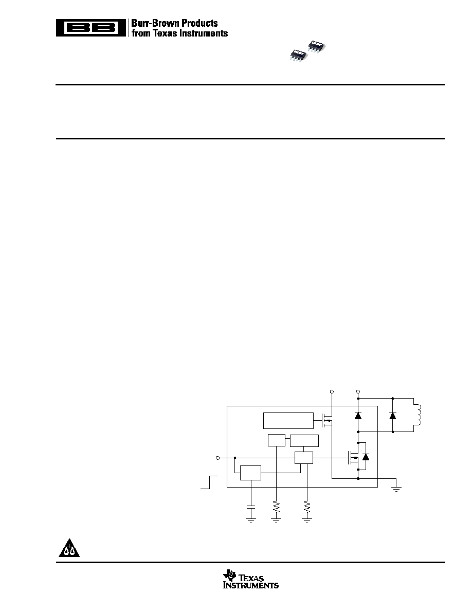
DESCRIPTION
The DRV103 is a low-side DMOS power switch employing
a pulse-width modulated (PWM) output. Its rugged design is
optimized for driving electromechanical devices such as
valves, solenoids, relays, actuators, motors, and positioners.
The DRV103 is also ideal for driving thermal devices such
as heaters, coolers, and lamps. PWM operation conserves
power and reduces heat rise, resulting in higher reliability. In
addition, adjustable PWM allows fine control of the power
delivered to the load. DC-to-PWM output delay time and
oscillator frequency are also externally adjustable.
The DRV103 can be set to provide a strong initial closure,
automatically switching to a "soft" hold mode for power
savings. A resistor, analog voltage, or Digital-to-Analog
(D/A) converter can control the duty cycle. An output OK flag
indicates when thermal shutdown or over current occurs.
Two packages provide a choice of output current:
1.5A (SO-8) or 3A (PowerPADTM SO-8 with exposed metal
heat sink).
The DRV103 is specified for ≠40
∞
C to +85
∞
C.
Delay
Adj
C
D
R
PWM
Input
On
Off
Thermal Shutdown
Over Current
Status OK
Flag
Load
+V
S
Oscillator
V
REF
PWM
GND
OUT
Flyback
Diode
DMOS
DMOS
ESD
Osc Freq
Adj
Duty Cycle
Adj
R
FREQ
Delay
DRV103
DRV103
SBVS029A ≠ JUNE 2001
www.ti.com
Copyright © 2001, Texas Instruments Incorporated
Please be aware that an important notice concerning availability, standard warranty, and use in critical applications of
Texas Instruments semiconductor products and disclaimers thereto appears at the end of this data sheet.
PowerPAD is a trademark of Texas Instruments.
DRV1
03
DRV1
03

DRV103
2
SBVS029A
PACKAGE
SPECIFIED
DRAWING
TEMPERATURE
PACKAGE
ORDERING
TRANSPORT
PRODUCT
PACKAGE
NUMBER
RANGE
MARKING
NUMBER
(1)
MEDIA
DRV103U
SO-8
182
≠40
∞
C to +85
∞
C
DRV103U
DRV103U
Rails
"
"
"
"
"
DRV103U/2K5
Tape and Reel
DRV103H
PowerPADTM SO-8
DDA
≠40
∞
C to +85
∞
C
DRV103H
DRV103H
Rails
"
"
"
"
"
DRV103H/2K5
Tape and Reel
NOTES: (1) Models with a slash (/) are available only in Tape and Reel in the quantities indicated (e.g., /2K5 indicates 2500 devices per reel). Ordering 2500
pieces of "DRV103U/2K5" will get a single 2500-piece Tape and Reel.
Supply Voltage, V
S
(2)
......................................................................... +40V
Input Voltage .................................................................. ≠0.2V to +5.5V
(3)
PWM Adjust Input .......................................................... ≠0.2V to +5.5V
(3)
Delay Adjust Input .......................................................... ≠0.2V to +5.5V
(3)
Frequency Adjust Input .................................................. ≠0.2V to +5.5V
(3)
Status OK Flag and OUT .................................................... ≠0.2V to V
S
(4)
Operating Temperature Range ...................................... ≠55
∞
C to +125
∞
C
Storage Temperature Range ......................................... ≠65
∞
C to +150
∞
C
Junction Temperature .................................................................... +150
∞
C
Lead Temperature (soldering, 10s) ............................................... +300
∞
C
NOTES: (1) Stresses above these ratings may cause permanent damage.
Exposure to absolute maximum conditions for extended periods may de-
grade device reliability. (2) See Bypassing section for discussion about
operating near maximum supply voltage. (3) Higher voltage may be applied
if current is limited to 2mA. (4) The Status OK Flag will internally current limit
at about 10mA.
ABSOLUTE MAXIMUM RATINGS
(1)
ELECTROSTATIC
DISCHARGE SENSITIVITY
This integrated circuit can be damaged by ESD. Texas Instru-
ments recommends that all integrated circuits be handled with
appropriate precautions. Failure to observe proper handling
and installation procedures can cause damage.
ESD damage can range from subtle performance degradation
to complete device failure. Precision integrated circuits may
be more susceptible to damage because very small parametric
changes could cause the device not to meet its published
specifications.
PACKAGE/ORDERING INFORMATION

DRV103
3
SBVS029A
ELECTRICAL CHARACTERISTICS
At T
C
= +25
∞
C, V
S
= +24V, Load = 100
, and 4.99k
"OK Flag" pullup to +5V, Delay Adj Capacitor = 100pF to Ground, Freq Adj Resistor = 205k
to Ground,
Duty Cycle Adj Resistor = 137k
to Ground, unless otherwise noted.
DRV103U, H
PARAMETER
CONDITIONS
MIN
TYP
MAX
UNITS
OUTPUT
Output Current
(1)
SO-8 Package (U)
1.5
A
PowerPADTM SO-8 Package (H)
3
A
Output Saturation Voltage, Source
I
O
= 1A
+0.4
+0.6
V
I
O
= 0.1A
+0.05
+0.07
V
Current Limit
(2), (10)
3
3.5
4.2
A
Leakage Current
DMOS Output Off, V
O
= +32V
±
1
±
10
µ
A
DIGITAL CONTROL INPUT
(3)
V
CTR
Low (output disabled)
0
+1.2
V
V
CTR
High (output enabled)
+2.2
+5.5
V
I
CTR
Low (output disabled)
V
CTR
= 0V
0.01
1
µ
A
I
CTR
High (output enabled)
V
CTR
= +5.5V
120
150
µ
A
Propagation Delay
On-to-Off and Off-to-On
1
µ
s
DELAY TO PWM
(4)
DC to PWM Mode
Delay Equation
(5)
See Note (6)
s
Delay Time
C
D
= 0.1
µ
F
90
110
140
ms
Minimum Delay Time
(7)
C
D
= 0
18
µ
s
DUTY CYCLE ADJUST
Duty Cycle Range
10 to 90
%
Duty Cycle Accuracy
50% Duty Cycle, 25kHz
±
2
%
vs Supply Voltage
50% Duty Cycle, V
S
= V
O
= +8V to +32V
±
2
%
Nonlinearity
(8)
10% to 90% Duty Cycle
1
% FSR
DYNAMIC RESPONSE
Output Voltage Rise Time
V
O
= 10% to 90% of V
S
0.2
2
µ
s
Output Voltage Fall Time
V
O
= 90% to 10% of V
S
0.2
2
µ
s
Oscillator Frequency Range
External Adjust
0.5 to 100
kHz
Oscillator Frequency
R
OSC
= 205k
20
25
30
kHz
OK FLAG
Normal Operation
20k
Pull-Up to +5V
+4.5
5.0
V
Fault
(90)
Sinking 1mA
+0.22
+0.4
V
Sink Current
V
OKFLAG
= 0.4V
2
mA
Over-Current Flag: Set
5
µ
s
THERMAL SHUTDOWN
Junction Temperature
Shutdown
+160
∞
C
Reset from Shutdown
+140
∞
C
POWER SUPPLY
Specified Operating Voltage
+24
V
Operating Voltage Range
+8
+32
V
Quiescent Current
I
O
= 0
0.4
0.8
mA
TEMPERATURE RANGE
Specified Range
≠40
+85
∞
C
Operating Range
≠55
+125
∞
C
Storage Range
≠65
+150
∞
C
Thermal Resistance,
JA
SO-8 (U)
1in
2
0.5oz. Copper on PCB
150
∞
C/W
PowerPADTM SO-8 (H)
(10)
1in
2
0.5oz. Copper on PCB
68
∞
C/W
NOTES: (1) Output current is limited by internal current limit and by DRV103 power dissipation. (2) Output current resets to zero when current limit is reached.
(3) Logic High enables output (normal operation). (4) Constant DC output to PWM (Pulse-Width Modulated) time. (5) Maximum delay is determined by an external
capacitor. Pulling the Delay Adjust Pin LOW corresponds to an infinite (continuous) delay. (6) Delay to PWM
C
D
∑ 10
6
(C
D
in
F ∑ 1.1). (7) Connecting the Delay Adjust Pin to +5V reduces delay time to less than 1
µ
s. (8) V
IN
at pin 3 to percent of duty cycle at pin 6. (9) OK Flag LOW indicates
fault from over-temperature or over-current conditions. (10) PowerPADTM SO-8 (H) package has highest continuous current (2A) because the chip operates at a
lower junction temperature when underside metal tab is connected to a heat sink or heat spreader.
JA
= 68
∞
C/W measured on DRV103 demo board;
JA
= 58
∞
C/W measured on JEDEC standard test board. H package
JC
= 16.7
∞
C/W.
DRV103
4
SBVS029A
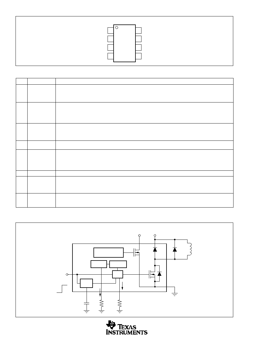
PIN #
NAME
DESCRIPTION
Pin 1
Duty Cycle Adjust
Internally, this pin connects to the input of a comparator and a (2.75 x I
REF
) current source from V
S
. The voltage at this node linearly
sets the duty cycle. Duty cycle can be programmed with a resistor, analog voltage, or the voltage output of a D/A converter. The
active voltage range is from 1.3V to 3.9V to facilitate the use of single-supply control electronics. At 3.56V, output duty cycle is near
90%. At 1.5V, output duty cycle is near 10%.
Pin 2
Delay Adjust
This pin sets the duration of the initial 100% duty cycle before the output goes into PWM mode. Leaving this pin floating results
in a delay of approximately 18
µ
s, which is internally limited by parasitic capacitance. Minimum delay may be reduced to less than
1
µ
s by tying the pin to 5V. This pin connects internally to a 3
µ
A current source from V
S
and to a 2.6V threshold comparator. When
the pin voltage is below 2.6V, the output device is 100% ON. The PWM oscillator is not synchronized to the Input (pin 1), so the
duration of the first pulse may be any portion of the programmed duty cycle.
Pin 3
Oscillator
PWM frequency is adjustable. A resistor to ground sets the current I
REF
and the internal PWM oscillator frequency. A range of 500Hz
Frequency Adjust
to 100kHz can be achieved with practical resistor values. Although oscillator frequency operation below 500Hz is possible, resistors
higher than 10M will be required. The pin then becomes a very high impedance node and is, therefore, sensitive to noise pickup
and PCB leakage currents.
Pin 4
GND
This pin must be connected to system ground for the DRV103 to function. It carries the 0.4mA quiescent current plus the full load
current when the power DMOS transistor is switched on.
Pin 5
OUT
The output is the drain of a power DMOS transistor with its source connected to ground. Its low on-resistance (0.5
typ) assures
low power dissipation in the DRV103. Gate drive to the power device is controlled to provide a slew-rate limited rise and fall time.
This reduces radiated RFI/EMI noise. A flyback diode is needed with inductive loads to conduct the load current during the off
cycle. The external diode should be selected for low forward voltage and low storage time. The internal clamp diode (an ESD
protection diode) provides some degree of back-EMF protection but it should not be used as a flyback diode.
Pin 6
+V
S
This is the power supply pin. Operating range is +8V to +32V. +V
S
must be
the supply voltage to the load.
Pin 7
Status OK Flag
Normally HIGH (active LOW), a Flag LOW signals either an over-temperature or over-current fault. The over-current flag (Status
OK) is LOW only when the output is ON (constant DC output or the "ON" portion of PWM mode). A thermal fault (thermal shutdown)
occurs when the die surface reaches approximately 160
∞
C and latches until the die cools to 140
∞
C. This output requires a pull-
up resistor and it can typically sink 2mA, sufficient to drive a low-current LED. Sink current is internally limited at 10mA typical.
Pin 8
Input
The input is compatible with standard TTL levels. The device output becomes enabled when the input voltage is driven above the
typical switching threshold, 1.7V. Below this level, the output is disabled. Input current is typically 10nA when driven HIGH and 10nA
with the input LOW. The input should not be directly connected to the power supply (V
S
) or damage will occur.
PIN DESCRIPTIONS
LOGIC BLOCK DIAGRAM
PIN CONFIGURATION
Top View
Duty Cycle Adj
Delay Adj
Osc Freq Adj
GND
Input
Status OK Flag
+V
S
OUT
1
2
3
4
8
7
6
5
Delay
Adj
C
D
R
PWM
Input
On
Off
Thermal Shutdown
Over Current
Status OK
Flag
Load
+V
S
Oscillator
1.3V V
REF
PWM
GND
OUT
Flyback
Diode
DMOS
DMOS
ESD
Osc Freq
Adj
Duty Cycle
Adj
2.75 ∑ I
REF
R
FREQ
Delay
DRV103
I
REF
SO
DRV103
5
SBVS029A
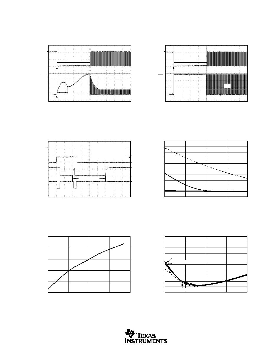
TYPICAL CHARACTERISTICS
At T
C
= +25
∞
C and V
S
= +24V, unless otherwise noted.
V
OUT
& I
OUT
WAVEFORMS
SOLENOID LOAD
On
On
Off
I
AVG
PWM Mode
Delay
Pull-In
3
2
1
0
I
OUT
(A)
50
Time (ms)
100
0
+V
S
0
0
+V
S
R
L
V
OUT
& I
OUT
WAVEFORMS
RESISTIVE LOAD
On
Off
I
AVG
PWM Mode
Delay
3
2
1
0
I
OUT
(A)
50
Time (ms)
100
0
+V
S
0
0
+V
S
R
L
CURRENT LIMIT SHUTDOWN WAVEFORMS
On
OK
OK
OK
OK
Off
Off
F
PWM
= 25kHz
DC = 50%
Delay = 150
µ
s
Reset Period = 1/F
PWM
5
0
24
0
24
0
V
IN
(V)
V
OUT
(V)
50
Time (
µ
s)
100
0
V
IN
V
OUT
I
O
= 0A
I
O
= 3.5A
OK
Status
OK
Flag
Reset Period
5.0
4.5
4.0
3.5
3.0
2.5
2.0
1.5
1.0
0.5
0
≠10
≠60
I
Q
(mA)
40
90
140
QUIESCENT CURRENT
vs JUNCTION TEMPERATURE
Temperature (
∞
C)
32V
8V to 24V
40V (Absolute Maximum)
3.8
3.7
3.6
3.5
3.4
3.3
≠10
≠60
Current (A)
40
90
140
CURRENT LIMIT
vs JUNCTION TEMPERATURE
Temperature (
∞
C)
150
145
140
135
130
125
120
115
110
105
100
≠10
≠60
Delay (ms)
40
90
140
DELAY vs JUNCTION TEMPERATURE
Temperature (
∞
C)
C
D
= 0.1
µ
F
+V
S
= 8V
+V
S
= 30V
+V
S
= 24V
+V
S
= 40V (Absolute Maximum)