 | –≠–ª–µ–∫—Ç—Ä–æ–Ω–Ω—ã–π –∫–æ–º–ø–æ–Ω–µ–Ω—Ç: DRV1100 | –°–∫–∞—á–∞—Ç—å:  PDF PDF  ZIP ZIP |

DRV1100
Æ
In+
In≠
Out+
+5V
G = 3V/V
DRV1100
Patent
Pending
GND
Out≠
4
4
Protection
1:4
Transformer
135
HIGH POWER DIFFERENTIAL DRIVER AMPLIFIER
OPA658
DRV1100
DRV1100
International Airport Industrial Park ∑ Mailing Address: PO Box 11400, Tucson, AZ 85734 ∑ Street Address: 6730 S. Tucson Blvd., Tucson, AZ 85706 ∑ Tel: (520) 746-1111 ∑ Twx: 910-952-1111
Internet: http://www.burr-brown.com/ ∑ FAXLine: (800) 548-6133 (US/Canada Only) ∑ Cable: BBRCORP ∑ Telex: 066-6491 ∑ FAX: (520) 889-1510 ∑ Immediate Product Info: (800) 548-6132
DESCRIPTION
The DRV1100 is fixed gain differential line driver
designed for very low harmonic distortion at the high
powers required of xDSL line interface standards.
Operating on a single +5V supply, it can deliver
230mA peak output current and 9.5Vp-p differential
output voltage swing. This high output power on a
single +5V supply makes the DRV1100 an excellent
choice for the xDSL applications that require up to
17dBm power onto the line with high crest factors.
The DRV1100 is available in both 8-pin plastic DIP
and SO-8 packages.
FEATURES
q
HIGH OUTPUT CURRENT: 230mA
q
SINGLE SUPPLY OPERATION: 5V
q
5MHz BANDWIDTH: 6Vp-p into 15
q
VERY LOW THD AT HIGH POWER:
≠72dBc at 6Vp-p, 100kHz, 100
q
LOW QUIESCENT CURRENT: 11mA
q
FIXED DIFFERENTIAL GAIN: 3V/V
APPLICATIONS
q
xDSL TWISTED PAIR LINE DRIVER
q
COMMUNICATIONS LINE DRIVER
q
TRANSFORMER DRIVER
q
SOLENOID DRIVER
q
HIGH POWER AUDIO DRIVER
q
CRT YOKE DRIVER
©
1996 Burr-Brown Corporation
PDS-1354
Printed in U.S.A. December, 1996
SBWS004
2
Æ
DRV1100
DRV1100P, U
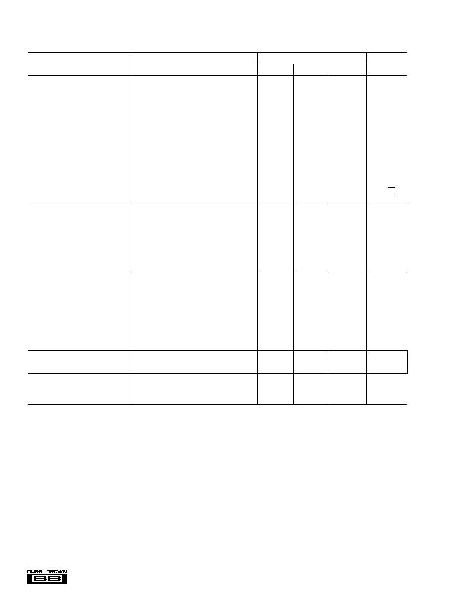
PARAMETER
CONDITIONS
MIN
TYP
MAX
UNITS
AC PERFORMANCE
≠3dB Bandwidth
R
L
= 15
, V
O
= 1Vp-p
8
MHz
R
L
100
, V
O
= 1Vp-p
11
MHz
R
L
= 15
, V
O
= 6Vp-p
5
MHz
R
L
100
, V
O
= 6Vp-p
6
MHz
Differential Slew Rate
R
L
= 100
, V
O
= 6Vp-p
80
V/
µ
s
Step Response Delay
(1)
V
O
= 1Vp-p
25
ns
Settling Time to 1%, Step Input
V
O
= 1Vp-p, R
L
= 100
0.25
µ
s
Settling Time to 1%, Step Input
V
O
= 6Vp-p, R
L
= 100
0.3
µ
s
Settling Time to 0.1%, Step Input
V
O
= 1Vp-p, R
L
= 100
0.8
µ
s
Settling Time to 0.1%, Step Input
V
O
= 6Vp-p, R
L
= 100
1.1
µ
s
THD, Total Harmonic Distortion
(2)
f = 10kHz
R
L
= 100
, V
O
= 6Vp-p
≠85
dBc
f = 10kHz
R
L
= 15
, V
O
= 6Vp-p
≠66
≠76
dBc
f = 100kHz
R
L
= 100
, V
O
= 6Vp-p
≠72
dBc
f = 100kHz
R
L
= 15
, V
O
= 6Vp-p
≠65
dBc
Input Voltage Noise
f = 100kHz
30
nV/
Hz
Input Current Noise
f = 100kHz
0.5
fA/
Hz
INPUT CHARACTERISTICS
Differential Input Resistance
10
11
Differential Input Capacitance
1
pF
Common-Mode Input Resistance
10
11
Common-Mode Input Capacitance
6
pF
Input Offset Voltage
5
mV
Input Bias Current
1
pA
Common-Mode Rejection Ratio
Input Referred
62
dB
Power Supply Rejection Ratio
Input Referred
60
76
dB
Input Common-Mode Voltage Range
(3)
0.5
V
DD
≠0.5
V
OUTPUT CHARACTERISTICS
Differential Output Offset, RTO
10
25
mV
Differential Output Offset Drift, RTO
≠40
∞
C to +85
∞
C
30
µ
V/
∞
C
Differential Output Resistance
0.16
Peak Current (Continuous)
R
L
= 15
200
230
mA
Differential Output Voltage Swing
R
L
= 1k
9.6
Vp-p
R
L
= 100
8.5
9.5
Vp-p
R
L
= 15
6.0
6.6
Vp-p
Output Voltage Swing, Each Side
R
L
= 1k
0.125
4.875
V
Gain
Fixed Gain, Differential
3
V/V
Gain Error
±
0.25
dB
POWER SUPPLY
Operating Voltage Range
+4.5
+5.0
+5.5
V
Quiescent Current
V
DD
= 5.0V
+11
+16
mA
TEMPERATURE RANGE
≠40
+85
∞
C
Thermal Resistance,
JA
DRV1100P
8-Pin DIP
100
∞
C/W
DRV1100U
8-Pin SO-8
125
∞
C/W
NOTES: (1) Time from 50% point of input step to 50% point of output step. (2) Measurement Bandwidth = 500kHz. (3) Output common-mode voltage follows input
common-mode voltage; therefore, if input V
CM
= V
DD
/2, then output V
CM
= V
DD
/2.
SPECIFICATIONS
At V
DD
= +5.0V, V
CM
= V
DD
/2, T
A
= 25
∞
C, unless otherwise specified.
The information provided herein is believed to be reliable; however, BURR-BROWN assumes no responsibility for inaccuracies or omissions. BURR-BROWN
assumes no responsibility for the use of this information, and all use of such information shall be entirely at the user's own risk. Prices and specifications are subject
to change without notice. No patent rights or licenses to any of the circuits described herein are implied or granted to any third party. BURR-BROWN does not
authorize or warrant any BURR-BROWN product for use in life support devices and/or systems.

3
Æ
DRV1100
PIN CONFIGURATIONS
Top View
Analog Inputs: Current ..............................................
±
100mA, Momentary
±
10mA, Continuous
Voltage ....................................... GND ≠0.3V to V
DD
+0.2V
Analog Outputs Short Circuit to Ground (+25
∞
C) ..................... Momentary
Analog Outputs Short Circuit to V
DD
(+25
∞
C) ........................... Momentary
V
DD
to GND .............................................................................. ≠0.3V to 6V
Junction Temperature ................................................................... +150
∞
C
Storage Temperature Range .......................................... ≠40
∞
C to +125
∞
C
Lead Temperature (soldering, 3s) ................................................. +260
∞
C
Power Dissipation .............................. (See Thermal/Analysis Discussion)
ABSOLUTE MAXIMUM RATINGS
In+
2
6
7
4
1
3
5
8
In≠
Out+
+5V
GND
Out≠
PACKAGE/ORDERING INFORMATION
PACKAGE DRAWING
PRODUCT
PACKAGE
NUMBER
(1)
DRV1100P
8-Pin PDIP
006
DRV1100U
8-Lead SO-8
182
NOTE: (1) For detailed drawing and dimension table, please see end of data
sheet, or Appendix C of Burr-Brown IC Data Book.
ELECTROSTATIC
DISCHARGE SENSITIVITY
This integrated circuit can be damaged by ESD. Burr-Brown
recommends that all integrated circuits be handled with
appropriate precautions. Failure to observe proper handling
and installation procedures can cause damage.
ESD damage can range from subtle performance degradation
to complete device failure. Precision integrated circuits may
be more susceptible to damage because very small parametric
changes could cause the device not to meet its published
specifications.
GND
In+
In≠
GND
Out≠
V
DD
(+5V)
V
DD
(+5V)
Out+
1
2
3
4
8
7
6
5
4
Æ
DRV1100
TYPICAL PERFORMANCE CURVES
At V
DD
= +5.0V, V
CM
= V
DD
/2, T
A
= 25
∞
C, unless otherwise specified.
≠40
≠45
≠50
≠55
≠60
≠65
≠70
≠75
≠80
100K
SMALL SIGNAL 2ND HARMONIC DISTORTION
2nd Harmonic (dB)
Frequency (Hz)
1M
10M
R
L
= 15
V
O
= 1Vp-p
R
L
= 100
≠40
≠45
≠50
≠55
≠60
≠65
≠70
≠75
≠80
100K
SMALL SIGNAL 3RD HARMONIC DISTORTION
3rd Harmonic (dB)
Frequency (Hz)
1M
10M
V
O
= 1Vp-p
R
L
= 100
R
L
= 15
≠40
≠45
≠50
≠55
≠60
≠65
≠70
≠75
≠80
100K
LARGE SIGNAL 2ND HARMONIC DISTORTION
2nd Harmonic (dB)
Frequency (Hz)
1M
10M
R
L
= 15
V
O
= 6Vp-p
R
L
= 100
≠40
≠45
≠50
≠55
≠60
≠65
≠70
≠75
≠80
100K
LARGE SIGNAL 3RD HARMONIC DISTORTION
3rd Harmonic (dB)
Frequency (Hz)
1M
10M
V
O
= 6Vp-p
R
L
= 100
R
L
= 15
9.5
8.5
7.5
6.5
5.5
4.5
3.5
2.5
1.5
10K
100K
SMALL SIGNAL FREQUENCY RESPONSE
Differential Gain (dB)
Frequency (Hz)
1M
10M
R
L
= 1k
R
L
= 100
R
L
= 15
V
O
= 1Vp-p
9.5
8.5
7.5
6.5
5.5
4.5
3.5
2.5
1.5
10K
100K
LARGE SIGNAL FREQUENCY RESPONSE
Differential Gain (dB)
Frequency (Hz)
1M
10M
R
L
= 1k
R
L
= 100
R
L
= 15
V
O
= 6Vp-p

5
Æ
DRV1100
TYPICAL PERFORMANCE CURVES
(CONT)
At V
DD
= +5.0V, V
CM
= V
DD
/2, T
A
= 25
∞
C, unless otherwise specified.
≠40
≠50
≠60
≠70
≠80
≠90
1
2
3
4
10kHz THD
THD (dBc)
Differential Output Voltage (Vp-p)
5
6
7
8 9 10
R
L
= 15
R
L
= 100
R
L
= 1k
≠40
≠50
≠60
≠70
≠80
≠90
1
2
3
4
100kHz THD
THD (dBc)
Differential Output Voltage (Vp-p)
5
6
7
8 9 10
R
L
= 15
R
L
= 100
R
L
= 1k
+0.5V
0
≠0.5V
SMALL SIGNAL STEP RESPONSE
Differential Voltage (125mV/div)
Time (50ns/div)
Output
Input
R
L
= 100
+3V
0
≠3V
LARGE SIGNAL STEP RESPONSE
Differential Voltage (750mV/div)
Time (50ns/div)
Output
Input
R
L
= 100
12
10
8
6
4
2
0
MAXIMUM V
O
vs SUPPLY VOLTAGE
Differential Output Voltage (Vp-p)
Supply Voltage (V
DD
)
4.5
4.75
5
5.25
5.5
R
L
= 100
R
L
= 1k
R
L
= 15
10
9
8
7
6
5
4
3
2
1
0
10K
1K
100K
LARGE SIGNAL OPERATING RANGE
Differential Output Swing (Vp-p)
Frequency (Hz)
1M
10M
R
L
= 15
R
L
= 1k
R
L
= 100
1% THD