 | –≠–ª–µ–∫—Ç—Ä–æ–Ω–Ω—ã–π –∫–æ–º–ø–æ–Ω–µ–Ω—Ç: GC4014 | –°–∫–∞—á–∞—Ç—å:  PDF PDF  ZIP ZIP |

SLWS132
GC4014
QUAD RECEIVER CHIP
DATASHEET
April 27, 1999
Rev 0.5
This datasheet contains information which may be changed at any time without notice.

GRAYCHIP, INC.
- i -
APRIL 27, 1999
GC4014 QUAD RECEIVER CHIP
DATA SHEET REV 0.5
This document contains information which may be changed at any time without notice
REVISION HISTORY
Revision
Date
Description
0.0
1 Dec. 1997
Original
0.1
14 Jan 1998
Page iii, added mask revision table to list of tables
Pages 8, last line, added non-symmetry mode errata
Page 10, footnote, changed "1 milliseconds" to "10 microseconds".
Page 11, modified Figure 10 (c)
Page 12, first line Section 3.7, changed "output" to "input".
Page 18, address 1, bit 6, added non-symmetry errata
Page 19, address 4, bits 4-7, corrected bit assignments
Pages 20-21, corrected address numbering for blanking and flush registers
Page 22, address 12, bits 0,1, changed "12 LSBs" to "14 LSBs".
Page 24, address 16, added mask revision table.
Throughout, corrected table and figure reference
0.2
21 Jan 1998
Page 30, Changed data setup time from 4 to 2 ns.
Page 8, 18 Non-symmetry mode works for parts marked with all mask codes
except 55532B
Page 24, Changed Table 5 to add mask code 55532C
Page 28, Table 7 min and max recommended Vcc changed to 3.1 to 3.5 volts.
Page 28, Table 7 max junction temperature changed to 125C.
0.3
5 Feb 1998
Page 38, Changed 800 to 8000 in Table 17.
Page 38, Changed E5 to EA in note 1, Table 16.
Page 37, Checksum for test4 changed to D2.
0.4
23 Apr 1999
Page 38, Changed CS to CE in the control interface timing description, Table 10
Pages 9,19, Changed GAIN equation from
"NARROW*1.97"
to
"NARROW*0.97 + 1"
Page 28, Table 7, Changed max Vup voltage to 5.5v.
Page 39, New gain application note.
Pages 5, 25, Positive frequency to downconvert.
Pages 36, 37, changed 26 -> 2A for address 00
Page 29, Table 9, changed V
IH
for CK, CK2X to 2.4V from 2.0V.
Page 29, Table 9, changed I
OH/L
to +/- 4mA from 2.0mA
Page 30, F
CK
changed to 64MHz, clock to output changed to 20ns.
0.5
27 Apr 1999
Pages 9,19,33,35,39, changed gain equation G/64 -> G/32
0.6
Pages 6, 38 changed 55 to 56 in gain equations.

GRAYCHIP, INC.
- ii -
APRIL 27, 1999
GC4014 QUAD RECEIVER CHIP
DATA SHEET REV 0.5
This document contains information which may be changed at any time without notice
CONTACTING GRAYCHIP
CORPORATE OFFICES:
GRAYCHIP, Inc.
2185 Park Blvd.
Palo Alto, CA 94306
PHONE:
(650) 323-2955
FAX:
(650) 323-0206
WEB PAGE:
www.graychip.com
E-MAIL:
sales@graychip.com
tech-support@graychip.com

GRAYCHIP,INC.
- iii -
APRIL 27, 1999
GC4014 QUAD RECEIVER CHIP
DATA SHEET REV 0.5
This document contains information which may be changed at any time without notice
1.0
KEY FEATURES .........................................................................................................................1
2.0
BLOCK DIAGRAM .....................................................................................................................1
3.0
FUNCTIONAL DESCRIPTION ...................................................................................................2
3.1
CONTROL INTERFACE ....................................................................................................................... 2
3.2
INPUT FORMAT ................................................................................................................................... 3
3.3
THE DOWN CONVERTERS ................................................................................................................ 4
3.4
FINAL GAIN ADJUSTMENT ................................................................................................................ 9
3.5
SUMMATION MODES ......................................................................................................................... 9
3.6
OUTPUT MODES ............................................................................................................................... 10
3.7
CLOCKING ......................................................................................................................................... 12
3.8
POWER DOWN MODES ................................................................................................................... 12
3.9
SYNCHRONIZATION ......................................................................................................................... 12
3.10
DATA LATENCY ................................................................................................................................ 13
3.11
DIAGNOSTICS ................................................................................................................................... 13
4.0
PACKAGING .............................................................................................................................14
5.0
CONTROL REGISTERS............................................................................................................16
5.1
SYNC MODE REGISTER ................................................................................................................... 17
5.2
DECIMATION MODE REGISTER....................................................................................................... 18
5.3
CIC DECIMATION REGISTERS ......................................................................................................... 18
5.4
SCALE CONTROL REGISTER........................................................................................................... 19
5.5
CHANNEL GAIN REGISTER .............................................................................................................. 19
5.6
OUTPUT FORMAT REGISTER .......................................................................................................... 20
5.7
OUTPUT MODE REGISTER............................................................................................................... 20
5.8
BLANKING CONTROL REGISTER .................................................................................................... 20
5.9
CHANNEL FLUSH CONTROL REGISTER......................................................................................... 21
5.10
COUNTER MODE REGISTERS ......................................................................................................... 21
5.11
TEST MODE REGISTER .................................................................................................................... 22
5.12
PAGE MAP REGISTER ...................................................................................................................... 22
5.13
STATUS CONTROL REGISTER ........................................................................................................ 23
5.14
CHECKSUM REGISTER..................................................................................................................... 23
5.15
CHANNEL OUTPUT PAGE (PAGE = 0) ............................................................................................. 24
5.16
KEEPALIVE STATUS PAGE (PAGE = 1) ........................................................................................... 24
5.17
CHANNEL CONTROL PAGES (PAGES 4, 5, 6, 7)............................................................................. 25
5.18
COEFFICIENT STORAGE PAGES (PAGES 8, 9, 10 and 11)............................................................ 27
6.0
SPECIFICATIONS .....................................................................................................................28
6.1
ABSOLUTE MAXIMUM RATINGS ...................................................................................................... 28
6.2
RECOMMENDED OPERATING CONDITIONS.................................................................................. 28
6.3
THERMAL CHARACTERISTICS ........................................................................................................ 28
6.4
DC CHARACTERISTICS .................................................................................................................... 29
6.5
AC CHARACTERISTICS..................................................................................................................... 30
7.0
APPLICATION NOTES..............................................................................................................31
7.1
POWER AND GROUND CONNECTIONS.......................................................................................... 31
7.2
STATIC SENSITIVE DEVICE.............................................................................................................. 31
7.3
SYNCHRONIZING MULTIPLE GC4014 CHIPS ................................................................................. 31
7.4
THERMAL MANAGEMENT................................................................................................................. 31
7.5
GSM APPLICATION............................................................................................................................ 32
7.6
DAMPS APPLICATION ....................................................................................................................... 34
7.7
DIAGNOSTICS.................................................................................................................................... 36
7.8
OUTPUT TEST CONFIGURATION .................................................................................................... 38
7.9
OPTIMAL GAIN SETTINGS ................................................................................................................ 39

GRAYCHIP,INC.
-iv -
APRIL 27, 1999
GC4014 QUAD RECEIVER CHIP
DATA SHEET REV 0.5
This document contains information which may be changed at any time without notice
LIST OF FIGURES
Figure 1:
GC4014 Block Diagram .................................................................................................................. 1
Figure 2:
Control I/O Timing ........................................................................................................................... 3
Figure 3:
The Down Converter Channel......................................................................................................... 4
Figure 4:
NCO Circuit ..................................................................................................................................... 5
Figure 5:
Example NCO Spurs....................................................................................................................... 5
Figure 6:
NCO Peak Spur Scan Plot .............................................................................................................. 6
Figure 7:
Four Stage CIC Decimate by N Filter.............................................................................................. 6
Figure 8:
Combined CFIR and CIC Frequency Response ............................................................................. 7
Figure 9:
Overall CIC-CFIR-PFIR Response ................................................................................................. 8
Figure 10: Serial Output Formats ................................................................................................................... 11
Figure 11: Overall Frequency Response for GSM ......................................................................................... 32
Figure 12: Overall Frequency Response for DAMPS..................................................................................... 34
LIST OF TABLES
Table 1:
Output Summation Modes .............................................................................................................. 9
Table 2:
TDM Modes................................................................................................................................... 10
Table 3:
Latency.......................................................................................................................................... 13
Table 4:
Sync Modes .................................................................................................................................. 17
Table 5:
Mask Revision History................................................................................................................... 24
Table 6:
Absolute Maximum Ratings .......................................................................................................... 28
Table 7:
Recommended Operating Conditions ........................................................................................... 28
Table 8:
Thermal Data ................................................................................................................................ 28
Table 9:
DC Operating Conditions .............................................................................................................. 29
Table 10:
AC Characteristics (-40 To +85C Ambient, unless noted) ............................................................ 30
Table 11:
GSM Configuration........................................................................................................................ 33
Table 12:
DAMPS Configuration ................................................................................................................... 35
Table 13:
Diagnostic Test 1 Configuration .................................................................................................... 36
Table 14:
Diagnostic Test 2 Configuration .................................................................................................... 36
Table 15:
Diagnostic Test 3 Configuration .................................................................................................... 37
Table 16:
Diagnostic Test 4 Configuration .................................................................................................... 37
Table 17:
Output Test Configuration ............................................................................................................. 38
Table 18:
Test Output Sequence .................................................................................................................. 38

GRAYCHIP, INC.
- 1 -
APRIL 27, 1999
GC4014 QUAD RECEIVER CHIP
DATA SHEET REV 0.6
This document contains information which may be changed at any time without notice
GC4014 DATASHEET
2.0
BLOCK DIAGRAM
A block diagram illustrating the major functions of the chip is shown in Figure 1.
Figure 1. GC4014 Block Diagram
CLOCK DOUBLING
AND
DISTRIBUTION CIRCUIT
CK
CONTROL INTERFACE
WR
RD
A[0:4]
C[0:7]
SYNC COUNTER
AND
DIAGNOSTIC TEST
SI
SO
GENERATOR
AND FILTER
CE
SINE/
COSINE
OUTPUT
FORMAT
AND GAIN
BANDWIDTH
FILTER SELECT
DECIMATE BY 8
FORMAT
SELECT
GENERATOR
A
OUT
(BIT SERIAL)
B
OUT
(BIT SERIAL)
SINE/
COSINE
GENERATOR
OUTPUT
FORMAT
AND GAIN
TWO STAGE
DECIMATE
BY 4OR 8
GAIN
GAIN
TUNING
FREQUENCY
PHASE
OFFSET
TUNING
FREQUENCY
PHASE
OFFSET
DECIMATE
BY 8 TO 16K
FILTER
DECIMATE
BY 8 TO 16K
FILTER
A
IN
B
IN
SINE/
COSINE
OUTPUT
FORMAT
AND GAIN
GENERATOR
C
OUT
(BIT SERIAL)
D
OUT
(BIT SERIAL)
SINE/
COSINE
GENERATOR
OUTPUT
FORMAT
AND GAIN
GAIN
GAIN
TUNING
FREQUENCY
PHASE
OFFSET
TUNING
FREQUENCY
PHASE
OFFSET
DECIMATE
BY 8 TO 16K
FILTER
DECIMATE
BY 8 TO 16K
FILTER
C
IN
D
IN
(14 BITS)
(14 BITS)
(14 BITS)
(14 BITS)
CROSSBAR SWITCH
OUTPUT SUM AND MULTIPLEX
BIT-CLOCK
FRAME SYNC
READY
ACKNOWLEDGE
DIAGNOSTICS
(16 bit input mode uses the D
IN
pins for the LSB's of inputs A
IN
, B
IN
, and C
IN
)
FILTER
TWO STAGE
DECIMATE
BY 4OR 8
FILTER
TWO STAGE
DECIMATE
BY 4OR 8
FILTER
TWO STAGE
DECIMATE
BY 4OR 8
FILTER
COEFFICIENT RAMS
1.0
KEY FEATURES
∑
Input rates up to 64 MSPS
∑
Four real input down-convert channels or
Two complex input downconvert channels
∑
Independent tuning frequencies
∑
Independent phase/gain controls
∑
4 by 4 14 bit Input Crossbar switch or
3 by 4 16 bit Input Crossbar switch
∑
Decimation factors of
16 to 32,768 in the real output mode
32 to 65,536 in the complex output mode
∑
Zero padding for lower decimation factors
∑
Outputs can be either:
bit serial,
nibble serial (link port)
or memory mapped
∑
Output summing for beamforming
∑
8 to 16 bit output samples
∑
0.02 Hz tuning resolution
∑
0.14 dB gain resolution
∑
Less than 0.05 dB peak to peak passband
ripple
∑
Greater than 100 dB far image rejection
∑
Greater than 95 dB spur free dynamic range
∑
User programmable 63 tap output filter
∑
Nyquist filtering for QPSK or QAM symbol
data
∑
Meets GSM, AMPS and DAMPS Cellular
specifications
∑
Microprocessor interface for control, output,
and diagnostics
∑
Built in diagnostics
∑
Microprocessor interface will accept either
3.3 or 5 volt input levels
∑
250 mW per channel at 50 MHz, 3.3 volts
∑
100 pin thin QFP package

GRAYCHIP, INC.
- 2 -
APRIL 27, 1999
GC4014 QUAD RECEIVER CHIP
DATA SHEET REV 0.6
This document contains information which may be changed at any time without notice
3.0
FUNCTIONAL DESCRIPTION
The GC4014 quad receive chip contains four identical down-conversion circuits. Each down-convert circuit
accepts a real sample rate up to 62.5 MHz, down converts a selected carrier frequency to zero, decimates the signal
rate by a programmable factor ranging from 16 to 32768 (32 to 65,536 for complex outputs), and optionally sums it
with other down converted samples. The chip outputs the four down-converted signals, or their sum. The chip
contains a user programmable output filter which can be used to arbitrarily shape the received data's spectrum. This
filter can be used as a Nyquist receive filter for digital data transmission.
Two down-converter paths can be merged to be used as a single complex input down-conversion circuit.
The down-converters are designed to maintain over 95 dB of spur free dynamic range and over 100 dB of
out of band rejection. Each down-convert circuit accepts 16 bit inputs and produces 16 bit outputs (bit serial). The
frequencies and phase offsets of the four sine/cosine sequence generators can be independently specified, as can
the gain of each circuit. The down converters share the same bandwidth, filter coefficients and input formats. A
special mode allows the downconverters to support GSM and DAMPS blocker requirements (see Sections 7.5 and
7.6).
On chip diagnostic circuits are provided to simplify system debug and maintenance.
The chip receives configuration and control information over a microprocessor compatible bus consisting of
an 8 bit data I/O port, a 5 bit address port, a chip enable strobe, a read strobe and a write strobe. The chip's control
registers (8 bits each) are memory mapped into the 5 bit address space of the control port.
Section 7.5 Describes a typical application, including control register values and the proper sequence of
operations required to use the chip.
3.1
CONTROL INTERFACE
The chip is configured by writing control information into sixty four control registers within the chip. The
contents of these control registers and how to use them are described in Section 5. The registers are written to or
read from using the
C[0:7]
,
A[0:4]
,
CE
,
RD
and
WR
pins. Each control register has been assigned a unique address
within the chip. This interface is designed to allow the GC4014 to appear to an external processor as a memory
mapped peripheral (the pin
RD
is equivalent to a memory chip's
OE
pin).
An external processor (a microprocessor, computer, or DSP chip) can write into a register by setting
A[0:4]
to the desired register address, selecting the chip using the
CE
pin, setting
C[0:7]
to the desired value and then
pulsing
WR
low. The data will be written into the selected register when both
WR
and
CE
are low and will be held
when either signal goes high.
To read from a control register the processor must set
A[0:4]
to the desired address, select the chip with
the
CE
pin, and then set
RD
low. The chip will then drive
C[0:7]
with the contents of the selected register. After the
GRAYCHIP, INC.
- 3 -
APRIL 27, 1999
GC4014 QUAD RECEIVER CHIP
DATA SHEET REV 0.6
This document contains information which may be changed at any time without notice
processor has read the value from
C[0:7]
it should set
RD
and
CE
high. The
C[0:7]
pins are turned off (high
impedance) whenever
CE
or
RD
are high or when
WR
is low. The chip will only drive these pins when both
CE
and
RD
are low and
WR
is high.
One can also ground the
RD
pin and use the
WR
pin as a read/write direction control and use the
CE
pin
as a control I/O strobe. Figure 2 shows timing diagrams illustrating both I/O modes.
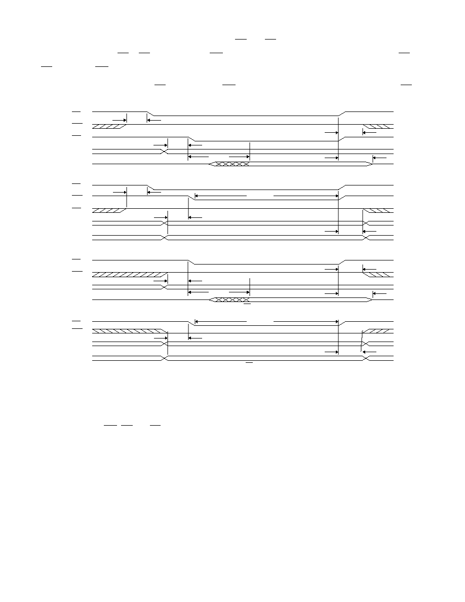
Figure 2. Control I/O Timing
The setup, hold and pulse width requirements for control read or write operations are given in
Section 6.0.
The
C
,
A
,
WR
,
RD
and
CE
pins will accept either 5 volt or 3.3 volt input levels. A separate power supply
voltage pin (
V
UP
) is provided on the chip to enable this feature.
3.2
INPUT FORMAT
Both 14 bit and 16 bit input formats are accepted. In the 14 bit mode the inputs are 14 bit samples from four
different sources. In the 16 bit mode, the inputs are 16 bit samples from three different sources. In either case, a
crossbar switch allows the user to route any input to any down-converter channel. The input samples are normally
clocked into the chip at the clock rate, i.e., the input sample rate is equal to the clock rate. Input rates lower than the
clock rate can be accepted by using the zero pad mode. The zero pad mode will insert up to 15 zeroes between
CE
WR
RD
C[0-7]
A[0-5]
t
CSU
t
CDLY
t
CSU
t
CZ
READ CYCLE- NORMAL MODE
CE
WR
RD
C[0-7]
A[0-5]
t
CSU
t
CSPW
t
CSU
t
CHD
WRITE CYCLE- NORMAL MODE
WR
CE
C[0-7]
A[0-5]
t
CDLY
t
CSU
t
CZ
t
CHD
t
CHD
CE
WR
C[0-7]
A[0-5]
t
CSPW
t
CSU
t
CHD
READ CYCLE- RD HELD LOW
WRITE CYCLE- RD HELD LOW

GRAYCHIP, INC.
- 4 -
APRIL 27, 1999
GC4014 QUAD RECEIVER CHIP
DATA SHEET REV 0.6
This document contains information which may be changed at any time without notice
each input sample, allowing input data rates down to 1/16th the clock rate. Zero padding also lowers the effective
decimation ratio. For example, the minimum decimation is normally factor of 32. If the input data rate is 5 MSPS and
the chip can be clocked at 40 MHz, then the zero pad function can be used to pad the 5 MSPS input data up by a
factor of 8 to 40 MSPS. The minimum decimation of 32, once the zero padding is done, becomes a minimum
decimation of 4 relative to the original 5 MSPS data.
3.3
THE DOWN CONVERTERS
Each down converter uses an NCO and mixer to quadrature down convert a signal to baseband and then
uses a 4 stage CIC
1
filter and a two-stage decimate by 4 or 8 filter to lowpass filter and to isolate the desired signal.
A block diagram of each filter is shown below:
Figure 3. The Down Converter Channel
The CIC filter reduces the sample rate by a programmable factor ranging from 8 to 16,384. The CIC outputs
are followed by a coarse gain stage and then followed by a two stage decimate by 4 or 8 filter. The coarse gain
circuit allows the user to boost the gain of weak signals up to 42 dB in 6 dB steps. The first stage of the two stage
filter is a compensating 21 tap decimate by 2 filter (CFIR) with a choice of two sets of fixed tap weights. The first set
is designed to be flat from -0.5F
S
to +0.5F
S
, where F
S
is the output sample rate, and to reject out of band energy by
at least 80dB. The second set has a narrower output passband (-0.25F
S
to +0.25F
S
), but more out of band rejection.
The second set is ideal for systems such as GSM, which require more far band rejection (>97 dB), but with relaxed
adjacent band rejection. The second stage is a 63 tap decimate by 2 or 4 programmable filter (PFIR) with either
internal or user supplied tap weights. The internal filter is designed to be flat from -0.4F
S
to +0.4F
S
of the output
sample rate and to reject out of band energy by at least 85 dB. The user can also design and download their own
final filter to customize the channel's spectral response. Typical uses of the programmable filter include matched
(root-raised cosine) filtering, or filtering to generate oversampled outputs with greater out of band rejection. The 63
tap symmetrical filter is downloaded into the chip as 32 words, 16 bits each. The programmable PFIR coefficients
must be used to bandlimit the output in the decimate by 4 mode.
1. Hogenauer, Eugene B., An Economical Class of Digital Filters for Decimation and Interpolation, IEEE transactions on Acoustics,
Speech and Signal Processing, April 1981.
NCO
SCALE and
N
CIC FILTER
TUNING
FREQUENCY
PHASE
OFFSET
SHIFT DOWN
BIG_SCALE
NARROW
CFIR FILTER
FILTER_SELEC
T
PFIR FILTER
DECIMATE BY
8 TO 16K
DECIMATE BY 2
DECIMATE BY
COARSE
COARSE
GAIN
IN
REAL
G
FINAL
GAIN
TO
OUTPUT
FORMATTER
Q
I
2 OR 4
DEC_BY_4
GRAYCHIP, INC.
- 5 -
APRIL 27, 1999
GC4014 QUAD RECEIVER CHIP
DATA SHEET REV 0.6
This document contains information which may be changed at any time without notice
The PFIR will also, if desired, convert the complex output data to real. The complex to real conversion also
doubles the output sample rate so that the PFIR decimation is 1 or 2 in the real mode.
The PFIR filter is followed by a gain and output format circuit. The gain circuit allows the user to add an
additional 18 dB of gain in 0.14 dB steps. The output format circuit can also delete every other sample without
filtering. Anti-aliasing filtering must have already been performed (in the second stage filter). This is useful to achieve
deeper far-band rejection since the stopband performance of the CIC filter is a function of the decimation that follows
it.
3.3.1
The Numerically Controlled Oscillator (NCO)
The tuning frequency of each down converter is specified as a 32 bit word and the phase offset is specified
as a 16 bit word. The NCOs can be synchronized with NCOs on other chips. This allows multiple down converter
outputs to be coherently combined, each with a unique phase and amplitude. A block diagram of the NCO circuit is
shown in Figure 4.
Figure 4. NCO Circuit
The tuning frequency is set to FREQ according to the formula FREQ = 2
32
F/F
CK
, where F is the desired
tuning frequency and F
CK
is the chip's clock rate. The 16 bit phase offset setting is PHASE = 2
16
P/2
, where P is
the desired phase in radians ranging between 0 and 2
. Note that a positive tuning frequency is used to
downconvert the signal. A negative tuning frequency can be used to upconvert the negative image of a real signal
(inverting the spectrum).
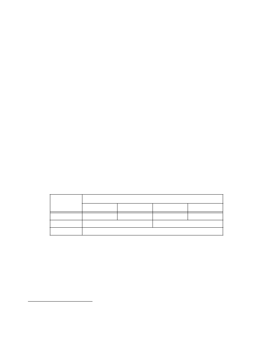
The NCO's spur level is reduced to below -92 dBc through the use of phase dithering. The spectrums in
Figure 5 show the NCO spurs for an example tuning frequency before and after dithering has been turned on. Notice
that the spur level decreases from -82 dB to -105 dB.
Figure 5. Example NCO Spurs
32 BITS
15 BITS
32 BITS
FREQUENCY
WORD
SINE/COSINE
OUT
18 MSBs
5 BITS
14 MSBs
DITHER
GENERATOR
PHASE
OFFSET
16 BITS
SINE/COSINE
LOOKUP
TABLE
(a) Before Dithering
(b) After Dithering
-82 dB
-105 dB
GRAYCHIP, INC.
- 6 -
APRIL 27, 1999
GC4014 QUAD RECEIVER CHIP
DATA SHEET REV 0.6
This document contains information which may be changed at any time without notice
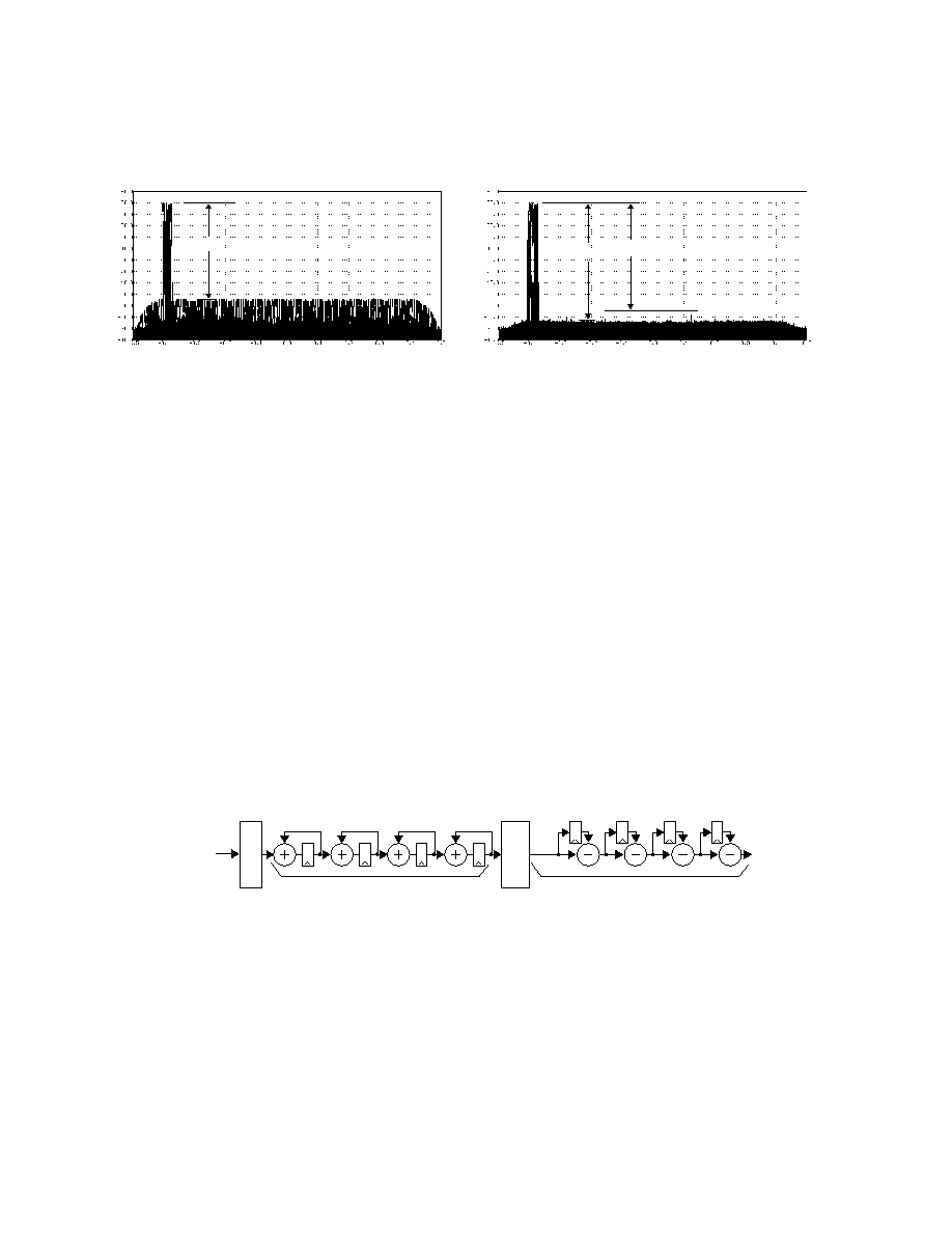
Figure 6 shows the maximum spur levels as the tuning frequency is scanned over a portion of the frequency
range with the peak hold function of the spectrum analyzer turned on. Notice that the peak spur level is -82 dB before
dithering and is between -92 and -102 after dithering has been turned on.
Figure 6. NCO Peak Spur Scan Plot
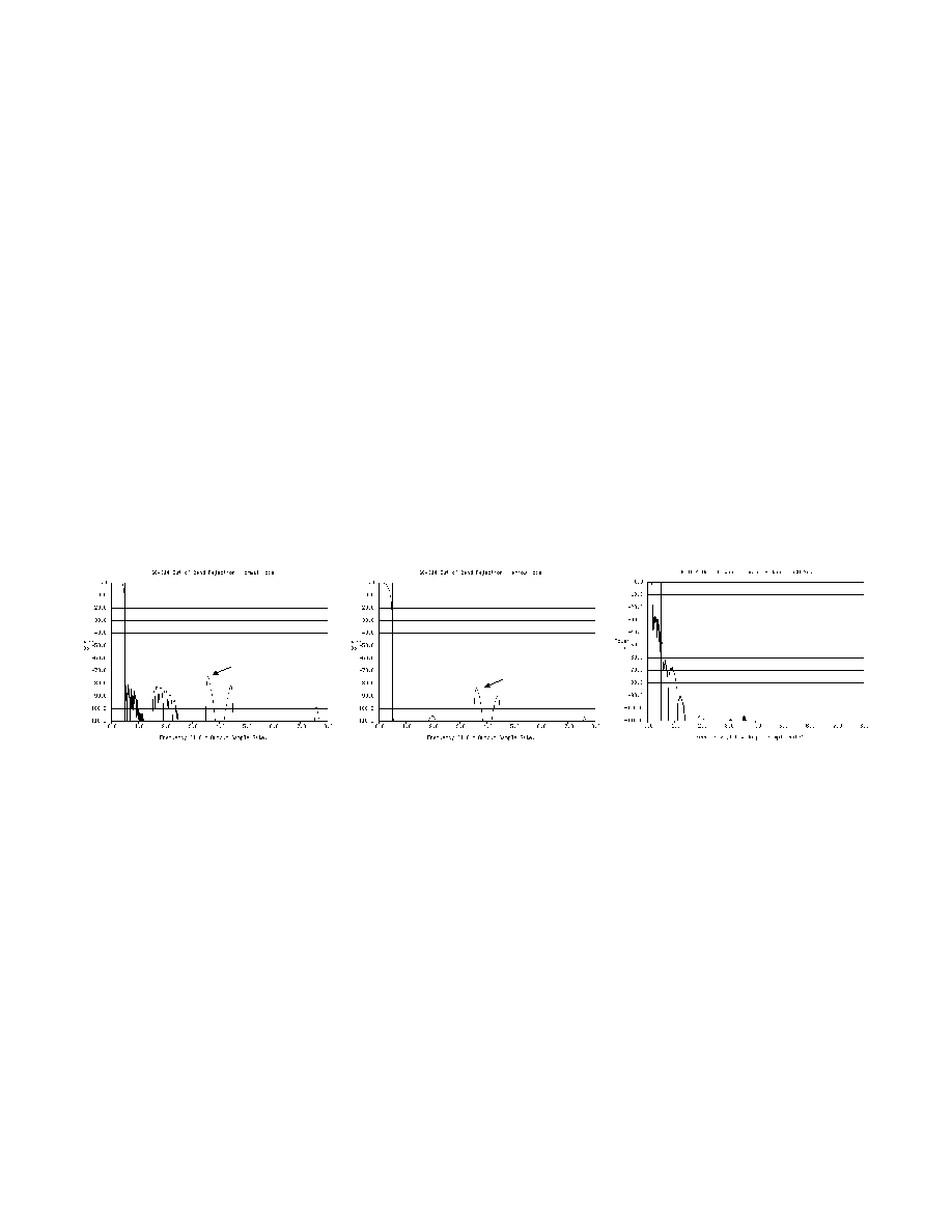
The worst case NCO spurs at -92 dB, such as the one shown in figure 6(b), are due to a few frequencies
that are related to the sampling frequency by small rational numbers (for example FREQ = 3/16 * Fck). In these
cases the rounding errors in the sine/cosine lookup table repeat in a regular fashion, thereby concentrating the error
power into a single frequency, rather than spreading it across the spectrum. These worst case spurs can be
eliminated by selecting an initial phase that minimizes the errors or by changing the tuning frequency by a small
amount (50 Hz). All spurs can be made to fall below -96 dB with the selection of a proper initial phase or tuning
frequency.
3.3.2
Four Stage CIC Filter
The mixer outputs are decimated by a factor of N in a four stage CIC filter, where N is any integer between
8 and 16,384. The programmable decimation allows the chip's usable output bandwidth to range from less than a
kilo-Hertz to 1.5 MHz when the input rate (which is equal to the chip's clock rate) is 62.5 MHz. A block diagram of
the CIC filter is shown in Figure 7.
Figure 7. Four Stage CIC Decimate by N Filter
The CIC filter has a gain equal to N
4
which must be compensated for in the "CIC_SCALE" circuit shown in
Figure 7. This circuit has a gain equal to 2
(SCALE+6*BIG_SCALE-56)
, where SCALE ranges from 0 to 5 and BIG_SCALE
ranges from 0 to 7. The gain of the CIC circuit is equal to:
. The user must select
values for SCALE and BIG_SCALE such that GAIN is less than one, i.e., SCALE and BIG_SCALE must be selected
such that:
. Overflows due to improper gain settings will go undetected if this
relationship is violated. For example, if N is equal to 8, then this restriction means that BIG_SCALE and SCALE
(a) Before Dithering
(b) After Dithering
-92 dB
-102 dB
-82 dB
UPPER
24 BITS
CIC_SCALE
DATA
IN
DATA
OUT
DECIMATE
BY FACTOR
OF N
CLOCKED AT FULL RATE
CLOCKED AT 1/N RATE
24 BITS
16 BITS
GAIN
N
4
2
SCALE 6
BIG_SCALE
56
≠
◊
+
(
)
=
SCALE
6
BIG_SCALE
◊
+
(
)
56
4log
2
N
≠
(
)
GRAYCHIP, INC.
- 7 -
APRIL 27, 1999
GC4014 QUAD RECEIVER CHIP
DATA SHEET REV 0.6
This document contains information which may be changed at any time without notice
should be less than or equal to 7 and 2 respectively. The BIG_SCALE and SCALE settings are common to all
channels.
3.3.3
Coarse Channel Gain
The gain of each channel can be boosted up to 42 dB by shifting the output of the CIC filter up by 0 to 7 bits
prior to rounding it to 16 bits. The coarse gain is:
, where COARSE ranges from 0 to 7. Overflows
in the coarse gain circuit are saturated to plus or minus full scale. The coarse gain is used to increase the gain of
an individual signal after the input bandwidth of the downconverter has been reduced by a factor of N in the CIC
filter. If the signal power across the input bandwidth is relatively flat, as is the case in most frequency division
multiplexed (FDM) systems, then one would want to boost the signal power out of the CIC filter by a factor of
. Each channel can be given its own coarse gain setting. Note that the final gain stage described in
Section 3.4 can boost the overall gain by up to 24 more dB.
3.3.4
The Compensating Decimate By Two Filter (CFIR)
The CIC/Coarse gain outputs are filtered by two stages of filtering. The first stage is a 21 tap decimate by
2 filter with two sets of fixed coefficients. The first set of coefficients is used in the normal mode to give a passband
which is flat (0.01 dB ripple) over 100% of the final output bandwidth and which has 85 dB of out of band rejection.
The filter also compensates for the droop associated with the CIC programmable decimation filter. The filter is
symmetric with the following taps:
29, -85, -308, -56, 1068, 1405, -2056, -6009, 1303, 21121, 32703
The narrow set of coefficients are intended for applications that need deeper stop bands or need
oversampled outputs. These requirement are common in cellular systems where out of band rejection requirements
can exceed 100 dB. The filter coefficients for the narrow mode are:
-98, -679, -2016, -3234, -2537, 850, 6053, 12060, 18230, 23239, 25212
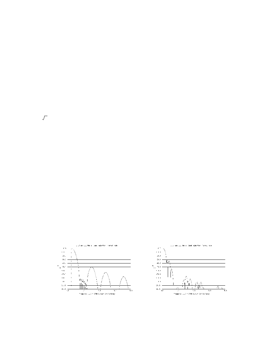
The combined frequency response of the CIC and CFIR filter for both modes is shown below:
Figure 8. Combined CFIR and CIC Frequency Response
GAIN
2
COARSE
=
GAIN
N
=
(a) Normal Mode
(b) Narrow Mode
GRAYCHIP, INC.
- 8 -
APRIL 27, 1999
GC4014 QUAD RECEIVER CHIP
DATA SHEET REV 0.6
This document contains information which may be changed at any time without notice
The dashed vertical line in the plots shows the output Nyquist rate for the chip when the PFIR is in the
decimate by 2 mode. The narrow mode filter introduces a gain of 1.97 (5.9 dB).
3.3.5
The Programmable Final Filter (PFIR)
The second stage decimate by two or four filter uses either internal ROM based coefficients, or externally
downloaded filter coefficients. The internal 80% bandwidth filter has 80 dB of out of band image rejection and 0.03
dB peak to peak passband ripple. The internal filter is a 63 tap symmetric filter. The 32 unique coefficients are:
-14, -20, 19, 73, 43, -70, -82, 84, 171, -49, -269, -34, 374, 192, -449,
-430, 460, 751, -357, -1144, 81, 1581, 443, -2026, -1337, 2437, 2886,
-2770, -6127, 2987, 20544, 29647
Figure 9(a) shows the overall response for the internal PFIR when the CFIR is in the normal mode. Figure
9(b) shows the overall response when the CFIR is in the narrow mode. Note that the peaks in the stop band at 3.5
times the output sample rate will, after decimation, fold into the transition band from 0.4 to 0.5 of the output sample
rate. This out of band power, if necessary, can be filtered out by either using a custom PFIR filter with a narrower
passband, or by post-filtering.
An overall response using custom coefficients suitable to meet the stringent GSM Cellular requirements is
shown in Figure 9(c). See Sections 7.5 and 7.6 for more details on GSM and DAMPS configurations.
Figure 9. Overall CIC-CFIR-PFIR Response
The externally downloaded coefficients can be used to tailor the spectral response to the user's needs. For
example, it can be programmed as a Nyquist (typically a root-raised-cosine) filter for matched filtering digital data.
The user downloaded filter coefficients are 16 bit 2's complement numbers. Unity gain will be achieved through the
filter if the sum of the 63 coefficients is equal to 65536. If the sum is not 65536, then the PFIR will introduce a gain
equal to (sum of coefficients)/65536.
The 63 coefficients are identified as coefficients h
0
through h
62
, where h
31
is the center tap. The coefficients
are assumed to be symmetric, so only the first 32 coefficients (h
0
through h
31
) are loaded into the chip. A
non-symmetric mode allows the user to download a 32 tap non-symmetric filter as taps h
0
through h
31
. ERRATA:
The non-symmetry mode does not work properly for parts marked with mask code 55532B, Contact GRAYCHIP for
details.
(a) Normal CFIR Mode
(b) Narrow CFIR Mode
Peaks fold into
transition band
Peaks fold into
transition band
(c) GSM Coefficients

GRAYCHIP, INC.
- 9 -
APRIL 27, 1999
GC4014 QUAD RECEIVER CHIP
DATA SHEET REV 0.6
This document contains information which may be changed at any time without notice
3.3.6
Real Mode
The PFIR will output either complex or real data. Complex data is output at a rate equal to F
CK
/(4N) or
F
CK
/(8N) in the decimate by 4 mode. If the output samples are real, then the filter translates the output spectrum up
by multiplying the filtered data by the complex sequence +1, -j, -1, +j,
...
, and then outputting the real part at a rate
equal to F
CK
/2N. The real output mode can be used to create double sided signals out of single sideband data. The
real outputs are packed into complex words for output. The first sample of a real pair is put into the I-half and the
second is put into the Q-half. Note that the decimate by 4 mode is invalid in the real mode.
3.4
FINAL GAIN ADJUSTMENT
The final gain of each channel is adjusted by multiplying each output sample by G/32, where G is a 10bit
2's complement gain word. Since G can range between -512 and +511, the gain adjustment will range from -16.0
to +15.98. Setting G to zero clears the channel. This provides a final gain adjustment range from -
to +24 dB in
approximately 0.28 dB steps. A different gain can be specified for each channel. Note that the overall gain of the
chip is also a function of the amount of decimation programmed into the chip (N), the scale circuit setting in the CIC
filter, the coarse gain setting, the narrow mode in the CFIR, and the sum of the PFIR coefficients. The overall gain
is shown below where the first term in braces is fixed for all four channels and must be less than or equal to unity.
The terms in square brackets can be different for each channel. NARROW is "1" in the narrow CFIR mode, "0"
otherwise. See Section 7.9 for a discussion on properly setting the chip's gain.
3.5
SUMMATION MODES
The chip can be programmed to output the four individual channels, the sum of pairs of channels, or the
sum of all four channels.These modes are used to process four real input signals, two complex input signals, or one
beamformed signal. When processing two complex input signals, the I inputs are put in channels A and C, and the
Q inputs are put in channels B and D. The summation mode then adds channels A and B together and channels C
and D together.
Summation is disabled in Sum Mode 0. In Sum Mode 1 the channel A output is replaced by the sum of
channels A and B, the channel B output is replaced by the sum of channels C and D, and the channel C and D
outputs are left alone. In Sum Mode 2 the channel A output becomes the sum of all four channels and channels B,
C and D are left alone. These modes are summarized in the following table:
Table 1: Output Summation Modes
SUM MODE
CHANNEL OUTPUT
OUT
A
OUT
B
OUT
C
OUT
D
0
CH
A
CH
B
CH
C
CH
D
1
CH
A
+ CH
B
CH
C
+ CH
D
CH
C
CH
D
2
CH
A
+ CH
B
+ CH
C
+ CH
D
CH
B
CH
C
CH
D
GAIN
N
4
2
SCALE
6
BIG_SCALE
◊
56
≠
+
(
)
{
}
2
COARSE
[
]
1.0
NARROW
0.97
◊
+
{
}
PFIR_SUM
65536
-------------------
{
}
G
32
------
[ ]
=
GRAYCHIP, INC.
- 10 -
APRIL 27, 1999
GC4014 QUAD RECEIVER CHIP
DATA SHEET REV 0.6
This document contains information which may be changed at any time without notice
3.6
OUTPUT MODES
The channel or summation outputs are accessible either through internal control registers, through bit serial
outputs, or through nibble serial (link mode) outputs. Note that the bit serial and link mode outputs start, after power
up, in a tri-state condition and must be turned on when the chip is configured.
3.6.1
Internal Control Registers
The internal control registers are loaded by the chip once every output sample period (OSP)
1
and held for
the rest of the period. The user is notified that new samples are ready and a new OSP has begun, either through an
interrupt signal provided by the chip's "READY" pin (RDY/ACK pin), or through a control register bit.
3.6.2
Serial Outputs
The chip provides a bit serial clock (SCK), a frame strobe (SFS) and four data bit lines (SOUT A,B,C and
D) to output the data. A MUX_MODE control specifies whether the four data outputs are transmitted on four separate
bit-serial pins, or multiplexed onto two, or just one pin in a TDM format. Separate output pins are not provided for
the I and Q halves of complex data. The I and Q outputs are always multiplexed onto the same bit-serial pin. The
16 bit I-component is output first, followed by the Q-component. The "packed mode" allows a complex pair to be
treated as a single 32 bit word. The "READY" signal is used to identify the first word of a complex pair or of the TDM
formatted output. The TDM modes are summarized in the following table (See Table 1 for a definition of OUT in the
summation modes):
The bit serial outputs use the format shown in Figure 10. Figure 10(a) shows the standard output mode (the
PACKED mode bit is low). The chip clocks the frame and data out of the chip on the rising edge of SCK (or falling
edge if the SCK_POL bit in the input control register is set). The chip sends the 16 bits (I data first) by setting SFS
high (or low if SFS_POL in the input control register is set) for one clock cycle, and then transmitting the data, MSB
first, on the next 16 clocks. The I/Q data is transmitted "back to back" as shown in Figure 10(a). If the PACKED
control bit is high, then the I and Q components are sent as a single 32 bit word with only one SFS strobe as shown
in Figure 10(b). If two or more channels are multiplexed out the same serial pins, then the subsequent I/Q channel
1. Output sample period (OSP) refers to the interval between output samples at the decimated output rate. For example,
if the input rate (and clock rate) is 10 MHz and the overall decimation factor is 100 (N=25) the OSP will be10
microseconds. An OSP starts when a new sample is ready and stops when the next one is ready.
Table 2: TDM Modes
MUX MODE
SERIAL OUTPUT
A
OUT
B
OUT
C
OUT
D
OUT
0
OUT
A
OUT
B
OUT
C
OUT
D
1
OUT
A
, OUT
B
OUT
C
, OUT
D
2
OUT
A
, OUT
B
, OUT
C
, OUT
D

GRAYCHIP, INC.
- 11 -
APRIL 27, 1999
GC4014 QUAD RECEIVER CHIP
DATA SHEET REV 0.6
This document contains information which may be changed at any time without notice
words will be transmitted immediately following the first I/Q pair as shown in Figure 10(c). Figure 10(c) also shows
how the RDY signal can be used to identify the I and Q channels in the TDM serial transmission.The bit-serial output
rate is programmable as a power-of-2 division of the input clock.
Figure 10. Serial Output Formats
The serial clock (SCK) will normally stop after the last bit transfer of each OSP. The user can force a
continuous clock by setting the CONTINUOUS control bit in the output control register. In the continuous mode the
data is repeated until the next OSP. This may be useful if the user wants to multiplex the outputs from multiple chips
onto the same serial bus. Note: The frame syncs are not intended to be used in the continuous mode. After the
proper number of frame syncs have been output as shown in Figure 10, the next frame sync will be missing in the
continuous mode. The frame syncs will then repeat every 16 (or 32 in the packed mode) bit clocks. Note also that
the number of bit clocks per output frame may not be a rational number, resulting in a truncated bit clock at the end
of the OSP.
3.6.3
Link Mode Output
The four serial output pins and the bit clock and frame sync pins can be configured as an ADSP-2106x
SHARC DSP chip link port. These pins are in a tri-state condition when the chip powers up. A control bit is set to
enable these pins and another control bit is set to enable the link port mode. In the link mode the READY output pin
becomes the ACK (acknowledge) input which is used to receive the link port "LACK" signal.
SCK
SFS
SOUT
I15
I14
I1
I0
Q15
Q14
(a) 16 BIT MODE, FRAME SYNC AT THE START OF EACH 16 BIT WORD
SCK
SFS
SOUT
I15
I14
I1
I0
Q15
Q14
(b) 32 BIT "PACKED" MODE, ONE FRAME SYNC AT THE START OF EACH 32 BIT TRANSFER
clock stops after transfers are complete and stays low unless "continuous" is set
clock stops after transfers are complete and stays low unless "continuous" is set
IA
QA
RDY is 4 clocks wide (CK not SCK clocks) or is 16 clocks wide if RDY_WIDTH is set
RDY
SFS
IA
QA
IB
QB
IA
QA
IB
QB
IC
QC
ID
QD
IA
(c) ONE, TWO OR FOUR CHANNEL MUX MODES (PACKED MODE IS ON)
SFS
SFS
SOUT
SOUT
SOUT
MUX_MODE=0
MUX_MODE=1
MUX_MODE=2
Output Sample Period (OSP)
Q1
Q0
I15
I14
The words repeat in the continuous mode
Q1
Q0
I15
I14
The words repeat in the continuous mode
IA
QA
IA
QA
IB
QB
QA
IB
QB
IC
QC

GRAYCHIP, INC.
- 12 -
APRIL 27, 1999
GC4014 QUAD RECEIVER CHIP
DATA SHEET REV 0.6
This document contains information which may be changed at any time without notice
The link port's timing is as follows: The GC4014 checks the state of the ACK pin at the start of an OSP. If
ACK is low, the chip does nothing. If ACK is high, then the chip will transmit one, two or four complex words out of
the link port. The words are either the channel outputs or the sums of channels depending upon the summation
mode settings. The number of outputs transmitted is determined by the MUX_MODE settings. If MUX_MODE is 0,
only OUT
A
will be transmitted. If MUX_MODE is 1, then OUT
A
and OUT
B
will be transmitted. If MUX_MODE is 2,
then all four will be transmitted. See Table 1 for a definition of OUT in the summation modes.
The data is transmitted in four bit nibbles on the rising edge of the bit clock. The transmission is completed
in 8, 16 or 32 clocks to transmit one, two or four complex pairs. If the ACK signal is low at the end of a word (after
clocks 8, 16, 24 and 32), then the clock will remain high and the transmission of the next word will be delayed until
ACK goes high again. If the ACK signal is low at the start of an OSP, then the transmission will be held off until the
next OSP. The clock remains low at the end of the transmission until the next OSP starts. The bit clock rate is
programmable as a division of the chip's clock.
3.7
CLOCKING
The chip can be clocked in one of two modes. In the standard mode, the clock rate is equal to the input data
rate which can be up to 62.5 MHz. An internal clock doubler doubles the clock rate so that the internal circuitry is
clocked at twice the data rate. To use the standard mode the CKMODE pin must be grounded and the internal
control register bit EN_DOUBLER must be set high (See Section 5.10).
The alternate clock mode (pin CKMODE is high) accepts a double rate clock on the CK2X pin and bypasses
the clock doubler circuit. The EN_DOUBLER control bit should be low. In the alternate mode the user must provide
both the standard clock and the double rate clock.
3.8
POWER DOWN MODES
The chip has a power down and keep alive circuit. This circuit contains a slow, nominally 1 KHz, oscillator
and a clock-loss detect cell. This circuit is used to detect the loss of clock and provide a slow keep-alive clock to the
chip. The circuit is also used to power down the chip by switching from the high speed input clock to the low speed
keep-alive clock. The low speed clock rate is slow enough to power down the chip while fast enough to refresh the
dynamic nodes within the chip. The user can select whether this circuit is in the automatic clock-loss detect mode,
is always on (power down mode), or is disabled (the slow clock never kicks in). The whole chip, or individual down
converter channels can be powered down. Using the power down mode for individual channels can save significant
power.
3.9
SYNCHRONIZATION
Each GC4014 chip can be synchronized through the use of a sync input signal, an internal one shot sync
generator, or a sync counter. Each circuit within the chip, such as the sine/cosine generators or the decimation
GRAYCHIP, INC.
- 13 -
APRIL 27, 1999
GC4014 QUAD RECEIVER CHIP
DATA SHEET REV 0.6
This document contains information which may be changed at any time without notice
control counter can be synchronized to one of these sources. These syncs can also be output from the chip so that
multiple chips can be synchronized to the syncs coming from a designated "master" GC4014 chip.
3.10
DATA LATENCY
The latency through the chip, including all pipeline delays and filtering group delays, is shown in the
following table (N is the CIC filter's decimation ratio, see Section 3.5, SI is the sync input to the chip, SO is the sync
output from the chip, and the RDY signal marks the beginning of each output frame, See Figure 10):
The last entry can be used to identify the group delay through the chip for time tagging events which pass
through the chip, where the time tag needs to be accurate to fractions of the output sample. Note that the overall
decimation in the complex output mode is one sample every 4N inputs. This means that the step edge will come out
21 samples plus (2N+15) clocks later. A good time tag algorithm would be to count the number of clock cycles
between the tagged input sample and the next RDY signal (the number D), and then tag the output sample that
comes 21 RDY signals later with a time tag which is adjusted by (D - 2N-15) clocks. To insure that the adjustment
is always positive, one would wait 22 RDY signals (22 outputs) and tag the sample with an adjustment of (D+2N-15)
clocks. Note that the output sample to be tagged is the sample that is output between the 22nd RDY signal and the
next RDY signal (see Figure 10).
3.11
DIAGNOSTICS
The chip has an internal ramp generator which can be used in place of the data inputs for diagnostics. An
internal checksum circuit generates a checksum of the output data to verify the chip's operation. Section 7.7 gives
suggested checksum configurations and their expected checksums.
Besides the internal diagnostics, the chip can support board level testing, an output test configuration which
can help initial debug as well as production test is described in Section 7.8.
Table 3: Latency
FROM INPUT
TO OUTPUT
LATENCY
UNITS
COMMENT
SI
SO
3
Clocks
sync in to sync out, Register settings:
OUTPUT_SYNC = 1,SO_INT_MODE =0
SI
RDY
3.5N+9
Clocks
Sync in to first valid RDY out
IN[0:13] at RDY
OUT (First)
5
Outputs
Data sample input coincident with RDY, to the first output
affected by it
IN[0:13] at RDY
OUT (Midpoint)
22
Outputs
-to the closest midpoint output affected by IN
IN[0:13] at RDY
OUT (Last)
37
Outputs
-to the last output affected by IN
IN[0:13] at RDY
OUT
(Step Response)
86N+15
Clocks
Step function delay, step edge is input coincident with
RDY, to the step edge output

GRAYCHIP, INC.
- 14 -
APRIL 27, 1999
GC4014 QUAD RECEIVER CHIP
DATA SHEET REV 0.6
This document contains information which may be changed at any time without notice
4.0
PACKAGING
The GC4014 chip comes in a 100 pin thin plastic quad flatpack package
P (0.5mm)
D
VCC PINS: 1, 26, 32, 39, 45, 51, 75
GND PINS: 25, 31, 38, 44, 50, 76, 86,100
100 PIN THIN QUAD FLAT PACK
NOTE: 0.01 to 0.1
µ
f DECOUPLING CAPACITORS SHOULD BE PLACED
AS CLOSE AS POSSIBLE TO EACH SIDE OF THE CHIP
92
91
89
86
84
83
81
79
77
76
90
88
87
85
82
80
78
95
94
93
17
16
14
11
9
8
6
4
2
1
VCC
SO
DIN11
DIN9
DIN8
DIN6
DIN3
DIN1
DIN0
15
13
12
10
7
5
3
SI
DIN13
DIN12
DIN10
DIN7
DIN5
DIN4
DIN2
20
19
CIN12
CIN11
18
CIN13
29
30
32
35
37
38
40
42
44
45
31
33
34
36
39
41
43
26
27
28
46
47
49
24
22
21
CIN10
CIN9
GND
BIN7
BIN9
BIN10
48
50
25
23
CIN8
CKMODE
GND
BIN8
64
65
67
70
72
73
75
99
97
96
A4
WR
VCC
SCK
AIN0
AIN2
AIN5
AIN7
AIN8
66
68
69
71
74
100
98
RD
CE
GND
SFS
AIN1
AIN3
AIN4
AIN6
61
62
AN10
AN11
63
AIN9
51
52
54
57
59
60
AIN12
AIN13
BIN1
BIN4
BIN6
VCC
53
55
56
58
BIN0
BIN2
BIN3
BIN5
A1
A
AIN13
59
AIN12
60
AIN11
61
AIN10
62
AIN9
63
AIN8
64
AIN7
65
AIN6
66
AIN5
67
AIN4
68
SI
3
CK
37
4
SO
C7
91
C6
90
C5
89
C4
88
C3
85
C2
84
C1
83
C0
82
CE
99
A4
96
A3
95
A2
94
GC4014
SFS
74
SCK
73
RDY/ACK
81
(MSB)
(MSB)
(MSB)
QUAD
GC4014-PQ: PLASTIC PACKAGE
GC4014-CQ: CERAMIC PACKAGE
VCC
BIN11
CK2X
GND
CK
CIN1
VCC
CIN4
CIN5
GND
BIN12
BIN13
VCC
CIN0
CIN2
CIN3
GND
CIN7
VCC
CIN6
GND
BOUT
RDY/ACK
C1
C2
GND
C5
C7
A0
AOUT
COUT
DOUT
C0
C3
VUP
C4
C6
A2
A3
A1
RECEIVER
A1
93
A0
92
WR
98
RD
97
AIN3
69
AIN2
70
AIN1
71
AIN0
72
CHIP
AOUT /L3
77
BOUT /L2
78
COUT /L1
79
DOUT /L0
80
CK2X
40
CKMODE
2
VUP PIN: 87
L
D1
DIMENSION
PLASTIC
D
CERAMIC
(width pin to pin)
16.0 mm (0.630")
D1 (width body)
14.0 mm (0.551")
P
(pin pitch)
0.5 mm (0.020")
B
(pin width)
0.22 mm (0.009")
L
(leg length)
0.60 mm (0.024")
A
(height)
1.5 mm (0.059")
A1 (pin thickness)
0.15 mm (0.006")
17.2 mm (0.677")
14.0 mm (0.551")
0.5 mm (0.020")
0.20 mm (0.008")
0.70 mm (0.028")
3.1 mm (0.122")
0.2 mm (0.008")
BIN13
41
BIN12
42
BIN11
43
BIN10
46
BIN9
47
BIN8
48
BIN7
49
BIN6
52
BIN5
53
BIN4
54
(MSB)
BIN3
55
BIN2
56
BIN1
57
BIN0
58
CIN13
19
CIN12
20
CIN11
21
CIN10
22
CIN9
23
CIN8
24
CIN7
27
CIN6
28
CIN5
29
CIN4
30
(MSB)
CIN3
33
CIN2
34
CIN1
35
CIN0
36
DIN13
5
DIN12
6
DIN11
7
DIN10
8
DIN9
9
DIN8
10
DIN7
11
DIN6
12
DIN5 /CIN-1
13
DIN4 /CIN-2
14
(MSB)
DIN3 /BIN-1
15
DIN2 /BIN-2
16
DIN1 /AIN-1
17
DIN0 /AIN-2
18
PINS POWERED BY V
UP
GC4014-PQ
QUAD RCVR
MMMMMM LLL
GRAYCHIP YYWW
MMMMM = Mask Code
LLL = Lot Code
YYWW = Date Code

GRAYCHIP, INC.
- 15 -
APRIL 27, 1999
GC4014 QUAD RECEIVER CHIP
DATA SHEET REV 0.6
This document contains information which may be changed at any time without notice
SIGNAL
DESCRIPTION
AIN, BIN, CIN, DIN
INPUT DATA,
Active high
The 14 bit 2's complement input data for the four channels. The data is clocked into the chip on the rising edge
of the clock (CK). The LSBs of DIN are used as the LSBs of AIN, BIN and CIN in the16 bit input mode (the pins
DIN0/AIN-2, DIN2/BIN-2 and DIN4/CIN-2 are the LSBs of the 16 bit AIN, BIN and CIN inputs).
AOUT, BOUT, COUT, DOUT
BIT SERIAL OUTPUT DATA,
Active high
The bit serial output data are transmitted on these pins. In the serial mode these are individual outputs, in the link
mode these form a four bit nibble (DOUT/L0 is the LSB of the Nibble, AOUT/L3 is the MSB). The output bits are
clocked out on the rising edge of SCK (falling edge if SCK_POL=1). These pins are tri-stated at power up and are
enabled by the OUTPUT_ENABLE control register bit.
SCK
BIT SERIAL DATA CLOCK
, Active high or low
The serial data bits are clocked out of the chip by this clock. The active edge of the clock is user programmable.
This pin is tri-stated at power up and is enabled by the OUTPUT_ENABLE control register bit.
SFS
BIT SERIAL FRAME STROBE
, Active high or low
The bit serial word strobe. This strobe delineates the 16 or 32 bit words within the bit serial output streams. This
strobe is a pulse at the beginning of each bit serial word. The polarity of this signal is user programmable. This
pin is tri-stated at power up and is enabled by the OUTPUT_ENABLE control register bit.
RDY/ACK
READY OR ACKNOWLEDGE FLAG
, programmable active high or low
The chip asserts this signal in the serial output mode to identify the beginning of an output sample period (OSP).
The width in input clock cycles and polarity of this signal are user programmable. This signal is typically used as
an interrupt to a DSP chip, but can also be used as a start pulse to dedicated circuitry. In the link mode this pin is
an input pin and is tied to the LACK handshake output from an ADSP-2106x SHARC DSP link port. This pin is
tri-stated at power up and is enabled in the serial mode by the OUTPUT_ENABLE control register bit.
CK
INPUT CLOCK.
Active high
The clock input to the chip. The AIN, BIN, CIN, DIN and SI input signals are clocked into the chip on the rising
edge of this clock.
CK2X
DOUBLE RATE INPUT CLOCK.
Active high
The double rate clock input to the chip. Used in the alternate clock mode to clock the chip. This clock must be
exactly twice the frequency of the CK clock. Should be grounded in the normal clock mode.
CKMODE
CLOCK MODE,
Active high
The clock mode control. The chip uses CK2X when this pin is tied high (alternate mode) to clock the internal
circuitry. When this signal is grounded (normal mode) the chip doubles the CK clock to use as the internal clock.
SI
SYNC IN.
Active low
The sync input to the chip. All timers, accumulators, and control counters are, or can be, synchronized to SI. This
sync is clocked into the chip on the rising edge of the input clock (CK).
SO
SYNC OUT.
Active low
This signal is either a delayed version of the input sync SI, the sync counter's terminal count (TC), or a one-shot
strobe. The SO signal is clocked out of the chip on the rising edge of the input clock (CK).
C[0:7]
CONTROL DATA I/O BUS.
Active high
This is the 8 bit control data I/O bus. Control register data is loaded into the chip or read from the chip through
these pins. The chip will only drive these pins when CE is low and RD is low and WR is high.
A[0:4]
CONTROL ADDRESS BUS.
Active high
These pins are used to address the control registers within the chip. Each of the control registers within the chip
are assigned a unique address. A control register can be written to or read from by setting A[0:4] to the register's
address.
RD
READ ENABLE.
Active low
This pin enables the chip to output the contents of the selected register on the C[0:7] pins when CE is also low.
WR
WRITE ENABLE.
Active low
This pin enables the chip to write the value on the C[0:7] pins into the selected register when CE is also low.
CE
CHIP ENABLE.
Active low
This control strobe enables the read or write operation. The contents of the register selected by A[0:4] will be
output on C[0:7] when RD is low and CE is low. If WR is low and CE is low, then the selected register will be
loaded with the contents of C[0:7].
Vup
MICROPROCESSOR INTERFACE POWER SUPPLY.
Power Supply
This pin provides power for the microprocessor interface to allow it to interface to 5 volt logic. Input pins (A[0:4],
RD,WR,CE,C[0:7], and RDY/ACK) must not be driven above Vup+0.3V. The output pins (C[0:7], RDY/ACK) will
drive a logic one to Vup under no load.

GRAYCHIP, INC.
- 16 -
APRIL 27, 1999
GC4014 QUAD RECEIVER CHIP
DATA SHEET REV 0.6
This document contains information which may be changed at any time without notice
5.0
CONTROL REGISTERS
The chip is configured and controlled through the use of eight bit control registers. These registers are
accessed for reading or writing using the control bus pins (CE, RD, WR, A[0:4], and C[0:7]) described in the
previous section. The register names and their addresses are:
The Mode and Control Registers are addresses 0 to 15
ADDRESS
NAME
ADDRESS
NAME
0
Sync Mode
8
Blank Control
1
Decimation Mode
9
Channel Flush Control
2
Decimation Byte 0
10
Counter Byte 0
3
Decimation Byte 1
11
Counter Byte 1
4
Scale Control
12
Test Mode
5
Channel Gain
13
Page Map
6
Output Format
14
Status
7
Output Mode
15
Checksum
Addresses 16 to 31 are used in sixteen pages as determined by the page select control bits in the page map
register. The page assignments are:
PAGE
NAME
PAGE
NAME
0
Channel Outputs
8
Coefficients 0 to 7
1
Keepalive Status
9
Coefficients 8 to 15
2
unused
10
Coefficients 16 to 23
3
unused
11
Coefficients 24 to 31
4
Channel Control A
12
unused
5
Channel Control B
13
unused
6
Channel Control C
14
unused
7
Channel Control D
15
unused
The following sections describe each of these registers. The type of each register bit is either R, W, or R/W
indicating whether the bit is read only, write only, or read/write. All bits are active high.

GRAYCHIP, INC.
- 17 -
APRIL 27, 1999
GC4014 QUAD RECEIVER CHIP
DATA SHEET REV 0.6
This document contains information which may be changed at any time without notice
5.1
SYNC MODE REGISTER
The Sync mode control register determines how the circuits within the chip are synchronized. Each circuit
which requires synchronization can be configured to be synchronized to the sync input (SI), or to the terminal count
of the sync counter (TC). The sync to each circuit can also be set to be always on or always off. Each circuit is given
a two bit sync mode control which is defined as:
NOTE: the internal syncs are active high. The SI input has been inverted to be the active high sync SI.
ADDRESS 0:
Sync Mode
, suggested default = 0x65
BIT
TYPE
NAME
DESCRIPTION
0,1 (LSBs)
R/W
DEC_SYNC
Synchronizes the decimation control counter. The decimation counter
controls the filter timing of each channel and the serial timing of the
output signals.
2,3
R/W
COUNTER_SYNC
Synchronizes the sync counter. This counter is used to generate the
periodic "TC" sync pulses. Mode 2 in Table 4 is always OS.
4,5
R/W
OUTPUT_SYNC
The selected sync is inverted and output on the SO pin.
6
R/W
USE_ONESHOT
The terminal count mode in table 4 is replaced by the one shot pulse
(OS) when this bit is set.
7
R/W
ONE_SHOT
The one shot sync pulse (OS) is generated when this bit is set. This
bit must be cleared before another one shot pulse can be generated.
If the user wishes to allow the chip to free run, asynchronous to other chips, then the sync settings can be
set to zero. If one wishes to synchronize several chips to a single sync source, then the sync mode selections should
be set to one. The suggested default is to output the one-shot (USE_ONESHOT = 1, OUTPUT_SYNC=2) and set
all other syncs to SI. The user should tie the SO output pin of one GC4014 chip to the SI input pin of all other GC4014
chips in a system in order to cleanly synchronize and initialize one or more GC4014 chips. If there is only a single
GC4014 chip, then all sync mode selections can be set to "2" to receive the one-shot directly. A one-shot should be
sent after initialization and each time the decimation ratio is changed.
Table 4: Sync Modes
MODE
SYNC DESCRIPTION
0
"0" (never asserted)
1
SI
2
TC (or OS, if USE_ONESHOT is set)
3
"1" (always active)

GRAYCHIP, INC.
- 18 -
APRIL 27, 1999
GC4014 QUAD RECEIVER CHIP
DATA SHEET REV 0.6
This document contains information which may be changed at any time without notice
5.2
DECIMATION MODE REGISTER
Registers 1 and 2 control the decimation modes for the chip. These settings are common to all channels
ADDRESS 1:
Decimation Mode
, suggested default = 0x80, power up resets to 0.
BIT
TYPE
NAME
DESCRIPTION
0 LSB
R/W
REAL
Enables the PFIR's real output mode. (See Section 3.3.6). The real outputs are formatted
into complex pairs in the real mode. The I-output words contain are the even-time real
outputs and the Q-outputs contain the odd-time real outputs.
1
R/W
FILTER_SELECT
The user downloaded filter coefficients are used instead of the built in filter coefficients for
the second stage FIR filter when this bit is set.
2
R/W
RDY_POL
This control bit inverts the polarity of the RDY output. Normally RDY pulses high when a new
sample is ready and an output sample period (OSP) is starting. RDY will pulse low when
RDY_POL is high.
3
R/W
RDY_WIDTH
Normally the RDY pin will pulse active for four clock cycles. This control bit forces RDY to be
active for 16 clocks.
4
R/W
LINK_MODE
Output the data in the nibble-serial link mode. The RDY/ACK pin becomes an input pin in this
mode. NOTE: To use the link mode this bit must be set before the OUTPUT_ENABLE control
bit in register 8 is set, otherwise the RDY/ACK pin will be driven as an output, possibly
damaging the pin.
5
R/W
SO_INT_MODE
The SO output pin is used as an overflow interrupt pin when this bit is set. If an overflow due
to gain settings occurs in any of the channels the SO pin will go low if this bit is set.
6
R/W
NO_SYMMETRY
The second stage decimate by two filter is normally a 63 tap symmetric filter. It becomes a
32 tap non-symmetric filter when this bit is set. ERRATA: The non-symmetry mode does not
work properly for parts marked with mask code 55532B, parts with other mask codes work.
Contact GRAYCHIP for details.
7 MSB
R/W
EN_DOUBLER
This bit must be set to enable the clock doubler circuit when the CKMODE pin is low. This bit
is ignored when CKMODE pin is tied high.
5.3
CIC DECIMATION REGISTERS
Registers 2, and 3 contain the 14 bit CIC decimation ratio control.
ADDRESS 2:
Decimation Byte 0
, suggested default = 0x07
BIT
TYPE
NAME
DESCRIPTION
0-7
R/W
DEC[0:7]
The LSBs of the decimation control
ADDRESS 3:
Decimation Byte 1
, suggested default = 0x00
BIT
TYPE
NAME
DESCRIPTION
0-5
R/W
DEC[8:13]
The 6 MSBs of the decimation control
6,7
R
zero
These bits are read only zeros.
Where DEC is equal to N-1. The chip decimates the input data by a factor of 2N for real output data and 4N
for complex output data (or 8N if DEC_BY_4 is set in Register 13), where N ranges from 8 to 16384. This provides
an decimation range from 32 to 65,536 for complex output signals and 16 to 32,768 for real output signals.

GRAYCHIP, INC.
- 19 -
APRIL 27, 1999
GC4014 QUAD RECEIVER CHIP
DATA SHEET REV 0.6
This document contains information which may be changed at any time without notice
5.4
SCALE CONTROL REGISTER
Register 4 controls the CIC filter gain for the chip. These settings are common to all channels
ADDRESS 4:
CIC Scale
, suggested default = 0x71
BIT
TYPE
NAME
DESCRIPTION
0-2
R/W
SCALE
SCALE ranges from 0 to 5.
3
R/W
unused
4-6
R/W
BIG_SCALE
BIG_SCALE ranges from 0 to 7.
7
R/W
unused
The CIC filter has a gain which is equal to N
4
. To remove this gain the CIC inputs are pre-scaled down by
(56-SCALE-6*BIG_SCALE) bits before filtering. The overall gain of each channel is equal to:
where COARSE and G are unique for each channel (See Section 5.17). PFIR_SUM is the sum of the 63 PFIR
coefficients if FILTER_SELECT in Register 1 is set, and NARROW is the CFIR narrow mode bit in Register 13. The
values of SCALE and BIG_SCALE must be such that the term in braces is less than unity, i.e.,
. Overflows due to improper gain settings will go undetected if this
relationship is violated. For example, this restriction means that BIG_SCALE and SCALE should be less than or
equal to 7 and 2 respectively for N equal to 8. The BIG_SCALE and SCALE settings are common to all channels.
See Section 7.9 for a discussion on how to optimally set the gain of the chip.
5.5
CHANNEL GAIN REGISTER
Register 5 contains the most significant 2 bits of each channel's gain setting G. The least significant bits are
stored in each channel's control page (See Section 5.17).
ADDRESS 5:
Channel Gain
, suggested default = 0x00
BIT
TYPE
NAME
DESCRIPTION
0,1
R/W
GA[8:9]
2 MSBs of Channel A's gain.
3,4
R/W
GB[8:9]
2 MSBs of Channel B's gain.
4,5
R/W
GC[8:9]
2 MSBs of Channel C's gain.
6,7
R/W
GD[8:9]
2 MSBs of Channel D's gain.
Since the gain is G/32, and these bits are only used if G is greater than 256 (except for negative values),
then setting this register to zero still allows the user to add up to 18 dB of gain by just using the 8 LSB's set in the
channel control pages. If more than 18 dB is desired, then these control register bits can be used. See Section 7.9
for a discussion on how to optimally set the gain of the chip.
GAIN
N
4
2
SCALE
6
BIG_SCALE
◊
56
≠
+
(
)
{
}
2
COARSE
[
]
1.0
NARROW
0.97
◊
+
{
}
PFIR_SUM
65536
-------------------
{
}
G
32
------
[ ]
=
SCALE
6
BIG_SCALE
◊
+
(
)
56
4log
2
N
≠
(
)

GRAYCHIP, INC.
- 20 -
APRIL 27, 1999
GC4014 QUAD RECEIVER CHIP
DATA SHEET REV 0.6
This document contains information which may be changed at any time without notice
5.6
OUTPUT FORMAT REGISTER
This register controls the output bit serial format.
ADDRESS 6:
Output Format Register
, suggested default = 0x01
BIT
TYPE
NAME
DESCRIPTION
0-3 LSB
R/W
RATE[0:3]
The bit serial rate is set at F
CK
2
-RATE
, where RATE can range from 0 to 10. If RATE=0,
the SCK pin will not toggle and the serial rate is equal to the clock rate.
4
R/W
PACKED
Puts the serial outputs into 32 bit transfer mode where each complex pair is packed
into 32 bit words. The complex pair is formatted as I word in the upper byte and the Q
word in the lower byte. Each word is formatted as MSB first.
5
R/W
CONTINUOUS
The serial clock normally stops when the last bit of each transmission is complete and
stays low until the next OSP.
6
R/W
SCK_POL
This bit inverts the polarity of the serial clock. Normally SOUT and SFS change on the
rising edge of SCK. They change on the trailing edge when this bit is set.
7 MSB
R/W
SFS_POL
The SFS signal is treated as active low when this bit is set. Otherwise the signal is
treated as active high.
5.7
OUTPUT MODE REGISTER
This register controls the output summation, multiplexing and rounding.
ADDRESS 7:
Output Mode Register
, suggested default = 0x00
BIT
TYPE
NAME
DESCRIPTION
0,1 LSB
R/W
SUM_MODE
The channel outputs are replaced by the sum of outputs as shown in Table 1 of
Section 3.5
2,3
R/W
MUX_MODE
The outputs are multiplexed as described in Section 3.6.2.
4
R/W
RND8
Round into the 8 MSBs of the 16 bit output words.
5
R/W
RND10
Round into the 10 MSBs of the 16 bit output words.
6
R/W
RND12
Round into the 12 MSBs of the 16 bit output words.
7 MSB
R/W
RND14
Round into the 14 MSBs of the 16 bit output words.
Only one round control bit can be set. If none are set the output is 16 bits. Bits below the rounding point are
set to zero.
5.8
BLANKING CONTROL REGISTER
This register controls the blanking mode.
ADDRESS 8:
Blank Control Register
, suggested default = 0x50, power up reset to 0.
BIT
TYPE
NAME
DESCRIPTION
0-3 LSB
R/W
BLANK_RATE
The number of zeroes to insert between each sample in the
blanking mode. Ranges from 0 to 15.
4,5
R/W
BLANK_SYNC
The sync selection from Table 4 for synchronizing the zero
stuffing.
6
R/W
OUTPUT_ENABLE
Turns on the serial output pins including SFS and SCK. RDY is
also turned on if LINK_MODE is off (See Section 5.2).
7 MSB
R/W
RAM_TEST
Used for factory tests. Should be kept low.
Blanking is turned on for each channel using the channel mode register in each channel's control page.

GRAYCHIP, INC.
- 21 -
APRIL 27, 1999
GC4014 QUAD RECEIVER CHIP
DATA SHEET REV 0.6
This document contains information which may be changed at any time without notice
5.9
CHANNEL FLUSH CONTROL REGISTER
This register controls flushing the four channels. Each channel is flushed when the selected sync occurs
The sync is selected according to Table 4 in Section 5.1.
ADDRESS 9:
Channel Flush Register
, suggested default = 0x55
BIT
TYPE
NAME
DESCRIPTION
0,1 LSB
R/W
FLUSH_A[0:1]
The flush sync for channel A.
2,3
R/W
FLUSH_B[0:1]
The flush sync for channel B.
4,5
R/W
FLUSH_C[0:1]
The flush sync for channel C.
6,7 MSB
R/W
FLUSH_D[0:1]
The flush sync for channel D.
Each channel should be flushed when the chip is being initialized or when the decimation control is
changed. The flush lasts for 8N clocks after the sync occurs. The channel flush syncs will normally be left in a "never"
mode. If a channel is unused, then the user should leave the channel in the "always" flush mode which will clear the
datapath, clear the channel's output, and lower its power consumption. During diagnostics the channels will need
to be flushed at the beginning of each sync cycle.
The user may wish to flush a channel when a new frequency is selected in order to purge the datapath of
the last signal.
5.10
COUNTER MODE REGISTERS
Registers 10, and 11 set the counter's cycle period.
ADDRESS 10:
Counter Byte 0
, suggested default = 0xff
BIT
TYPE
NAME
DESCRIPTION
0-7
R/W
CNT[0:7]
The LSBs of the counter cycle period
ADDRESS 11:
Counter Byte 1
, suggested default = 0xff
BIT
TYPE
NAME
DESCRIPTION
0-7
R/W
CNT[8:15]
The 8 MSBs of the counter cycle period
The chip's internal sync counter counts in cycles of 128(CNT+1) clocks. A terminal count signal (TC) is
output at the end of each cycle. The counter can be synchronized to an external sync as specified in the Sync mode
Register (See Section 5.1). If CNT is set so that 128(CNT+1) is a multiple of twice the decimation ratio (i.e., a
multiple of 16N), then the terminal count of this counter can be output on the SO pin and used to periodically
synchronize multiple GC4014 chips.

GRAYCHIP, INC.
- 22 -
APRIL 27, 1999
GC4014 QUAD RECEIVER CHIP
DATA SHEET REV 0.6
This document contains information which may be changed at any time without notice
5.11
TEST MODE REGISTER
Register 12 controls the test and diagnostic features of the chip.
ADDRESS 12:
Test Mode Register
, suggested default = 0x08, power up reset to 0.
BIT
TYPE
NAME
DESCRIPTION
0,1 LSB
R/W
DIAG_SOURCE
This two bit field selects the diagnostic input source used when the
DIAG bit in each channel's control register is set (See Section 5.17).
DIAG_SOURCE = 0 selects the 14 LSB's of the counter (see Section
5.10) as a diagnostic ramp. DIAG_SOURCE=1 is a zero input,
DIAG_SOURCE=2 is unused, DIAG_SOURCE= 3 gives a 0x4000
constant input.
2,3
R/W
DIAG_SYNC
The Checksum generator is strobed by this sync. See Table 4 for
the possible sync selections.
4
R/W
COUNT_TEST
Used during factory tests. Should be cleared during normal
operation.
5
R/W
PD_CLOCK_OFF
Turns off the clock in the power down mode.
6,7
R/W
POWER_DOWN
This two bit field controls the power down and keep alive circuit as
follows:
POWER_DOWN
MODE
0
Clock loss detect mode
1
Power down mode
2
Disabled
3
Test
The power_down mode defaults to 0 (clock loss detect mode) upon
power up.
5.12
PAGE MAP REGISTER
This register selects which page is been accessed by addresses 16 through 31. This register also contains
several miscellaneous control bits.
ADDRESS 13:
Page Map Register
BIT
TYPE
NAME
DESCRIPTION
0-3 LSBs
R/W
PAGE
The page selection. PAGE=0 selects the channel output data
page, PAGE=1 selects the status page, page=4,5,6 and 7 select
the channel control pages, pages 8,9,10 and 11 select the PFIR
coefficient pages.
4
R/W
NARROW
Selects the narrow mode CFIR coefficients.
5
R/W
DEC_BY_4
Enables the decimate by 4 mode of the PFIR.
6
R/W
16_BIT_INPUT
Enables the 16 bit input mode. DIN[6-13] are unused. DIN[0,1],
DIN[2,3], and DIN[4,5] become two additional LSB's for AIN,
BIN, and CIN respectively.
7 MSB
R/W
MSB_POL
Invert the input MSB polarity. This will convert an offset binary
formatted input to 2's complement format.

GRAYCHIP, INC.
- 23 -
APRIL 27, 1999
GC4014 QUAD RECEIVER CHIP
DATA SHEET REV 0.6
This document contains information which may be changed at any time without notice
5.13
STATUS CONTROL REGISTER
This register contains miscellaneous control and status information.
ADDRESS 14:
Status Control Register
, suggested default = 0x00
BIT
TYPE
NAME
DESCRIPTION
0 LSB
R/W
READY
The user sets this bit after reading the output registers. The chip
clears this bit when new values have been loaded and it is time
to read them.
1
R/W
MISSED
The chip sets this bit If the user has not set the READY bit before
the chip loads the output registers. This bit high indicates that an
error has occurred.
2
R/W
unused
3
R/W
GAIN_OVERFLOW
Indicates an overflow in the final gain circuit.
4
R/W
OVERFLOW_A
Indicates overflow in channel A's coarse gain.
5
R/W
OVERFLOW_B
Indicates overflow in channel B's coarse gain.
6
R/W
OVERFLOW_C
Indicates overflow in channel C's coarse gain.
7 MSB
R/W
OVERFLOW_D
Indicates overflow in channel D's coarse gain.
The READY bit is used to tell an external processor when new output samples are ready to be read. If
desired, the RDY pin can be used as an interrupt to the external processor (See Section 5.2) to tell the processor
when to read new samples. The user does not need to set the READY bit if RDY is used. If READY is not set,
however, the MISSED flag will not be valid.
The overflow bits are set when an overflow occurs and stays set until the user clears them. If the
SO_INT_MODE bit in control register 1 is set, then the SO pin will go low if OVERFLOW_A, OVERFLOW_B,
OVERFLOW_C, or OVERFLOW_D go active. GAIN_OVERFLOW will not cause SO to go low.
GAIN_OVERFLOW is set if the final gain circuit detects an overflow in any channel (or sum of channels if
SUM_MODE is active).
5.14
CHECKSUM REGISTER
The checksum register is a read only register which contains the checksum of the output data. The
checksum is stored in the checksum register and then starts over again each time the DIAG_SYNC (See
Section 5.11) occurs. This is a read only register.
ADDRESS 15:
Checksum Register
BIT
TYPE
NAME
DESCRIPTION
0-7
R
CHECKSUM[0:7]
The checksum.

GRAYCHIP, INC.
- 24 -
APRIL 27, 1999
GC4014 QUAD RECEIVER CHIP
DATA SHEET REV 0.6
This document contains information which may be changed at any time without notice
5.15
CHANNEL OUTPUT PAGE (PAGE = 0)
Addresses 16 through 31 are used to read output values. The outputs are 16 bit two's complement
numbers which are read as two 8 bit bytes, the lower address contains the lower byte. See Table 1 for the output
value definitions when SUM_MODE is used. The address assignments are:
ADDRESSES
NAME
ADDRESSES
NAME
16,17
A
OUT
, I-half
24,25
C
OUT
, I-half
18,19
A
OUT
, Q-half
26,27
C
OUT
,Q-half
20,21
B
OUT
, I-half
28,29
D
OUT
, I-half
22,23
B
OUT
,Q-half
30,31
D
OUT
,Q-half
These are all read only registers.
5.16
KEEPALIVE STATUS PAGE (PAGE = 1)
ADDRESS 16:
Clock Status
BIT
TYPE
NAME
DESCRIPTION
0
R
KACK
This bit monitors the keepalive clock.
1
R
KA_MODE
This bit monitors the keepalive mode.
2-7
-
unused
These bits are used for factory test purposes only.
ADDRESS 17:
Mask Revision
BIT
TYPE
NAME
DESCRIPTION
0-7
R
REVISION
Mask revision number.
This address can be used to determine the mask revision number for the GC4014. The mask revision
numbers are shown in Table 5 below (the mask codes are printed on the GC4014 package).
Table 5: Mask Revisions
Mask
Revision
Number
(Address 17)
Release Date
Mask Code
on Package
Description
0
October 1997
55532B
Original
0
January 1998
55532C
Corrected problems with non-symmetry mode, did not
change mask revision number in address 17.

GRAYCHIP, INC.
- 25 -
APRIL 27, 1999
GC4014 QUAD RECEIVER CHIP
DATA SHEET REV 0.6
This document contains information which may be changed at any time without notice
5.17
CHANNEL CONTROL PAGES (PAGES 4, 5, 6, 7)
Pages 4, 5, 6 and 7 contain the frequency, phase, gain and control settings for the four channels. To
configure channels A, B, C and D use pages 4, 5, 6 and 7 respectfully. All registers are read/write.
ADDRESSES 16, 17, 18, 19: Frequency
ADDRESS
NAME
DESCRIPTION
16
FREQ[0:7]
Byte 0 (LSBs) of FREQ
17
FREQ[8:15]
Byte 1 of FREQ
18
FREQ[16:23]
Byte 2 of FREQ
19
FREQ[24:31]
Byte 3 (MSBs) of FREQ
The 32 bit frequency control word is defined as:
FREQ = 2
32
F/F
CK
where F is the desired tuning frequency and F
CK
is the chip's clock rate (not the CK2X rate). Use positive frequency
values to downconvert signals. Use negative frequency values to invert the signal's spectrum. The 32 bit 2's
complement frequency words are entered as four bytes, the least significant byte in the lowest address, the most
significant in the highest address.
ADDRESSES 20, 21: Phase
ADDRESS
NAME
DESCRIPTION
20
PHASE[0:7]
Byte 0 (LSBs) of PHASE
21
PHASE[8:15]
Byte 1 (MSBs) of PHASE
The 16 bit phase offset is defined as:
PHASE = 2
16
P/2
where P is the desired phase in radian from 0 to 2
.
ADDRESS 22: Gain
, suggested default = 0x80
ADDRESS
NAME
DESCRIPTION
22
G[0:7]
Byte 0 (LSBs) of G
The upper two bits of G are stored in control register 5. Note that G is only part of the chip's gain and should
be used in conjunction with SCALE, BIG_SCALE and COARSE. See Sections 5.4 and 5.5 for details. See Section
7.9 for a discussion on how to optimally set the gain of the chip.

GRAYCHIP, INC.
- 26 -
APRIL 27, 1999
GC4014 QUAD RECEIVER CHIP
DATA SHEET REV 0.6
This document contains information which may be changed at any time without notice
ADDRESS 23:
Channel Control
, suggested default = 0x0, power up reset to 0.
BIT
TYPE
NAME
DESCRIPTION
0,1 LSB
R/W
INPUT
This two bit field selects which chip input should be used by the
channel. INPUT = 0,1,2 and 3 correspond to inputs A, B, C and
D.
2
R/W
DIAG
Use the diagnostic source as the channel input. See Address 12
(Section 5.11).
3
R/W
BLANK
Turn on blanking for this channel. See address 8, Section 5.8
4-6
R/W
COARSE
The COARSE gain setting used for this channel. See Sections
5.4 and 5.5 for details.
7 MSB
R/W
POWER_DOWN
Used to force the channel into the power down state.
ADDRESS 24:
Channel Sync Modes
, suggested default = 0x5f
BIT
TYPE
NAME
DESCRIPTION
0,1 LSB
R/W
FREQ_SYNC
The new frequency setting takes affect on this sync.
2,3
R/W
PHASE_SYNC
The new phase offset takes affect on this sync
4,5
R/W
NCO_SYNC
The NCO is initialized to the phase setting by this sync
6,7 MSB
R/W
DITHER_SYNC
The dither circuit is initialized by this sync to zero.
These syncs use the selections shown in Table 4.
The NCO_SYNC is usually set to be always off, unless the user wants to coherently control the phases of
multiple channels.
The FREQ_SYNC and PHASE_SYNC are typically set to be always on so that frequency and phase
settings will take effect immediately as they are written into their control registers.
The DITHER_SYNC is used to turn on or off the dithering of the NCO phase. To turn off dithering set the
DITHER_SYNC to be always on so that it remains initialized to zero. To turn dithering on set the sync to be always
off.
During diagnostics the NCO_SYNC and DITHER_SYNC should be set to "TC".

GRAYCHIP, INC.
- 27 -
APRIL 27, 1999
GC4014 QUAD RECEIVER CHIP
DATA SHEET REV 0.6
This document contains information which may be changed at any time without notice
5.18
COEFFICIENT STORAGE PAGES (PAGES 8, 9, 10 and 11)
Addresses 16 to 31 are used to download the 32 user programmable filter coefficients when PAGE is set to
8, 9, 10 and 11. Page 8 is for coefficients 0 through 7, page 9 is for coefficients 8 through 15, page 10 is for
coefficients 16 through 23, and page 11 is for coefficients 24 through 31, where coefficient 0 is the first coefficient
and coefficient 31 is the middle coefficient of the filter's impulse response. The 16 bit 2's complement coefficients
are stored in two bytes, least significant byte first, for example, the LSBs of coefficient 0 are stored in address 16
and the MSBs in address 17.
TO LOAD A COEFFICIENT THE USER MUST WRITE THE LSBYTE FIRST FOLLOWED BY THE
MSBYTE. Unknown values will be written into the LSBs if the MSB is written first. The coefficient registers are write
only.
GRAYCHIP, INC.
- 28 -
APRIL 27, 1999
GC4014 QUAD RECEIVER CHIP
DATA SHEET REV 0.6
This document contains information which may be changed at any time without notice
6.0
SPECIFICATIONS
6.1
ABSOLUTE MAXIMUM RATINGS
6.2
RECOMMENDED OPERATING CONDITIONS
6.3
THERMAL CHARACTERISTICS
Table 6: Absolute Maximum Ratings
PARAMETER
SYMBOL
MIN
MAX
UNITS
NOTES
DC Supply Voltage
V
CC
-0.3
4.1
V
Control I/O, CKMODE and RDY/ACK
Supply Voltage
V
UP
-0.3
6.0
V
Input voltage (undershoot and overshoot)
V
IN
-0.5
V
CC
+0.5
V
1
Storage Temperature
T
STG
-65
150
∞
C
Lead Soldering Temperature (10 seconds)
300
∞
C
Notes:
1. MAX is V
UP
+0.5 for the Control I/O and ACK pins.
Table 7: Recommended Operating Conditions
PARAMETER
SYMBOL
MIN
MAX
UNITS
NOTES
DC Supply Voltage
V
CC
3.1
3.5
V
1
Control I/O, CKMODE and RDY/ACK
Supply Voltage
V
UP
V
CC
5.5
V
Temperature Ambient, no air flow
T
A
-40
+85
∞
C
2
Junction Temperature
T
J
125
∞
C
2
1. DC and AC specifications are tested for this range. The GC4014 will operate at derated specifications
for lower supply voltages.
2. Thermal management may be required for full rate operation, See Table 8 below
Table 8: Thermal Data
THERMAL
CONDUCTIVITY
SYMBOL
GC4014-CQ
GC4014-PQ
UNITS
0.5 Watt
1 Watt
0.5 Watt
1 Watt
Theta Junction to Ambient
ja
54
37
40
32
∞
C
/W
Theta Junction to Case
jc
17
15
13
11
∞
C
/W
Note: Air flow will reduce
ja and is highly recommended.
GRAYCHIP, INC.
- 29 -
APRIL 27, 1999
GC4014 QUAD RECEIVER CHIP
DATA SHEET REV 0.6
This document contains information which may be changed at any time without notice
6.4
DC CHARACTERISTICS
All parameters are industrial temperature range of -40 to 85
o
C ambient unless noted.:
Table 9: DC Operating Conditions
PARAMETER
SYMBOL
Vcc = 3.1 to 3.5V
UNITS
NOTES
MIN
MAX
Voltage input low
V
IL
0.8
V
2
Voltage input high, AIN,BIN,CIN,DIN,SI,C
V
IH
2.1
V
2,3
Voltage input high CK, CK2X
V
IH
2.4
V
2
Input current (V
IN
= 0V)
I
IN
Typical +/- 20
uA
2
Voltage output low (I
OL
= 4mA)
V
OL
0.5
V
2
Voltage output high (I
OH
= -4mA)
V
OH
2.4
3.3
V
2,4
Data input capacitance (All inputs except CK)
C
IN
Typical 4
pF
1
Clock input capacitance (CK input)
C
CK
Typical 10
pF
1
Notes:
1. Controlled by design and process and not directly tested. Verified on initial parts evaluation.
2. Each part is tested at 85
∞
C for the given specification.
3. For V
UP
=5V, V
IH
=2.5V for the Control I/O, CKMODE and ACK pins.
4. For V
UP
=5V, V
OH
=2.8V (MIN) and V
OH
=5V (MAX) for the Control I/O and RDY pins.

GRAYCHIP, INC.
- 30 -
APRIL 27, 1999
GC4014 QUAD RECEIVER CHIP
DATA SHEET REV 0.6
This document contains information which may be changed at any time without notice
6.5
AC CHARACTERISTICS
Table 10: AC Characteristics (-40 TO +85
o
C Ambient, unless noted)
PARAMETER
SYMBOL
3.1V to 3.5V
UNITS
NOTES
MIN
MAX
Clock Frequency
F
CK
Note 5
64
MHz
2, 3
Clock low period (Below V
IL
)
t
CKL
6
ns
2
Clock high period (Above V
IH
)
t
CKH
6
ns
2
Clock rise and fall times (V
IL
to V
IH
)
t
RF
2
ns
1
Input setup before CK goes high
(AIN, BIN, CIN, DIN, or SI)
t
SU
2
ns
2
Input hold time after CK goes high
t
HD
2
ns
2
Data output delay from rising edge of CK.
(AOUT, BOUT, COUT, DOUT, SFS, SCK, RDY, or SO)
t
DLY
2
Note 1
15
Note 2
ns
4
Control Setup before both CE, WR or RD go low (See Figure 2.0)
t
CSU
3
ns
2, 8
Control hold after CE, WR or RD go high (See Figure 2.0)
t
CHD
3
ns
2, 8
Control strobe (CE or WR) pulse width (Write operation, See
Figure 2.0)
t
CSPW
20
ns
2, 8
Control output delay CE and RD low to C (Read Operation, See
Figure 2.0
t
CDLY
30
ns
2, 6, 8
Control tristate delay after CE and RD go high (See Figure 2.0)
t
CZ
10
ns
1
Quiescent supply current
(V
IN
=0 or V
CC
, F
CK
= 1KHz or POWER_DOWN=1)
I
CCQ
7
mA
1
Supply current
(F
CK
=64MHz, N=8)
I
CC
400
mA
2, 7
Notes:
1. Typical and not directly tested. Verified on initial part evaluation.
2. Each part is tested at 85 deg C for the given specification.
3. The chip may not operate properly at clock frequencies below MIN and above MAX.
4. Capacitive output load is 20pf. Delays are measured from the rising edge of the clock to the output level rising
above V
IH
or Falling below V
IL
.
5. The minimum clock rate must satisfy F
CK
/(4N) > 1KHz.
6. Capacitive output load is 80pf.
7. Current changes linearly with voltage and clock speed:
where A is the number of active channels (0 to 4) and N is the CIC decimation ratio.
8. See timing diagram in Figure 2 and description in Section 3.1.
Icc (MAX)
VCC
3.3
------------
F
CK
50
M
-----------
31
A 29
320
N
---------
+
+
mA
=

GRAYCHIP, INC.
- 31 -
APRIL 27, 1999
GC4014 QUAD RECEIVER CHIP
DATA SHEET REV 0.6
This document contains information which may be changed at any time without notice
7.0
APPLICATION NOTES
7.1
POWER AND GROUND CONNECTIONS
The GC4014 chip is a very high performance chip which requires solid power and ground connections to
avoid noise on the V
CC
and GND pins. If possible the GC4014 chip should be mounted on a circuit board with
dedicated power and ground planes and with at least two decoupling capacitors (0.01 and 0.1
µ
f) adjacent to each
GC4014 chip. If dedicated power and ground planes are not possible, then the user should place decoupling
capacitors adjacent to each V
CC
and GND pair.
IMPORTANT
The GC4014 chip may not operate properly if these power and ground guidelines are violated.
7.2
STATIC SENSITIVE DEVICE
The GC4014 chip is fabricated in a high performance CMOS process which is sensitive to the high voltage
transients caused by static electricity. These parts can be permanently damaged by static electricity and should only
be handled in static free environments.
7.3
SYNCHRONIZING MULTIPLE GC4014 CHIPS
A system containing two or more GC4014 chips will need to be synchronized if coherent operation is
desired. To synchronize multiple GC4014 chips connect all of the sync input pins together so they can be driven by
a common sync strobe. The common sync strobe can be from an external source, or can be the sync output from
one of the chips. If the sync output from one of the chips is used, then the user can choose to output a one shot sync
pulse from that chip, or the terminal count from the chip's sync counter. If the terminal count is used, then the sync
cycle must be a multiple of 8N and the FLUSH (Address 9), NCO_SYNC and DITHER_SYNC (Address 24 of each
channel page) syncs must be set to "never" (see Table 4) after initial synchronization.
7.4
THERMAL MANAGEMENT
The junction temperature must be kept below 125
∞
C for reliable operation. The chip's power dissipation
should be calculated using the equation for supply current in Section 6.5 and then the chip's junction temperature
can be calculated using the package's thermal conductivity shown in Section 6.3. At full rate operation (F
CK
=62.5)
the power is 1.3 Watts and the junction to ambient rise is 32 degrees per Watt for the plastic package. This
represents a rise of 42 degrees over ambient. This means that under these conditions the ambient temperature has
to be less than 83
∞
C. Air flow will decrease the thermal resistance by 10% to 40%, allowing ambient temperatures
between 87
∞
C and 100
∞
C. Increasing the decimation ratio (N) or decreasing the number of active channels (A) will
also allow a higher ambient temperature.
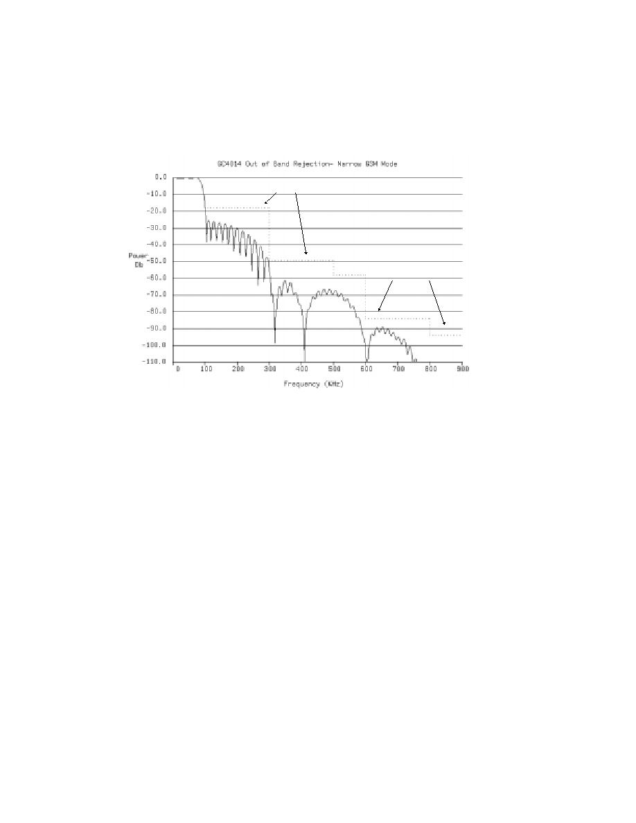
GRAYCHIP, INC.
- 32 -
APRIL 27, 1999
GC4014 QUAD RECEIVER CHIP
DATA SHEET REV 0.6
This document contains information which may be changed at any time without notice
7.5
GSM APPLICATION
The chip meets the stringent GSM out of band rejection requirements by using the narrow CFIR mode. The
overall response using the narrow CFIR mode and a programmable PFIR filter coefficient set targeted towards GSM
is shown in Figure 11, along with GSM's out of band rejection mask. In band ripple is 0.2 dB (peak to peak).
Figure 11. Overall Frequency Response for GSM
This response assumes the input sample rate is equal to 8*N*B, where N is the decimation in the CIC filter
(See Section 5.3) and B is the GSM bit rate (270.833 KHz). The data is output as two complex samples per bit
(541.667 KHz) when the PFIR is in the decimate by 2 mode (DEC_BY_4 = 0 in register 13), or is output as one
sample per bit (270.833 KHz) when the PFIR is in the decimate by 4 mode (DEC_BY_4=1).
The programmable PFIR coefficients for the GSM mode are:
1007, -1853, 79, 1807, 1633, 423, 265, 175, -527, -1331, -1454, -1087,
-721, -149, 1008, 1985, 2164, 2005, 1483, 61, -1756, -3134, -3953,
-4016, -2714, 134, 4003, 8361, 12934, 17009, 19565, 20353
GSM Adjacent Channel Requirements
GSM Blocker Requirements

GRAYCHIP, INC.
- 33 -
APRIL 27, 1999
GC4014 QUAD RECEIVER CHIP
DATA SHEET REV 0.6
This document contains information which may be changed at any time without notice
The suggested GSM control register settings for the chip with an input sample rate of 54.166 MHz (N=25)
is shown in Table 12 (other input rates can be used up to 62.5 MHz, 54.166 is used as an example):
The variables SCALE, BIG_SCALE (address 4) and G (address 16
HEX
of pages 4,5,6,and 7) are set as
follows. The values of SCALE and BIG_SCALE must be set to satisfy:
. N is
25, so (4log
2
N) is 37.14. This means
, which is satisfied by setting SCALE=1 and
BIG_SCALE=6. SCALE, however, needs to be decreased to 0 to prevent overflow in the CFIR, which has a gain of
1.97. The overall gain is set using "G" according to:
Where COARSE is 0 and PFIR_SUM is 125151. The optimal setting of GAIN is 2.0 in order to compensate for the
loss in the tuning process (See Section 7.9). A value of G=46 (2E
HEX
) will give a gain of 2.015.
The output serial format is set in address 6 to have a bit rate of one half the chip's clock rate and to be used
in the packed mode. The user will need to configure the output format as is necessary for the application.
Table 11: GSM Configuration
Control Registers
Channel pages 4,5,6,7
Coefficient Pages
Address
Data
Address
Data
Page 8
Page 9
Page 10
Page 11
00 (HEX)
65 (HEX)
1
10 (HEX)
FREQ[0:7]
EF
F1
74
66
01
80->82
2
11
FREQ[8:15]
03
FD
08
F5
02
19
12
FREQ[16:23]
C3
CD
D5
86
03
00
13
FREQ[24:31]
F8
FA
07
00
04
60
14
00 (HEX)
4F
52
CB
A3
05
00
15
00
00
FA
05
0F
06
11
16
2E
0F
C1
3D
A9
07
00
17
00
07
FB
00
20
08
50
18
5F
61
2F
24
86
09
55
19
06
FD
F9
32
0A
FF
1A
A7
6B
C2
71
0B
FF
1B
01
FF
F3
42
0C
08
1C
09
F0
8F
6D
0D
1P
3
1D
01
03
F0
4C
0E
00
1E
AF
C1
50
81
0F
read only
1F
00
07
F0
4F
1. Initialize to 65 while configuring the chip(s), then set to E5, then back to 65 to fire off the one-shot sync.This
assumes that SO is tied to SI
2. Initialize to 80, then set to 82 after external coefficients are loaded.
3. "P" is the page number. The upper nibble should stay at "1®.
SCALE
6
BIG_SCALE
◊
+
(
)
56
4log
2
N
≠
(
)
SCALE
6
BIG_SCALE
◊
+
(
)
37
GAIN
25
4
2
36
56
≠
(
)
{
}
2
COARSE
[
]
1.97
{
}
PFIR_SUM
65536
-------------------
{
}
G
32
------
0.0438G
=
=
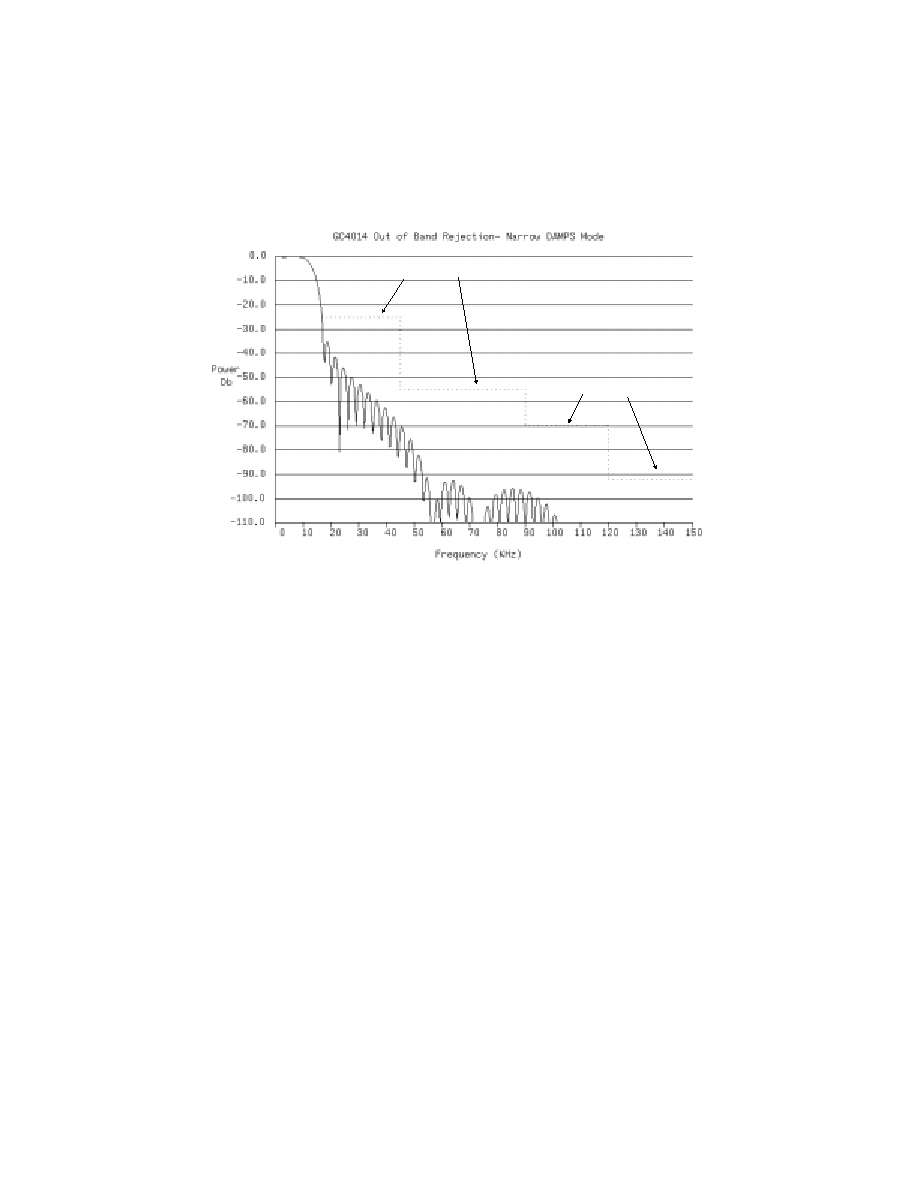
GRAYCHIP, INC.
- 34 -
APRIL 27, 1999
GC4014 QUAD RECEIVER CHIP
DATA SHEET REV 0.6
This document contains information which may be changed at any time without notice
7.6
DAMPS APPLICATION
The chip meets the DAMPS out of band rejection requirements by using the narrow CFIR mode. The overall
response using the narrow CFIR mode and a programmable PFIR filter coefficient set targeted towards DAMPS is
shown in Figure 12, along with the out of band rejection mask for DAMPS. The in-band response matches the
desired root-raised-cosine receive filter shape to within 0.1 dB.
Figure 12. Overall Frequency Response for DAMPS
This response assumes the input sample rate is equal to 16*N*B, where N is the decimation in the CIC filter
(See Section 5.3) and B is the DAMPS symbol (baud) rate (24.3 KHz). The data is output as four complex samples
per symbol (97.2 KHz) when the PFIR is in the decimate by 2 mode (DEC_BY_4 = 0 in register 13), or is output as
two samples per symbol (24.3 KHz) when the PFIR is in the decimate by 4 mode (DEC_BY_4=1).
The programmable PFIR coefficients for the DAMPS mode are:
264, 398, 413, 286, 34, -286, -584, -761, -729, -442, 85, 766, 1451,
1954, 2086, 1708, 768, -660, -2371, -4041, -5269, -5640, -4801, -2532,
1194, 6185, 12037, 18172, 23923, 28618, 31691, 32759
DAMPS Adjacent Channel Requirements
DAMPS Blocker Requirements

GRAYCHIP, INC.
- 35 -
APRIL 27, 1999
GC4014 QUAD RECEIVER CHIP
DATA SHEET REV 0.6
This document contains information which may be changed at any time without notice
The suggested DAMPS control register settings for the chip with an input sample rate of 49.7664 MHz
(N=128) is shown in the following table (other input rates can be used up to 62.5 MHz, 49.7664 is used as an
example):
The variables SCALE, BIG_SCALE (address 4) and G (address 16
HEX
of pages 4,5,6,and 7) are set as
follows. The values of SCALE and BIG_SCALE must be set to satisfy:
. N is
128, so (4log
2
N) is 28. This means
, which is satisfied by setting SCALE=4 and
BIG_SCALE=4. SCALE, however, needs to be decreased to 3 to prevent overflow in the CFIR, which has a gain of
1.97. The overall gain is set using "G" according to:
Where COARSE is 0 (see Section 7.9) and PFIR_SUM is 240593. The optimal setting of GAIN is 2.0 in order to
compensate for the loss in the tuning process (See Section 7.9). A value of G=18 (12
HEX
) will give a gain of 2.034.
The output serial format is set in address 6 to have a bit rate of one half the chip's clock rate and to be used
in the packed mode. The user will need to configure the output format as is necessary for the application.
Table 12: DAMPS Configuration
Control Registers
Channel pages 4,5,6,7
Coefficient Pages
Address
Data
Address
Data
Page 8
Page 9
Page 10
Page 11
00 (HEX)
65 (HEX)
1
10 (HEX)
FREQ[0:7]
08
27
00
AA
01
80->82
2
11
FREQ[8:15]
01
FD
03
04
02
7F
12
FREQ[16:23]
8E
46
6C
29
03
00
13
FREQ[24:31]
01
FE
FD
18
04
43
14
00 (HEX)
9D
55
BD
05
05
00
15
00
01
00
F6
2F
06
11
16
12
1E
FE
37
FC
07
00
17
00
01
02
F0
46
08
50
18
5F
22
AB
6B
73
09
55
19
00
05
EB
5D
0A
FF
1A
E2
A2
F8
CA
0B
FF
1B
FE
07
E9
6F
0C
08
1C
B8
26
3F
CB
0D
1P
3
1D
FD
08
ED
7B
0E
00
1E
07
AC
1C
F7
0F
read only
1F
FD
06
F6
7F
1. Initialize to 65 while configuring the chip(s), then set to E5, then back to 65 to fire off the one-shot sync.This
assumes that SO is tied to SI
2. Initialize to 80, then set to 82 after external coefficients are loaded.
3. "P" is the page number. The upper nibble should stay at "1®.
SCALE
6
BIG_SCALE
◊
+
(
)
56
4log
2
N
≠
(
)
SCALE
6
BIG_SCALE
◊
+
(
)
28
GAIN
128
4
2
27
56
≠
(
)
{
}
2
COARSE
[
]
1.97
(
)
PFIR_SUM
65536
-------------------
(
)
G
32
-----
0.113G
=
=
GRAYCHIP, INC.
- 36 -
APRIL 27, 1999
GC4014 QUAD RECEIVER CHIP
DATA SHEET REV 0.6
This document contains information which may be changed at any time without notice
7.7
DIAGNOSTICS
Four diagnostic tests are described here. These tests use the diagnostic ramp as the input data source and
the counter for synchronization. The tests are run by loading the configurations, waiting for the checksum to
stabilize, and then reading the checksum from address 15 and comparing it to the expected checksum shown in
each configuration table for address 15.
Table 13: Diagnostic Test 1 Configuration
Control Registers
Channel pages 4,5,6,7
Coefficient Pages
Address
Data
Address
Page 4
Page 5
Page 6
Page 7
Page 8
Page 9
Page 10
Page 11
00 (HEX)
2A (HEX)
10 (HEX)
12 (HEX)
45 (HEX)
AA (HEX)
55 (HEX)
Unused
01
80
11
23
23
55
AA
02
07
12
34
34
AA
55
03
00
13
01
02
00
03
04
72
14
55
55
55
55
05
00
15
55
55
55
55
06
00
16
FF
AA
55
80
07
00
17
04
04
04
04
08
51
18
AA
AA
AA
AA
09
AA
19
0A
FF
1A
0B
0F
1B
0C
88
1C
0D
0P
2
1D
0E
00
1E
0F
85
1
1F
1. This is the read-only expected checksum
2. P = desired page number
Table 14: Diagnostic Test 2 Configuration
Control Registers
Channel pages 4,5,6,7
Coefficient Pages
Address
Data
Address
Page 4
Page 5
Page 6
Page 7
Page 8
Page 9
Page 10
Page 11
00 (HEX)
2A (HEX)
10 (HEX)
55 (HEX)
12 (HEX)
45 (HEX)
AA (HEX)
Unused
01
80
11
AA
23
23
55
02
0F
12
55
34
34
AA
03
00
13
03
00
01
02
04
64
14
AA
AA
AA
AA
05
00
15
AA
AA
AA
AA
06
01
16
AA
55
7F
FF
07
00
17
04
04
04
04
08
51
18
AA
AA
AA
AA
09
AA
19
0A
FF
1A
0B
0F
1B
0C
88
1C
0D
0P
1D
0E
00
1E
0F
80
1
1F
1. This is the read-only expected checksum

GRAYCHIP, INC.
- 37 -
APRIL 27, 1999
GC4014 QUAD RECEIVER CHIP
DATA SHEET REV 0.6
This document contains information which may be changed at any time without notice
Table 15: Diagnostic Test 3 Configuration
Control Registers
Channel pages 4,5,6,7
Coefficient Pages
Address
Data
Address
Page 4
Page 5
Page 6
Page 7
Page 8
Page 9
Page 10
Page 11
00 (HEX)
2A (HEX)
10 (HEX)
12 (HEX)
45 (HEX)
AA (HEX)
55 (HEX)
AA
AA
AA
AA
01
80->82
2
11
23
23
55
AA
55
55
55
55
02
07
12
34
34
AA
55
AA
AA
AA
AA
03
00
13
00
01
02
03
55
55
55
55
04
72
14
55
55
55
55
AA
AA
AA
AA
05
00
15
55
55
55
55
55
55
55
55
06
00
16
FF
AA
55
80
AA
AA
AA
AA
07
00
17
04
04
04
04
55
55
55
55
08
51
18
AA
AA
AA
AA
AA
AA
AA
AA
09
AA
19
55
55
55
55
0A
FF
1A
AA
AA
AA
AA
0B
0F
1B
55
55
55
55
0C
88
1C
AA
AA
AA
AA
0D
0P
1D
55
55
55
55
0E
00
1E
AA
AA
AA
AA
0F
BA
1
1F
55
55
55
55
1. This is the read-only expected checksum
2. Initialize to 80, then set to 82 after coefficients have been loaded
Table 16: Diagnostic Test 4 Configuration
Control Registers
Channel pages 4,5,6,7
Coefficient Pages
Address
Data
Address
Page 4
Page 5
Page 6
Page 7
Page 8
Page 9
Page 10
Page 11
00 (HEX)
2A (HEX)
10 (HEX)
55 (HEX)
12 (HEX)
45 (HEX)
AA (HEX)
55
55
55
55
01
80->82
2
11
AA
23
23
55
AA
AA
AA
AA
02
FF
12
55
34
34
AA
55
55
55
55
03
00
13
03
00
01
02
AA
AA
AA
AA
04
40
14
AA
AA
AA
AA
55
55
55
55
05
00
15
AA
AA
AA
AA
AA
AA
AA
AA
06
00
16
AA
55
7F
FF
55
55
55
55
07
00
17
04
04
04
04
AA
AA
AA
AA
08
51
18
AA
AA
AA
AA
55
55
55
55
09
AA
19
AA
AA
AA
AA
0A
FF
1A
55
55
55
55
0B
0F
1B
AA
AA
AA
AA
0C
88
1C
55
55
55
55
0D
0P
1D
AA
AA
AA
AA
0E
00
1E
55
55
55
55
0F
D2
1
1F
AA
AA
AA
AA
1. This is the read-only expected checksum
2. Initialize to 80, then set to 82 after coefficients have been loaded

GRAYCHIP, INC.
- 38 -
APRIL 27, 1999
GC4014 QUAD RECEIVER CHIP
DATA SHEET REV 0.6
This document contains information which may be changed at any time without notice
7.8
OUTPUT TEST CONFIGURATION
The following configuration allows the user to debug the output interface to insure that the GC4014 data is
being received properly by the following circuitry. The configuration in the following table will generate a fixed output
sequence of four values (two complex pairs) which will repeat indefinitely:
The programmable PFIR coefficients are not used and do not need to be loaded. The user should change
address 6 (Output Format Register) to reflect the desired serial or link output mode. The expected results for various
decimation ratios are shown below:
The output sequence is the same for all power-of-two decimations. Other decimation ratios, with the SCALE
and BIG_SCALE values being the maximum which satisfy:
, will result in
sequences with the same I values, but with slightly different Q values.
Table 17: Output Test Configuration
Control Registers
Channel pages 4,5,6,7
Address
Data
Address
Data
00 (HEX)
6A (HEX)
1
10 (HEX)
00 (HEX)
01
81
11
00
02
0F
2
12
00
03
00
2
13
00
04
63
2
14
00
05
00
15
00
06
11
3
16
80
07
10
17
74
08
50
18
FF
09
AA
19
0A
FF
1A
0B
FF
1B
0C
0F
1C
0D
0P
4
1D
0E
00
1E
0F
read only
1F
1. Initialize to 6A while configuring the chip(s), then set to EA, then back to 6A to fire off the one-shot sync.
2. Gives an overall decimate by 64, See Table 18 for other values.
3. Value is application dependent.
4. "P" is the page number. The upper nibble should stay at "0®.
Table 18: Test Output Sequence
Decimation Controls
Output Sequence
Overall
Decimation
Addresses
2, 3
Address 4
I
0
Q
0
I
1
Q
1
32
07, 00
71
8000
FD00
7F00
0300
64
0F, 00
63
128
1F, 00
55
256
3F, 00
51
512
7F, 00
43
1024
FF, 00
35
2048
FF, 01
31
100
18, 00
60
8000
FE00
7F00
0200
SCALE
6
BIG_SCALE
◊
+
(
)
56
4log
2
N
≠
(
)

GRAYCHIP, INC.
- 39 -
APRIL 27, 1999
GC4014 QUAD RECEIVER CHIP
DATA SHEET REV 0.6
This document contains information which may be changed at any time without notice
7.9
OPTIMAL GAIN SETTINGS
The overall gain of the chip is the product of the CIC gain, the coarse gain, the CFIR gain, the PFIR gain
and the final gain. Each of these components are:
The signal flows through these sections in the order given. The gain settings which optimize the dynamic
range of the chip, are the ones that maximize the signal amplitude without clipping at the output of each of these
processing stages. A conservative approach to gain would be to set each gain component so that the product of the
gains at each processing point in the flow is less than or equal to unity.
The conservative approach, described above, is usually less than optimal. The optimal gain takes the
following considerations into account.
7.9.1
Tuning Loss
The input to the chip can be described as a signal S(t) modulated to a center frequency of "w". The input is,
therefore, S(t)cos(wt) = S(t)(e
jwt
+e
-jwt
)/2. If the downconverter tunes to the frequency "w", then the tuner output will
be S(t)(1.0+e
-2wt
)/2. The filters will then reject the component at "-2w", leaving just the signal S(t)/2. This loss of
one-half amplitude can be compensated for by setting the overall gain equal to 2, not unity. The tuning gain loss
occurs after the CIC filters, so the optimum gain approach is to use gain settings that keep the gain product after
the coarse, CFIR, PFIR and final gain stages equal to 2.
7.9.2
Uniform Power Inputs
The gain can be further optimized if the user has control over the power levels of the signals in the input
bands. If all of the signals in the input are close to equal power, then the gain of the downconverted signal can be
boosted to maximize its dynamic range. For example, if there are "M" signals of equal power in the input band, then
the amplitude of each signal is
. This means that the gain can be boosted by a factor of
within the
downconverter. The coarse gain can be used to add the additional gain.
Examples of applications which can use this feature are FM-FDM systems, cellular systems which use
power control, and wireless local loop systems that fix the power level of each remote transmitter.
CIC gain
N
4
2
SCALE
6
BIG_SCALE
◊
56
≠
+
(
)
=
Coarse gain
2
COARSE
=
CFIR gain
1.0
NARROW
0.97
◊
+
(
)
=
PFIR gain
PFIR_SUM
65536
----------------------------
=
Final gain
G
32
------
=
1
M
---------
M

GRAYCHIP, INC.
- 40 -
APRIL 27, 1999
GC4014 QUAD RECEIVER CHIP
DATA SHEET REV 0.6
This document contains information which may be changed at any time without notice
Page left intentionally blank

IMPORTANT NOTICE
Texas Instruments Incorporated and its subsidiaries (TI) reserve the right to make corrections, modifications,
enhancements, improvements, and other changes to its products and services at any time and to discontinue
any product or service without notice. Customers should obtain the latest relevant information before placing
orders and should verify that such information is current and complete. All products are sold subject to TI's terms
and conditions of sale supplied at the time of order acknowledgment.
TI warrants performance of its hardware products to the specifications applicable at the time of sale in
accordance with TI's standard warranty. Testing and other quality control techniques are used to the extent TI
deems necessary to support this warranty. Except where mandated by government requirements, testing of all
parameters of each product is not necessarily performed.
TI assumes no liability for applications assistance or customer product design. Customers are responsible for
their products and applications using TI components. To minimize the risks associated with customer products
and applications, customers should provide adequate design and operating safeguards.
TI does not warrant or represent that any license, either express or implied, is granted under any TI patent right,
copyright, mask work right, or other TI intellectual property right relating to any combination, machine, or process
in which TI products or services are used. Information published by TI regarding third≠party products or services
does not constitute a license from TI to use such products or services or a warranty or endorsement thereof.
Use of such information may require a license from a third party under the patents or other intellectual property
of the third party, or a license from TI under the patents or other intellectual property of TI.
Reproduction of information in TI data books or data sheets is permissible only if reproduction is without
alteration and is accompanied by all associated warranties, conditions, limitations, and notices. Reproduction
of this information with alteration is an unfair and deceptive business practice. TI is not responsible or liable for
such altered documentation.
Resale of TI products or services with statements different from or beyond the parameters stated by TI for that
product or service voids all express and any implied warranties for the associated TI product or service and
is an unfair and deceptive business practice. TI is not responsible or liable for any such statements.
Mailing Address:
Texas Instruments
Post Office Box 655303
Dallas, Texas 75265
Copyright
2001, Texas Instruments Incorporated