 | –≠–ª–µ–∫—Ç—Ä–æ–Ω–Ω—ã–π –∫–æ–º–ø–æ–Ω–µ–Ω—Ç: LT1009 | –°–∫–∞—á–∞—Ç—å:  PDF PDF  ZIP ZIP |
LT1009
2.5-V INTEGRATED REFERENCE CIRCUITS
SLVS013G ≠ MAY 1987 ≠ REVISED NOVEMBER 1999
1
POST OFFICE BOX 655303
∑
DALLAS, TEXAS 75265
D
Excellent Temperature Stability
D
Initial Tolerance . . . 0.2% Max
D
Dynamic Impedance . . . 0.6
Max
D
Wide Operating Current Range
D
Directly Interchangeable With LM136
D
Needs No Adjustment for Minimum
Temperature Coefficient
D
Surface-Mount Three-Lead Package
description
The LT1009 reference circuit is a
precision-trimmed 2.5-V shunt regulator featuring
low dynamic impedance and a wide operating
current range. The maximum initial tolerance is
±
5 mV in the LP package and
±
10 mV in the
D package. The reference tolerance is achieved
by on-chip trimming, which minimizes the initial
voltage tolerance and the temperature
coefficient
vz
.
Although the LT1009 needs no adjustments, a
third terminal (ADJ ) allows the reference voltage
to be adjusted
±
5% to eliminate system errors. In
many applications, the LT1009 can be used as a
terminal-for-terminal replacement for the
LM136-2.5, which eliminates the external trim
network.
The LT1009 uses include 5-V system references, 8-bit ADC and DAC references, and power-supply monitors.
The device also can be used in applications such as digital voltmeters and current-loop measurement and
control systems.
The LT1009C is characterized for operation from 0
∞
C to 70
∞
C. The LT1009I is characterized for operation from
≠ 40
∞
C to 85
∞
C.
AVAILABLE OPTIONS
PACKAGED DEVICES
CHIP
TA
SMALL
OUTLINE
(D)
PLASTIC
CYLINDRICAL
(LP)
CHIP
FORM
(Y)
0
∞
C to 70
∞
C
LT1009CD
LT1009CLP
LT1009Y
≠ 40
∞
C to 85
∞
C
LT1009ID
LT1009ILP
LT1009Y
The D and LP packages are available taped and reeled. Add the suffix R to device
type (e.g., LT1009CDR). Chip forms are tested at 25
∞
C.
Copyright
©
1999, Texas Instruments Incorporated
PRODUCTION DATA information is current as of publication date.
Products conform to specifications per the terms of Texas Instruments
standard warranty. Production processing does not necessarily include
testing of all parameters.
Please be aware that an important notice concerning availability, standard warranty, and use in critical applications of
Texas Instruments semiconductor products and disclaimers thereto appears at the end of this data sheet.
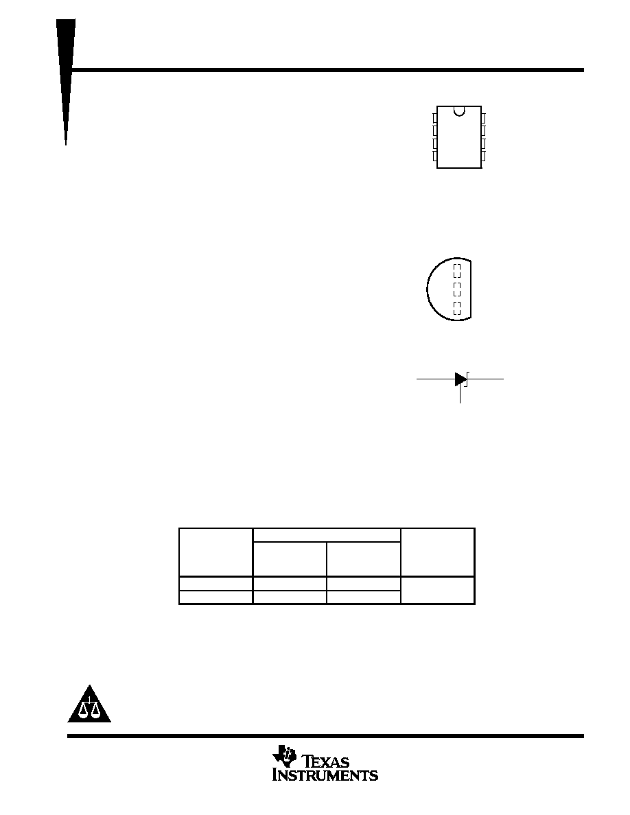
1
2
3
4
8
7
6
5
NC
NC
NC
ANODE
CATHODE
NC
CATHODE
ADJ
D PACKAGE
(TOP VIEW)
NC ≠ No internal connection
ANODE
CATHODE
ADJ
LP PACKAGE
(TOP VIEW)
logic symbol
ANODE
CATHODE
ADJ

LT1009
2.5-V INTEGRATED REFERENCE CIRCUITS
SLVS013G ≠ MAY 1987 ≠ REVISED NOVEMBER 1999
2
POST OFFICE BOX 655303
∑
DALLAS, TEXAS 75265
schematic
Q14
Q11
Q13
Q12
Q9
Q10
Q8
Q7
Q2
Q1
Q3
Q4
Q5
Q6
ANODE
CATHODE
ADJ
30
k
500
720
10
k
20 pF
30 pF
24 k
24 k
6.6 k
6.6 k
All component values shown are nominal.
absolute maximum ratings over operating free-air temperature range
Reverse current, I
R
20 mA
. . . . . . . . . . . . . . . . . . . . . . . . . . . . . . . . . . . . . . . . . . . . . . . . . . . . . . . . . . . . . . . . . . . . . .
Forward current, I
F
10 mA
. . . . . . . . . . . . . . . . . . . . . . . . . . . . . . . . . . . . . . . . . . . . . . . . . . . . . . . . . . . . . . . . . . . . . . .
Package thermal impedance,
JA
, (see Notes 1 and 2): D package
97
∞
C/W
. . . . . . . . . . . . . . . . . . . . . . . . . . . .
LP package
156
∞
C/W
. . . . . . . . . . . . . . . . . . . . . . . . . .
Lead temperature 1,6 mm (1/16 inch) from case for 10 seconds: D and LP packages
260
∞
C
. . . . . . . . . . . . .
Storage temperature range, T
stg
≠ 65
∞
C to 150
∞
C
. . . . . . . . . . . . . . . . . . . . . . . . . . . . . . . . . . . . . . . . . . . . . . . . . . .
Stresses beyond those listed under "absolute maximum ratings" may cause permanent damage to the device. These are stress ratings only, and
functional operation of the device at these or any other conditions beyond those indicated under "recommended operating conditions" is not
implied. Exposure to absolute-maximum-rated conditions for extended periods may affect device reliability.
NOTES:
1. Maximum power dissipation is a function of TJ(max)
,
JA, and TA. The maximum allowable power dissipation at any allowable ambient
temperature is PD = (TJ(max) ≠ TA)/
JA. Operation at the absolute maximum TJ of 150
∞
C can impact reliability.
2. The package thermal impedance is calculated in accordance with JESD 51.
recommended operating conditions
MIN
MAX
UNIT
Operating free air temperature range TA
LT1009C
0
70
∞
C
Operating free-air temperature range, TA
LT1009I
≠40
85
∞
C
LT1009
2.5-V INTEGRATED REFERENCE CIRCUITS
SLVS013G ≠ MAY 1987 ≠ REVISED NOVEMBER 1999
3
POST OFFICE BOX 655303
∑
DALLAS, TEXAS 75265
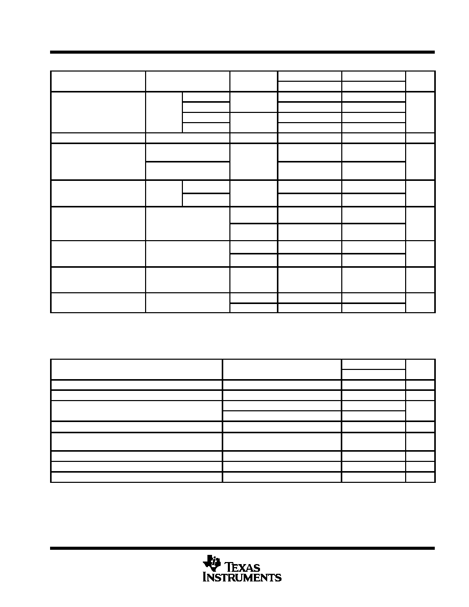
electrical characteristics at specified free-air temperature
PARAMETER
TEST CONDITIONS
T
LT1009C
LT1009I
UNIT
PARAMETER
TEST CONDITIONS
TA
MIN
TYP
MAX
MIN
TYP
MAX
UNIT
D package
25
∞
C
2.49
2.5
2.51
2.49
2.5
2.51
VZ
Reference voltage
IZ = 1 mA
LP package
25
∞
C
2.495
2.5
2.505
2.495
2.5
2.505
V
VZ
Reference voltage
IZ = 1 mA
D package
Full range
2.485
2.515
2.475
2.525
V
LP package
Full range
2.491
2.509
2.48
2.52
VF
Forward voltage
IF = 2 mA
25
∞
C
0.4
1
0.4
1
V
Adjustment range
IZ = 1 mA,
VADJ = GND to VZ
25
∞
C
125
125
mV
Adjustment range
IZ = 1 mA,
VADJ = 0.6 V to VZ ≠ 0.6 V
25
∞
C
45
45
mV
VZ(t
)
Change in
reference voltage
D package
Full range
5
15
mV
VZ(temp) reference voltage
with temperature
LP package
Full range
4
15
mV
VZ
Average
temperature
0
∞
C to 70
∞
C
15
25
30
ppm/
∞
C
VZ
coefficient of
reference voltage
≠ 40
∞
C to 85
∞
C
20
ppm/
∞
C
VZ
Change in
reference voltage
IZ = 400
µ
A to 10 mA
25
∞
C
2.6
10
2.6
6
mV
VZ
reference voltage
with current
IZ = 400
µ
A to 10 mA
Full range
12
10
mV
VZ/
t
Long-term change
in reference
voltage
IZ = 1 mA
25
∞
C
20
20
ppm/khr
z
Reference
IZ = 1 mA
25
∞
C
0.3
1
0.3
1
zz
impedance
IZ = 1 mA
Full range
1.4
1.4
Full range is 0
∞
C to 70
∞
C for the LT1009C and ≠ 40
∞
C to 85
∞
C for the LT1009I.
The average temperature coefficient of reference voltage is defined as the total change in reference voltage divided by the specified temperature
range.
electrical characteristics at T
A
= 25
∞
C
PARAMETER
TEST CONDITIONS
LT1009Y
UNIT
PARAMETER
TEST CONDITIONS
MIN
TYP
MAX
UNIT
VZ
Reference voltage
IZ = 1 mA
2.49
2.5
2.51
V
VF
Forward voltage
IF = 2 mA
0.4
1
V
Adjustment range
IZ = 1 mA,
VADJ = GND to VZ
125
mV
Adjustment range
IZ = 1 mA,
VADJ = 0.6 V to VZ ≠ 0.6 V
45
mV
VZ(temp)
Change in reference voltage with temperature
2.5
mV
VZ
Average temperature coefficient of
reference voltage
15
ppm/
∞
C
VZ
Change in reference voltage with current
IZ = 400
µ
A to 10 mA
2.6
mV
VZ/
t
Long-term change in reference voltage
IZ = 1 mA
20
ppm/khr
zz
Reference impedance
IZ = 1 mA
0.3
1
W
The average temperature coefficient of reference voltage is defined as the total change in reference voltage divided by the specified temperature
range.
LT1009
2.5-V INTEGRATED REFERENCE CIRCUITS
SLVS013G ≠ MAY 1987 ≠ REVISED NOVEMBER 1999
4
POST OFFICE BOX 655303
∑
DALLAS, TEXAS 75265
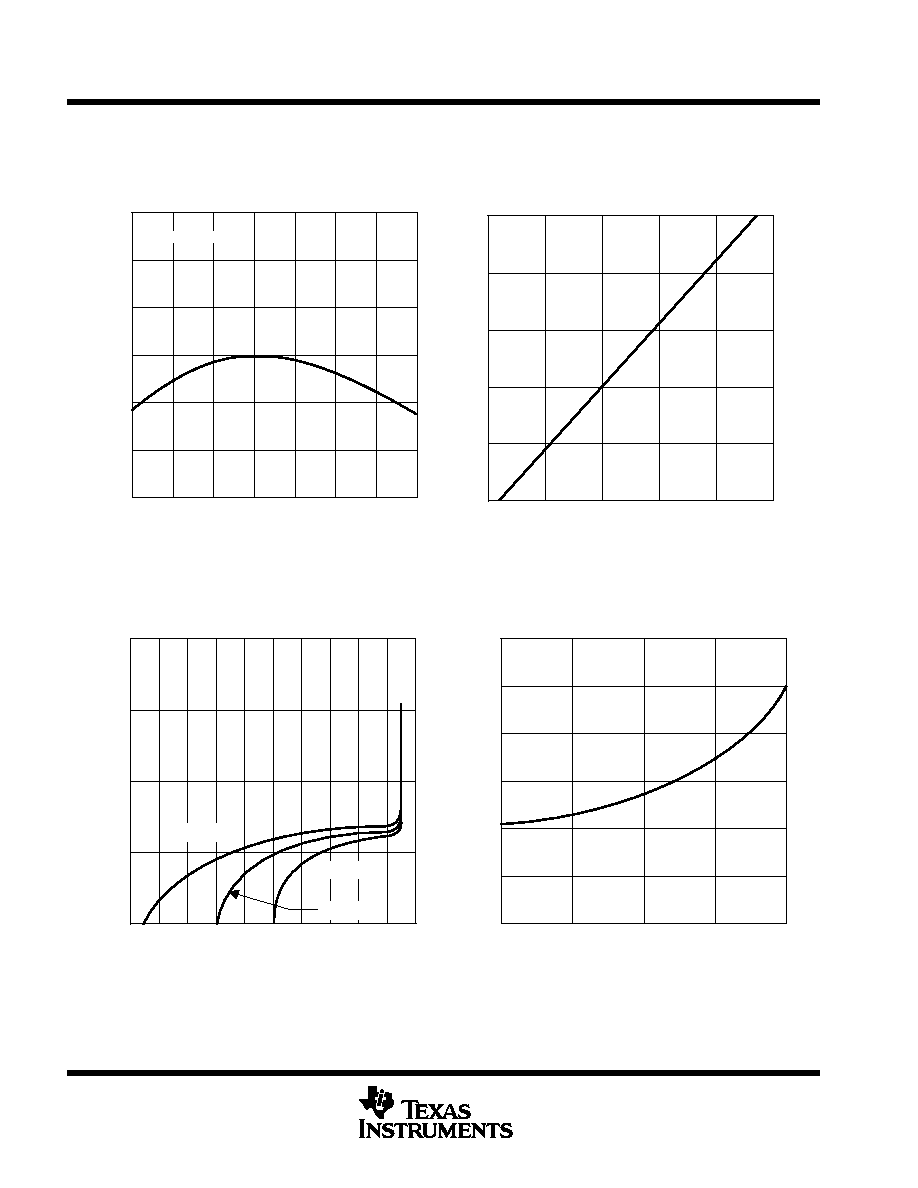
TYPICAL CHARACTERISTICS
Figure 1
V
Z
2.5
2.49
2.48
2.47
≠ 50
≠ 25
0
25
50
75
≠ Reference V
oltage ≠ V
2.51
2.52
REFERENCE VOLTAGE
vs
FREE-AIR TEMPERATURE
2.53
100
125
TA ≠ Free-Air Temperature ≠
∞
C
Iz = 1 mA
Figure 2
V
Z
3
2
1
0
0
4
8
12
16
20
≠ Change in Reference V
oltage ≠ mV
4
5
IZ ≠ Reference Current ≠ mA
CHANGE IN REFERENCE VOLTAGE
vs
REFERENCE CURRENT
Figure 3
I R
0.6
1
1.4
1.8
2.2
2.6
≠ Reverse Current ≠
A
VR ≠ Reverse Voltage ≠ V
10 ≠ 1
TJ = 25
∞
C
TJ = ≠ 55
∞
C
TJ = 125
∞
C
10 ≠ 2
10 ≠ 3
10 ≠ 4
10 ≠ 5
REVERSE CURRENT
vs
REVERSE VOLTAGE
Figure 4
0.6
0.4
0.2
0
0.001
0.01
0.1
1
10
0.8
1
IF ≠ Forward Current≠ mA
1.2
V
F
≠ Forward V
oltage ≠ V
TJ = 25
∞
C
FORWARD VOLTAGE
vs
FORWARD CURRENT
Data at high and low temperatures are applicable only within the rated operating free-air temperature ranges of the various devices.
LT1009
2.5-V INTEGRATED REFERENCE CIRCUITS
SLVS013G ≠ MAY 1987 ≠ REVISED NOVEMBER 1999
5
POST OFFICE BOX 655303
∑
DALLAS, TEXAS 75265
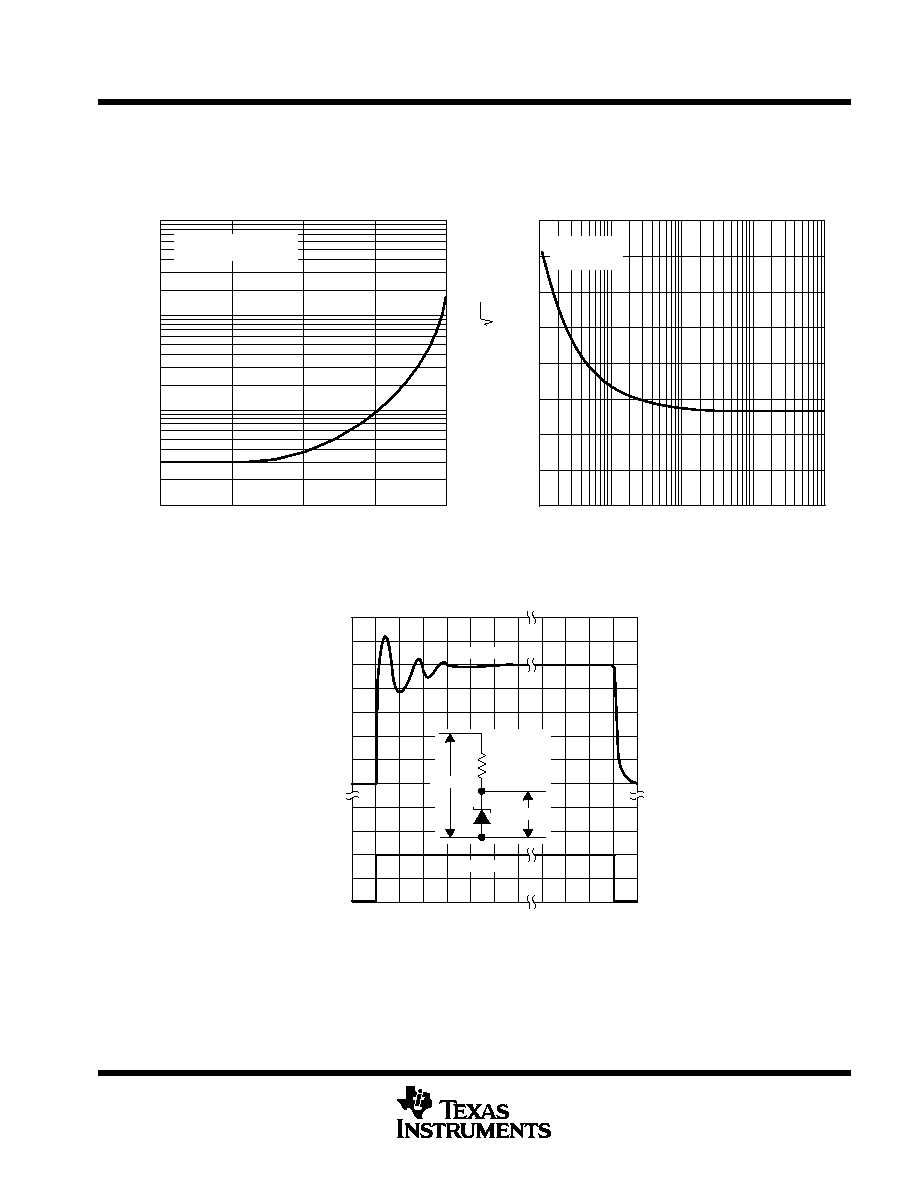
TYPICAL CHARACTERISTICS
Figure 5
1
0.1
0.01
0.1
1
10
100
10
f ≠ Frequency ≠ kHz
REFERENCE IMPEDANCE
vs
FREQUENCY
100
z
z
≠ Reference Impedance ≠
Iz = 1 mA
TJ = ≠ 55
∞
C to 125
∞
C
Figure 6
10
100
1 k
10 k
100 k
f ≠ Frequency ≠ Hz
50
100
150
200
250
NOISE VOLTAGE
vs
FREQUENCY
nV/
Hz
≠ Noise V
oltage ≠
V
n
Iz = 1 mA
TJ = 25
∞
C
Input
Output
5 k
2.5
2
1.5
1
0.5
0
8
4
0
Input and Output V
oltages ≠ V
0
1
20
Input
Output
t ≠ Time ≠
µ
s
TRANSIENT RESPONSE
3
3.5
Figure 7