 | –≠–Ľ–Ķ–ļ—ā—Ä–ĺ–Ĺ–Ĺ—č–Ļ –ļ–ĺ–ľ–Ņ–ĺ–Ĺ–Ķ–Ĺ—ā: OPA561 | –°–ļ–į—á–į—ā—Ć:  PDF PDF  ZIP ZIP |
OPA561
SBOS206A ≠ DECEMBER 2001 ≠ REVISED JUNE 2002
High≠Current, High≠Speed
OPERATIONAL AMPLIFIER
1
www.ti.com
FEATURES
D
1.2A OUTPUT CURRENT
D
12Vp≠p OUTPUT VOLTAGE
D
WIDE POWER RANGE:
Single Supply: +7V to +15V
Dual Supply:
Ī
3.5V to
Ī
7.5V
D
FULLY PROTECTED:
Thermal Shutdown
Adjustable Current Limit
D
OUTPUT DISABLE CONTROL
D
17MHz GAIN≠BANDWIDTH PRODUCT
D
50V/
Ķ
s SLEW RATE
D
1MHz FULL≠POWER BANDWIDTH
D
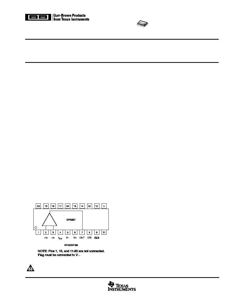
THERMALLY ENHANCED HTSSOP≠20
PowerPAD PACKAGE
APPLICATIONS
D
POWER≠LINE COMMUNICATIONS
D
VALVE≠ACCUATOR DRIVERS
D
POWER SUPPLIES
D
TEST EQUIPMENT
D
TEC DRIVERS
D
LASER DIODE DRIVERS
DESCRIPTION
The OPA561 is a low≠cost, high≠current operational
amplifier capable of driving up to 1.2A pulses into reactive
loads. This monolithic integrated circuit provides high
reliability in demanding line≠carrier communications, laser
diode drivers, and motor control applications. The high
slew rate provides 1MHz full≠power bandwidth and
excellent linearity.
The OPA561 operates from either a single supply in the
range of 7V to 15V or dual power supplies of
Ī
3.5V to
Ī
7.5V for design flexibility. In single≠supply operation, the
input common≠mode range extends below ground. At
maximum output current, a wide output swing provides a
12Vp≠p capability with a nominal 15V supply.
The OPA561 is internally protected against over≠tempera-
ture conditions and current overloads. In addition, the
OPA561 is designed to provide an accurate, user≠se-
lected, current limit. The current limit can be adjusted from
0.2A to 1.2A with a low≠power resistor/potentiometer or
DAC (Digital≠to≠Analog Converter). The high≠speed
characteristics of the current control loop provide accuracy
even under pulsed load conditions.
The Enable/Status (E/S) pin performs two functions: it can
be monitored to determine if the device is in thermal
shutdown (active LOW), and it can also be forced LOW to
disable the output, disconnecting the load.
The OPA561 is available in the miniature, HTSSOP≠20
PowerPAD
, power package. This surface≠mount
package is thermally enhanced and has a very low thermal
resistance. Operation is specified over the extended
industrial temperature range, ≠40
_
C to +125
_
C.
PowerPAD is a registered trademark of Texas Instruments Incorporated
.
Copyright
2001, Texas Instruments Incorporated
PRODUCTION DATA information is current as of publication date.
Products conform to specifications per the terms of Texas Instruments
standard warranty. Production processing does not necessarily include
testing of all parameters.
Please be aware that an important notice concerning availability, standard warranty, and use in critical applications of Texas Instruments
semiconductor products and disclaimers thereto appears at the end of this data sheet.
OPA561
SBOS206A ≠ DECEMBER 2001 ≠ REVISED JUNE 2002
2
www.ti.com
ABSOLUTE MAXIMUM RATINGS
(1)
Supply Voltage, V≠ to V+
16V
. . . . . . . . . . . . . . . . . . . . . . . . . . .
Input Voltage Range
(V≠) ≠ 0.4V to (V+) + 0.5V
. . . . . . . . . . . . . . . .
Input Shutdown Voltage
(V≠) ≠ 0.4V to (V≠) + 5.0V
. . . . . . . . . . . . . .
Operating Temperature
≠40
į
C to +125
į
C
. . . . . . . . . . . . . . . . . . . .
Storage Temperature
≠65
į
C to +150
į
C
. . . . . . . . . . . . . . . . . . . . .
Junction Temperature
150
į
C
. . . . . . . . . . . . . . . . . . . . . . . . . . . .
Lead Temperature (soldering, 10s)
300
į
C
. . . . . . . . . . . . . . . . . . . .
NOTE: (1) Stresses above these ratings may cause permanent damage.
Exposure to absolute maximum conditions for extended periods may degrade
device reliability. These are stress ratings only, and functional operation of the
device at these or any other conditions beyond those specified is not implied.
ELECTROSTATIC
DISCHARGE SENSITIVITY
This integrated circuit can be damaged by ESD. Texas
Instruments recommends that all integrated circuits be
handled with appropriate precautions. Failure to ob-
serve proper handling and installation procedures can
cause damage.
ESD damage can range from subtle performance
degradation to complete device failure. Precision
integrated circuits may be more susceptible to damage
because very small parametric changes could cause
the device not to meet its published specifications.
PACKAGE/ORDERING INFORMATION
PRODUCT
PACKAGE≠LEAD
PACKAGE
DESIGNATOR(1)
SPECIFIED
TEMPERATURE
RANGE
PACKAGE
MARKING
ORDERING
NUMBER
TRANSPORT
MEDIA, QUANTITY
OPA561PWP
HTSSOP 20
PWP
40
į
C to +125
į
C
OPA561
OPA561PWP
Rail, 70
OPA561PWP
HTSSOP≠20
PWP
≠40
į
C to +125
į
C
OPA561
OPA561PWP/2K
Tape and Reel, 2000
NOTE: (1) For the most current specification and package information, refer to our web site at www.ti.com.
ELECTRICAL CHARACTERISTICS
BOLDFACE limits apply over the specified temperature range, T
A
= ≠40
į
C to +125
į
C
At TCASE = +25
į
C, VS = 15V, load connected to VS/2, and E/S enabled, unless otherwise noted.
OPA561PWP
PARAMETER
CONDITIONS
MIN
TYP
MAX
UNITS
OFFSET VOLTAGE
VS = 12V
Input Offset Voltage
VOS
VCM = 0V
Ī
1
Ī
20
mV
vs Temperature
dVOS/dT
Ī
50
Ķ
V/
į
C
vs Power Supply
PSRR
VCM = 0V, VS = 7V to 16V
25
150
Ķ
V/V
INPUT BIAS CURRENT(1)
Input Bias Current
IB
VCM = 0V
10
100
pA
Input Offset Current
IOS
VCM = 0V
10
100
pA
NOISE
Input Voltage Noise Density
en
f = 1kHz
83
nV/
Hz
f = 10kHz
32
nV/
Hz
f = 100kHz
14
nV/
Hz
Current Noise
in
f = 1kHz
4
fA/
Hz
INPUT VOLTAGE RANGE
Common≠Mode Voltage Range
VCM
Linear Operation
(V≠) ≠ 0.1
(V+) ≠ 3
V
Common≠Mode Rejection Ratio
CMRR VS = 15V, VCM = (V≠) ≠ 0.1V to (V+) ≠ 3V
70
80
dB
INPUT IMPEDANCE
Differential
1.8
S
1011 || 10
|| pF
Common≠Mode
1.8
S
1011 || 18.5
|| pF
OPEN≠LOOP GAIN
Open≠Loop Voltage Gain
AOL
VO = 10Vp≠p, RL = 5
80
100
dB
FREQUENCY RESPONSE
Gain≠Bandwidth Product
GBW
RL = 5
17
MHz
Slew Rate
SR
G = 1, 10V Step, RL = 5
50
V/
Ķ
s
Full≠Power Bandwidth
G = +2, VOUT = 10Vp≠p
1
MHz
Settling Time:
Ī
0.1%
G = ≠1, 10V Step
1
Ķ
s
Total Harmonic Distortion + Noise
THD+N
f = 1kHz, RL = 5
, G = +2, VO = 10Vp≠p
0.02
%
f = 1MHz
3
%

OPA561
SBOS206A ≠ DECEMBER 2001 ≠ REVISED JUNE 2002
3
www.ti.com
ELECTRICAL CHARACTERISTICS
(Cont.)
BOLDFACE limits apply over the specified temperature range, T
A
= ≠40
į
C to +125
į
C
At TCASE = +25
į
C, VS = 15V, load connected to VS/2, and E/S enabled, unless otherwise noted.
OPA561PWP
PARAMETER
CONDITIONS
MIN
TYP
MAX
UNITS
OUTPUT
Voltage Output, Positive
IO = 0.5A
(V+) ≠ 1
(V+) ≠ 0.7
V
Negative
IO = ≠0.5A
(V≠) + 1
(V≠) + 0.7
V
Positive
IO = 1A
(V+) ≠ 1.5
(V+) ≠ 1.2
V
Negative
IO = ≠1A
(V≠) + 1.5
(V≠) + 1.2
V
Maximum Continuous Current Output, dc
1.2
A
Output Impedance
ZO
G = +2, f = 100kHz
0.05
Ouput Current Limit Range
Ī
0.2 to
Ī
1.2
A
Current Limit Tolerance(2)
RCL = 2k
(ILIM =
Ī
1A)
Ī
50
mA
Asymmetry
Comparing Positive and Negative Limits
10
%
Current Limit Overshoot(3)
V = 5V Pulse (200ns tr), G = +2
50
%
Output Disabled
Output Resistance
10
M
Output Capacitance
140
pF
OUTPUT ENABLE/STATUS AND FLAG PINS
Shutdown Input Mode
VE/S HIGH (output enabled)(4)
E/S Pin Open or Forced HIGH
(V≠) + 2
(V≠) + 5
V
VE/S LOW (output disabled)
E/S Pin Forced LOW
(V≠) ≠ 0.4
(V≠) + 0.8
V
IE/S HIGH (output enabled)
E/S Pin Indicates HIGH
20
Ķ
A
IE/S LOW (output disabled)
E/S Pin Indicates LOW
0.1
Ķ
A
Output Disable Time
50
ns
Output Enable Time
3
Ķ
s
Thermal Shutdown Status
Normal Operation
Sourcing 20
Ķ
A
(V≠) + 2
V
Thermally Shutdown
(V≠) + 0.8
V
Current Limit Status
Normal Operation
Sourcing 20
Ķ
A
(V≠) + 0.8
V
Current Limit Flagged
(V≠) + 2
V
Junction Temperature at Shutdown
160
į
C
Reset Temperature from Shutdown
140
į
C
POWER SUPPLY
Specified Voltage
VS
15
V
Operating Voltage Range, (V+) ≠ (V≠)
7
16
V
Quiescent Current
IQ
ILIM Connected to V≠, IQ = 0
50
60
mA
vs Temperature
60
70
mA
Quiescent Current in Shutdown Mode
ILIM Connected to V≠
250
Ķ
A
TEMPERATURE RANGE
Specified Junction Temperature Range
≠40
+125
į
C
Storage Range
≠65
+150
į
C
Thermal Resistance
HTSSOP≠20 PowerPAD
JC
1.4
į
C/W
JA
2oz. Trace and 9in2 Copper Pad with Solder
32
į
C/W
JA
Without Heatsink
100
į
C/W
NOTES: (1) High≠speed test at TJ = +25
į
C. (2) See text for more information on on current limit accuracy. (3) Transient load transition time must be
200ns. (4) 402k
pull≠up resistor to V+ can be used to permanently enable the OPA561.
OPA561
SBOS206A ≠ DECEMBER 2001 ≠ REVISED JUNE 2002
4
www.ti.com
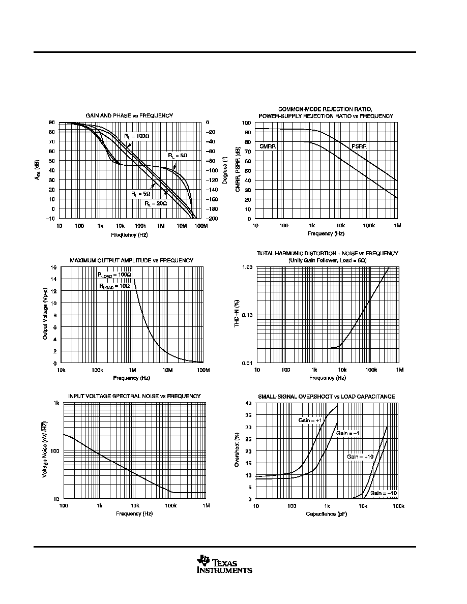
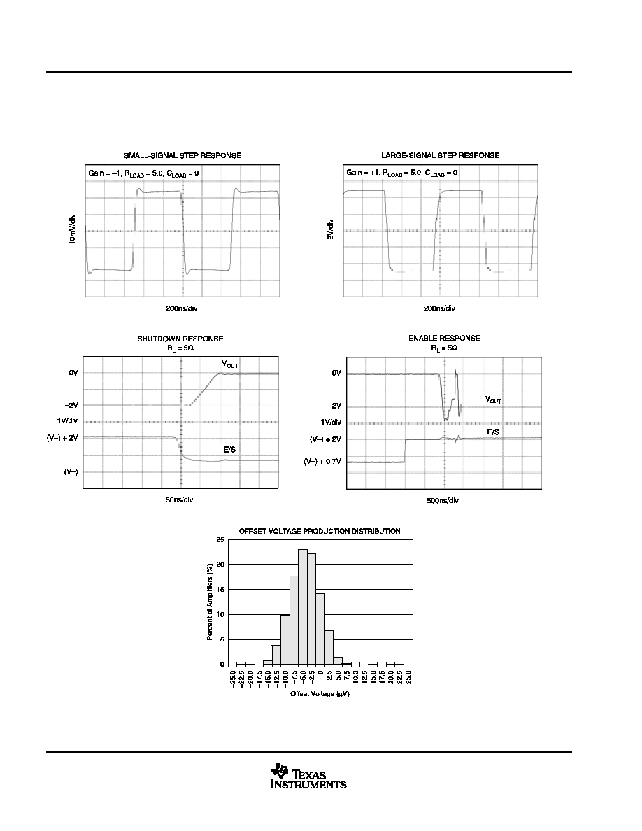
TYPICAL CHARACTERISTICS
At TCASE = +25
į
C, VS = 15V, and enabled, unless otherwise noted.

OPA561
SBOS206A ≠ DECEMBER 2001 ≠ REVISED JUNE 2002
5
www.ti.com
TYPICAL CHARACTERISTICS (Cont.)
At TCASE = +25
į
C, VS = 15V, and E/S enabled, unless otherwise noted.
OPA561
SBOS206A ≠ DECEMBER 2001 ≠ REVISED JUNE 2002
6
www.ti.com
TYPICAL CHARACTERISTICS (Cont.)
At TCASE = +25
į
C, VS = 15V, and E/S enabled, unless otherwise noted.
OPA561
SBOS206A ≠ DECEMBER 2001 ≠ REVISED JUNE 2002
7
www.ti.com
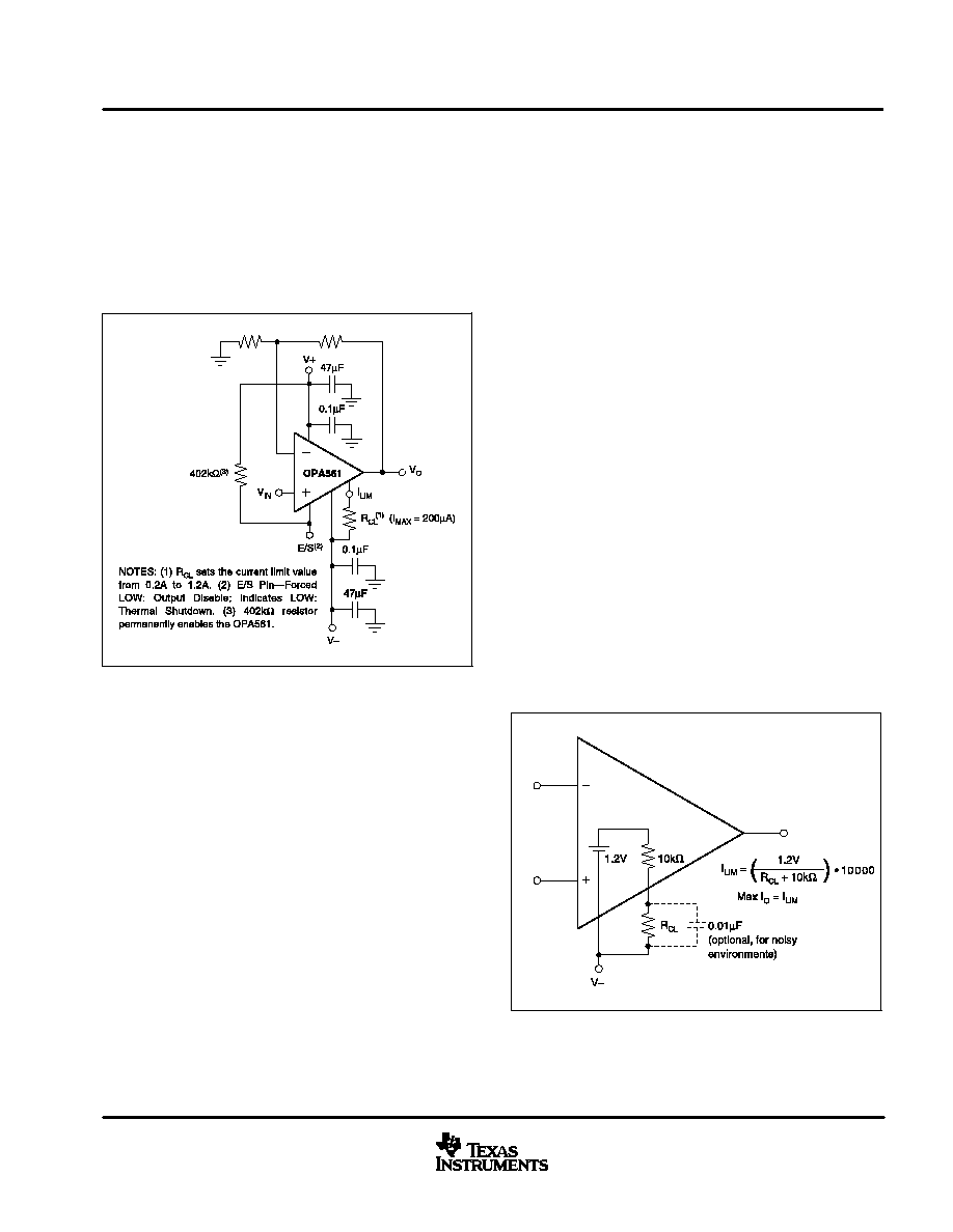
APPLICATIONS INFORMATION
Figure 1 shows the OPA561 connected as a basic
noninverting amplifier. However, the OPA561 can be
used in virtually any op amp configuration.
Power≠supply terminals should be bypassed with low
series impedance capacitors. The technique of using a
ceramic and tantalum type in parallel is recommended.
Power≠supply wiring should have low series impedance.
FIGURE 1. Basic Circuit Connections.
POWER SUPPLIES
The OPA561 operates from single (+7V to +15V) or
dual (
Ī
3.5V to
Ī
7.5V) supplies with excellent
performance. Power≠supply voltages do not need to
be equal. For example, the positive supply could be
set to 10V with the negative supply at ≠5V, or
vice≠versa. Most behaviors remain unchanged
throughout the operating voltage range. Parameters
that vary significantly with operating voltage are
shown in the typical characteristics.
ADJUSTABLE CURRENT LIMIT
The OPA561's accurate, user≠defined, current limit can
be set from 0.2A to 1.2A by controlling the input to the I
LIM
pin. Unlike other designs that use a power resistor in
series with the output current path, the OPA561 senses
the load internally. This allows the current limit to be set
with low≠power components. In contrast, other designs
require one or two expensive power resistors that can
handle the full output current (1.2A in this case).
Current Limit Accuracy
Separate circuits monitor the positive and negative
currents. Each output is compared to a single internal
reference that is set by the external current limit resistor
(or voltage). The OPA561 employs a patented circuit
technique to achieve an accurate and stable current
limit. The output current limit has an accuracy of up to
5% on the 1A current limit. Due to internal matching
limitations, the positive and negative current limits can
be slightly different. However, the values are typically
within 10% of each other.
Setting the Current Limit
Leaving the I
LIM
pin open could damage the part.
Connecting I
LIM
directly to V≠ programs the maximum
output current limit, typically 1.2A. The simplest method
for adjusting the current limit (I
LIM
) uses a resistor or
potentiometer connected between the I
LIM
pin and V≠
according to Equation 1:
I
LIM
= (1.2V/(R
CL
+ 10k
))
∑
10000
(1)
This external resistor determines a small internal
current which sets the desired output current limit.
Alternatively, the output current limit can be set by
applying a voltage to the I
LIM
pin. Figure 2 shows a
simplified schematic of the OPA561's current limit.
FIGURE 2. Adjustable Current Limit--Resistor Method.

OPA561
SBOS206A ≠ DECEMBER 2001 ≠ REVISED JUNE 2002
8
www.ti.com
ENABLE/STATUS (E/S) PIN
The Enable/Status Pin provides two unique functions: 1)
output disable by forcing the pin "LOW" and 2) thermal
shutdown indication by monitoring the voltage level at
the pin. One or both of these functions can be utilized on
the same device. For normal operation (output enabled),
the E/S pin must be pulled "HIGH" (at least 2V above V≠).
A small value capacitor connected between the E/S pin
and V≠ may be appropriate for noisy applications. To
enable the OPA561 permanently, the E/S pin can be tied
to V+ through a 402k
pull≠up resistor.
Output Disable
The shutdown pin is referenced to the negative supply
(V≠). Therefore, shutdown operation is slightly different
in single≠supply and dual≠supply applications.
In single≠supply operation, V≠ typically equals common
ground. Therefore, the shutdown logic signal and the
OPA561's shutdown pin are referenced to the same
potential. In this configuration, the logic pin and the
OPA561 enable can simply be tied together. Shutdown
occurs for voltage levels of < 0.8V. The OPA561 is
enabled at logic levels > 2V.
In dual≠supply operation, the logic pin is still referenced to
a logic ground. However, the shutdown pin of the OPA561
is still referenced to V≠. To shutdown the OPA561, the
voltage level of the logic signal needs to be level shifted
using an optocoupler, as shown in Figure 3.
FIGURE 3. OPA561 Shutdown Configuration for Dual
Supplies.
To disable the output, the E/S pin is pulled "LOW", no
greater than 0.8V above V≠. This function can be used
to conserve power during idle periods. The typical time
required to shut down the output is 50ns. To return the
output to an enabled state, the E/S pin should be pulled
to at least 2.0V above V≠. Typically, the output is
enabled within 3
Ķ
s. It should be noted that pulling the
E/S pin HIGH (output enabled) does not disable the
internal thermal shutdown.
Ensuring Microcontroller Compatibility
Not all microcontrollers output the same logic state after
power≠up or reset. 8051≠type microcontrollers, for
example, output logic HIGH levels on their ports while
other models power up with logic LOW levels after
reset.
In configuration (a) as shown in Figure 3, the shutdown
signal is applied on the cathode side of the photodiode
within the optocoupler. A high logic level causes the
OPA561 to be enabled, and a low logic level shuts the
OPA561 down. In configuration (b) of Figure 3, with the
logic signal applied on the anode side, a high level
causes the OPA561 to shutdown and low level enables
the op amp.
OVER≠CURRENT FLAG
The OPA561 features an over≠current status flag (CLS,
Pin 9) that can be monitored to see if the load exceeds
the current limit. The output signal of the over current
limit flag is compatible to standard logic. The CLS signal
is referenced to V≠. A voltage level of less than (V≠) +
0.8V indicates normal operation and a level of greater
than (V≠) + 2 indicates that the OPA561 is in current
limit. The flag is HIGH as long as the output of the
OPA561 is in current limit. At very low signal
frequencies, typically < 1kHz, both the upper (sourcing
current) and lower current limit (sinking current) are
monitored. At frequencies > 1kHz, due to internal circuit
limitations, the flag output signal for the upper current
limit becomes delayed and shortened. The flag signal
for the lower current limit is unaffected by this behavior.
As the signal frequency increases further, only the lower
current limit (sinking current) is output on Pin 9.
OUTPUT STAGE COMPENSATION
The complex load impedances common in power op amp
applications can cause output stage instability. For normal
operation, output compensation circuitry is typically not
required. However, if the OPA561 is intended to be driven
into current limit, an R/C network (snubber) may be
required. A snubber circuit may also enhance stability
when driving large capacitive loads ( > 1000pF) or
inductive loads (motors, loads separated from the
amplifier by long cables). Typically, 3
to 10
in series
with 0.01
Ķ
F to 0.1
Ķ
F is adequate. Some variations in
circuit value may be required with certain loads.
OPA561
SBOS206A ≠ DECEMBER 2001 ≠ REVISED JUNE 2002
9
www.ti.com
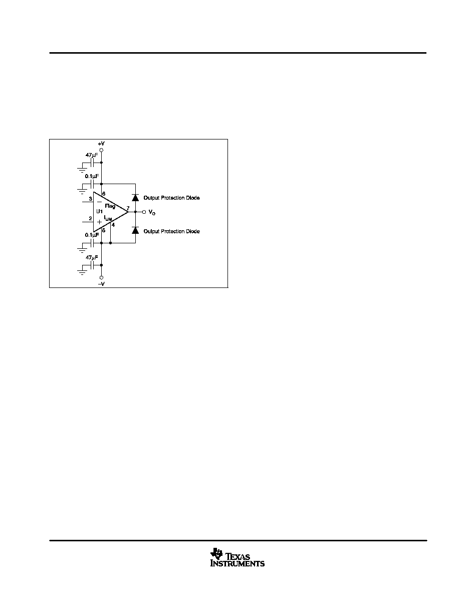
OUTPUT PROTECTION
Reactive and EMF≠generation loads can return load
current to the amplifier, causing the output voltage to
exceed the power≠supply voltage. This damaging
condition can be avoided with clamp diodes from the output
terminal to the power supplies, as shown in Figure 4.
Schottky rectifier diodes with a 3A or greater continuous
rating are recommended.
FIGURE 4. Output Protection Diode.
THERMAL PROTECTION
The OPA561 has thermal sensing circuitry that helps
protect the amplifier from exceeding temperature limits.
Power dissipated in the OPA561 will cause the junction
temperature to rise. Internal thermal shutdown circuitry
shuts down the output when the die temperature reaches
approximately 160
į
C, resetting when the die has cooled
to 140
į
C. Depending on load and signal conditions, the
thermal protection circuit may cycle on and off. This limits
the dissipation of the amplifier, but may have an
undesirable effect on the load. Any tendency to activate
the thermal protection circuit indicates excessive power
dissipation or an inadequate heatsink. For reliable,
long≠term, continuous operation, junction temperature
should be limited to 125
į
C, maximum. To estimate the
margin of safety in a complete design (including
heatsink), increase the ambient temperature until the
thermal protection is triggered. Use worst≠case loading
and signal conditions. For good, long≠term reliability,
thermal protection should trigger more than 35
į
C above
the maximum expected ambient condition of your
application. This produces a junction temperature of
125
į
C at the maximum expected ambient condition.
The internal protection circuitry of the OPA561 was
designed to protect against overload conditions; it was
not intended to replace proper heatsinking.
Continuously running the OPA561 into thermal
shutdown can degrade reliability. The E/S pin can be
monitored to determine if shutdown has occurred.
During normal operation the voltage on the E/S pin is
typically above (V≠) + 2V. During shutdown, the voltage
drops to less than (V≠) + 0.8V.
POWER DISSIPATION
Power dissipation depends on power supply, signal,
and load conditions. For DC signals, power dissipation
is equal to the product of output current times the
voltage across the conducting output transistor.
Dissipation with ac signals is lower. Application Bulletin
AB≠039 (SBOA022) explains how to calculate or
measure power dissipation with unusual signals and
loads and can be found at www.ti.com.
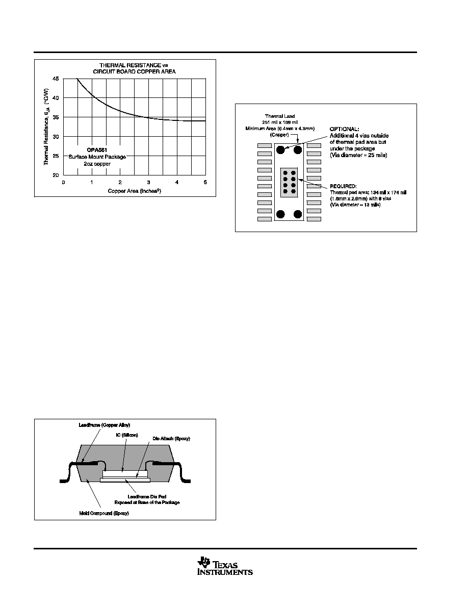
HEATSINK AREA
The relationship between thermal resistance and power
dissipation can be expressed as:
JA
=
T
J
≠
T
A
/
P
D
where T
J
= Junction Temperature (
į
C)
T
A
= Ambient Temperature (
į
C)
JA
= Junction to Ambient Thermal Resistance (
į
C/W)
P
D
= Power Dissipation (W)
To appropriately determine required heatsink area,
required power dissipation should be calculated and the
relationship between power dissipation and thermal
resistance should be considered to minimize shutdown
conditions and allow for proper long≠term operation
(junction temperature of 125
į
C). Once the heatsink
area has been selected, worst≠case load conditions
should be tested to ensure proper thermal protection.
For applications with limited board size, refer to Figure 5
for the approximate thermal resistance relative to
heatsink area. Increasing heatsink area beyond 2in
2
provides little improvement in thermal resistance. To
achieve the 32
į
C/W stated in the Electrical
Characteristics, a copper plane size of 9in
2
was used.
The HTSSOP≠20 PowerPAD package is well suited for
continuous power levels from 2W to 4W, depending on
ambient temperature and heatsink area. Higher power
levels may be achieved in applications with a low on/off
duty cycle, such as remote meter reading.
OPA561
SBOS206A ≠ DECEMBER 2001 ≠ REVISED JUNE 2002
10
www.ti.com
FIGURE 5. Thermal Resistance vs Circuit Board
Copper Area.
AMPLIFIER MOUNTING
What is PowerPAD?
The OPA561 uses the HTSSOP≠20 PowerPAD
package, a thermally enhanced, standard size IC
package designed to eliminate the use of bulky heatsinks
and slugs traditionally used in thermal packages. This
package can be easily mounted using standard PCB
assembly techniques, and can be removed and replaced
using standard repair procedures.
The PowerPAD package is designed so that the
leadframe die pad (or thermal pad) is exposed on the
bottom of the IC, as shown in Figure 6. This provides an
extremely low thermal resistance (
JC
) path between
the die and the exterior of the package. The thermal pad
on the bottom of the IC can then be soldered directly to
the PCB, using the PCB as a heatsink. In addition,
through the use of thermal vias, the thermal pad can be
directly connected to a ground plane or special heatsink
structure designed into the PCB.
FIGURE 6. Section View of a PowerPAD Package.
PowerPAD Assembly Process
1. Prepare the PCB with a top side etch pattern, as
shown in Figure 7. There should be etch for the leads as
well as etch for the thermal land.
FIGURE 7. 20≠Pin PWP PowerPAD PCB Etch and Via
Pattern.
2. Place the recommended number of holes (or thermal
vias) in the area of the thermal pad. These holes should
be 13 mils in diameter. They are kept small so that solder
wicking through the holes is not a problem during reflow.
The recommended number of holes for the HTSSOP≠20
PowerPAD package is eight, as shown in Figure 7.
3. It is recommended, but not required, to place a small
number of the holes under the package and outside the
thermal pad area. These holes provide additional heat
path between the copper land and ground plane and are
25 mils in diameter. They may be larger because they are
not in the area to be soldered, so wicking is not a
problem. This is illustrated in Figure 7.
4. Connect all holes, including those within the thermal
pad area and outside the pad area, to the internal ground
plane or other internal copper plane.
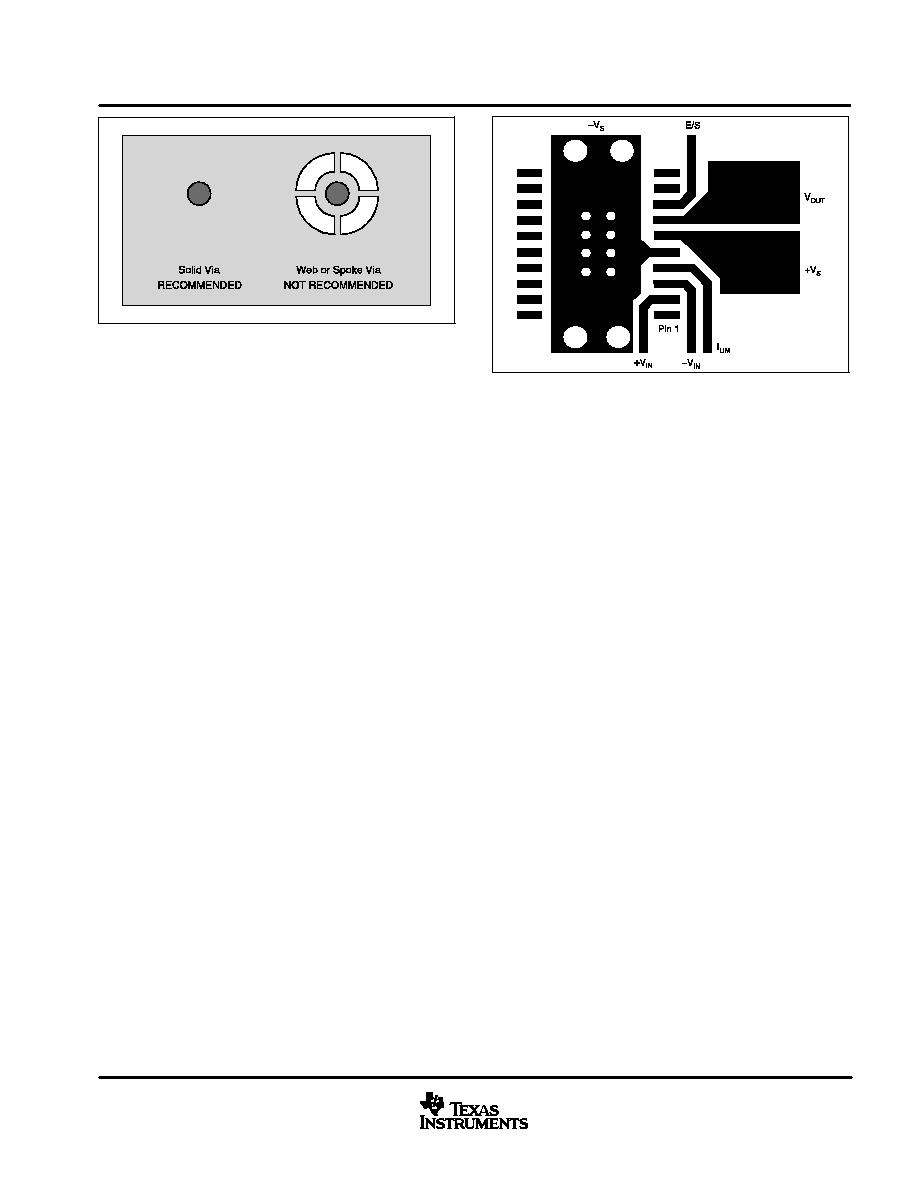
5. When connecting these holes to the ground plane, do
not use the typical web or spoke via connection
methodology, see Figure 8. Web connections have a
high thermal resistance connection that is useful for
slowing the heat transfer during soldering operations.
This makes the soldering of vias that have plane
connections easier. However, in this application, low
thermal resistance is desired for the most efficient heat
transfer. Therefore, the holes under the PowerPAD
package should make their connection to the internal
ground plane with a complete connection around the
entire circumference of the plated through hole.
OPA561
SBOS206A ≠ DECEMBER 2001 ≠ REVISED JUNE 2002
11
www.ti.com
FIGURE 8. Via Connection.
6. The top≠side solder mask should leave exposed the ter-
minals of the package and the thermal pad area. The ther-
mal pad area should leave the 13 mil holes exposed. The
larger 25 mil holes outside the thermal pad area should be
covered with solder mask.
7. Apply solder paste to the exposed thermal pad area and
all of the package terminals.
8. With these preparatory steps in place, the PowerPAD IC
is simply placed in position and run through the solder re-
flow operation as any standard surface≠mount component.
This results in a part that is properly installed.
For detailed information on the PowerPAD package includ-
ing thermal modeling considerations and repair proce-
dures, please see Technical Brief SLMA002, PowerPAD
Thermally Enhanced Package located at www.ti.com.
LAYOUT GUIDELINES
The OPA561 is a high≠speed power amplifier that
requires proper layout for best performance. Figure 9
shows an example of proper layout.
Keep power≠supply leads as short as possible. This will
keep inductance low and resistive losses at a minimum. A
minimum 18 gauge wire thickness is recommended for
power≠supply leads. The wire length should be < 8 inches.
FIGURE 9. OPA561 Example Layout.
Proper power≠supply bypassing with low ESR capacitors
is essential to achieve good performance. A parallel
combination of small ceramic (around 100nF) and bigger
(47
Ķ
F) non≠ceramic bypass capacitors will provide low
impedance over a wide frequency range. Bypass
capacitors should be placed as close as practical to the
power≠supply pins of the OPA561.
PCB traces conducting high currents, such as from
output to load or from the power≠supply connector to
the power≠supply pins of the OPA561 should be kept as
wide and as short as possible. This will keep inductance
low and also resistive losses to a minimum.
The eight holes in the landing pattern for the OPA561
are for the thermal vias that connect the PowerPad of
the OPA561 to the heatsink area on the printed circuit
board. The additional four larger vias further enhance
the heat conduction into the heatsink area. All traces
conducting high currents are very wide for lowest
inductance and minimal resistive losses. Note that the
negative supply (≠V
S
) pin on the OPA561 is connected
through the PowerPad. This allows for maximum trace
width for V
OUT
and the positive power supply (+V
S
).
OPA561
SBOS206A ≠ DECEMBER 2001 ≠ REVISED JUNE 2002
12
www.ti.com
APPLICATIONS CIRCUITS
The high output current and low supply of the OPA561
makes it a good candidate for driving laser diodes and
thermo electric coolers. Figure 10 shows the OPA561
configured as a laser diode driver.
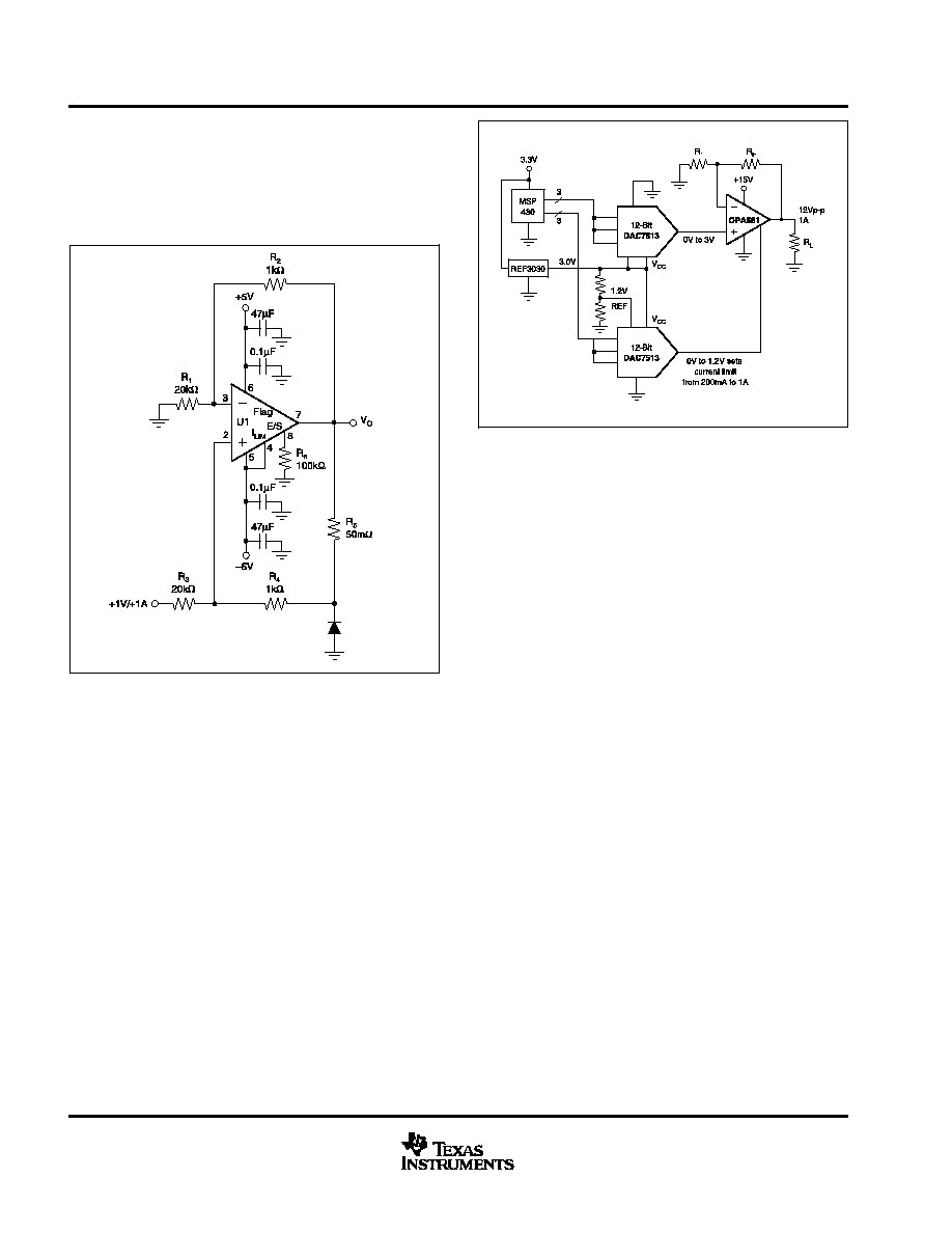
FIGURE 10. Laser Diode Driver.
PROGRAMMABLE POWER SUPPLY
Figure 11 shows the OPA561 configured with the
MSP430, REF3030, and DAC7513 as a space≠saving,
low≠cost, programmable power≠supply solution. This
solution features low≠voltage operation, small≠size
packages, (DAC7513 in SOT23≠8, REF3030 in
SOT23≠3) and low cost (under $10 for complete solution).
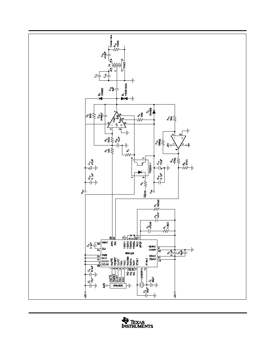
POWER≠LINE COMMUNICATION MODEM
The OPA561 is well suited to drive AC power lines for
low≠speed communications applications. It provides an
easily implemented, reliable solution that is superior to
discrete power transistor circuits. Advantages include:
S
Fully Integrated Solution
S
Integrated Shutdown Circuitry for Send≠and≠Receive Switching
S
Thermal Shutdown
FIGURE 11. Programmable Power Supply.
S
Adjustable Current Limit
S
Shutdown Flag
S
Power Savings
S
Small PowerPAD package
Typically such a system consists of a microcontroller, a
modem IC and the power line interface circuitry. See
Figure 12 for the half≠duplex power line communication
system.
It uses a, synchronous FSK≠modem, capable of 600
and 1200≠baud data rates and supports two different
FSK channels in the 60kHz to 80kHz range. A
microcontroller such as the MSP430 is used to control
the modem IC.
The OPA561 analog interface circuitry drives the FSK
modem signals on the AC power line. It filters the
transmit signal (ATO) from the ST7536 to suppress the
2nd≠harmonic distortion of the transmit signal. It also
amplifies the ATO signal and provides the very low
output impedance necessary to properly drive the line.
The impedance of a typical power line at 70kHz ranges
from 1
to 100
. The OPA561 is ideal for this type of
load. The transformer provides isolation and additional
filtering. C
9
prevents 50/60Hz current from flowing in the
transformer. This capacitor must be chosen carefully for
proper voltage rating and safety characteristics.
The receive input signal is amplified (G = 100) and
applied to the modem IC. The OPA561 is disabled in
receive mode to avoid loading the line.
OPA561
SBOS206A ≠ DECEMBER 2001 ≠ REVISED JUNE 2002
13
www.ti.com
FIGURE 13. Power Line Communication Driver.
OPA561
SBOS206A ≠ DECEMBER 2001 ≠ REVISED JUNE 2002
14
www.ti.com
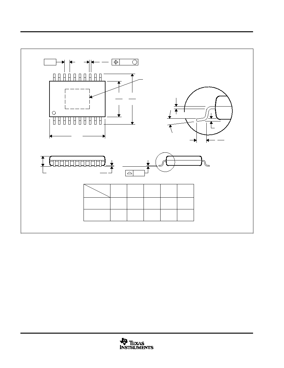
PWP (R-PDSO-G**)
PowerPAD
PLASTIC SMALL-OUTLINE
4073225/F 10/98
0,50
0,75
0,25
0,15 NOM
Thermal Pad
(See Note D)
Gage Plane
28
24
7,70
7,90
20
6,40
6,60
9,60
9,80
6,60
6,20
11
0,19
4,50
4,30
10
0,15
20
A
1
0,30
1,20 MAX
16
14
5,10
4,90
PINS **
4,90
5,10
DIM
A MIN
A MAX
0,05
Seating Plane
0,65
0,10
M
0,10
0
į
≠8
į
20 PINS SHOWN
NOTES: A. All linear dimensions are in millimeters.
B. This drawing is subject to change without notice.
C. Body dimensions do not include mold flash or protrusions.
D. The package thermal performance may be enhanced by bonding the thermal pad to an external thermal plane.
This pad is electrically and thermally connected to the backside of the die and possibly selected leads.
E. Falls within JEDEC MO-153
PowerPAD is a trademark of Texas Instruments Incorporated.

PACKAGING INFORMATION
ORDERABLE DEVICE
STATUS(1)
PACKAGE TYPE
PACKAGE DRAWING
PINS
PACKAGE QTY
OPA561PWP
ACTIVE
HTSSOP
PWP
20
78
OPA561PWP/2K
ACTIVE
HTSSOP
PWP
20
2000
(1) The marketing status values are defined as follows:
ACTIVE: Product device recommended for new designs.
LIFEBUY: TI has announced that the device will be discontinued, and a lifetime-buy period is in effect.
NRND: Not recommended for new designs. Device is in production to support existing customers, but TI does not recommend using this part in
a new design.
PREVIEW: Device has been announced but is not in production. Samples may or may not be available.
OBSOLETE: TI has discontinued the production of the device.
PACKAGE OPTION ADDENDUM
www.ti.com
3-Oct-2003

IMPORTANT NOTICE
Texas Instruments Incorporated and its subsidiaries (TI) reserve the right to make corrections, modifications,
enhancements, improvements, and other changes to its products and services at any time and to discontinue
any product or service without notice. Customers should obtain the latest relevant information before placing
orders and should verify that such information is current and complete. All products are sold subject to TI's terms
and conditions of sale supplied at the time of order acknowledgment.
TI warrants performance of its hardware products to the specifications applicable at the time of sale in
accordance with TI's standard warranty. Testing and other quality control techniques are used to the extent TI
deems necessary to support this warranty. Except where mandated by government requirements, testing of all
parameters of each product is not necessarily performed.
TI assumes no liability for applications assistance or customer product design. Customers are responsible for
their products and applications using TI components. To minimize the risks associated with customer products
and applications, customers should provide adequate design and operating safeguards.
TI does not warrant or represent that any license, either express or implied, is granted under any TI patent right,
copyright, mask work right, or other TI intellectual property right relating to any combination, machine, or process
in which TI products or services are used. Information published by TI regarding third-party products or services
does not constitute a license from TI to use such products or services or a warranty or endorsement thereof.
Use of such information may require a license from a third party under the patents or other intellectual property
of the third party, or a license from TI under the patents or other intellectual property of TI.
Reproduction of information in TI data books or data sheets is permissible only if reproduction is without
alteration and is accompanied by all associated warranties, conditions, limitations, and notices. Reproduction
of this information with alteration is an unfair and deceptive business practice. TI is not responsible or liable for
such altered documentation.
Resale of TI products or services with statements different from or beyond the parameters stated by TI for that
product or service voids all express and any implied warranties for the associated TI product or service and
is an unfair and deceptive business practice. TI is not responsible or liable for any such statements.
Following are URLs where you can obtain information on other Texas Instruments products and application
solutions:
Products
Applications
Amplifiers
amplifier.ti.com
Audio
www.ti.com/audio
Data Converters
dataconverter.ti.com
Automotive
www.ti.com/automotive
DSP
dsp.ti.com
Broadband
www.ti.com/broadband
Interface
interface.ti.com
Digital Control
www.ti.com/digitalcontrol
Logic
logic.ti.com
Military
www.ti.com/military
Power Mgmt
power.ti.com
Optical Networking
www.ti.com/opticalnetwork
Microcontrollers
microcontroller.ti.com
Security
www.ti.com/security
Telephony
www.ti.com/telephony
Video & Imaging
www.ti.com/video
Wireless
www.ti.com/wireless
Mailing Address:
Texas Instruments
Post Office Box 655303 Dallas, Texas 75265
Copyright
2003, Texas Instruments Incorporated