 | –≠–ª–µ–∫—Ç—Ä–æ–Ω–Ω—ã–π –∫–æ–º–ø–æ–Ω–µ–Ω—Ç: OPA604 | –°–∫–∞—á–∞—Ç—å:  PDF PDF  ZIP ZIP |
Document Outline
- FEATURES
- APPLICATIONS
- DESCRIPTION
- ABSOLUTE MAXIMUM RATINGS
- PIN CONFIGURATION
- PACKAGE/ORDERING INFORMATION
- ELECTRICAL CHARACTERISTICS
- TYPICAL CHARACTERISTICS
- APPLICATIONS INFORMATION
- OFFSET VOLTAGE ADJUSTMENT
- DISTORTION MEASUREMENTS
- CAPACITIVE LOADS
- NOISE PERFORMANCE
- POWER DISSIPATION
- OUTPUT CURRENT LIMIT
- SOUND QUALITY
- SOUND QUALITY
- THE OPA604 DESIGN
FEATURES
q
LOW DISTORTION: 0.0003% at 1kHz
q
LOW NOISE: 10nV/
Hz
q
HIGH SLEW RATE: 25V/
µ
s
q
WIDE GAIN-BANDWIDTH: 20MHz
q
UNITY-GAIN STABLE
q
WIDE SUPPLY RANGE: V
S
=
±
4.5 to
±
24V
q
DRIVES 600
LOAD
q
DUAL VERSION AVAILABLE (OPA2604)
FET-Input, Low Distortion
OPERATIONAL AMPLIFIER
APPLICATIONS
q
PROFESSIONAL AUDIO EQUIPMENT
q
PCM DAC I/V CONVERTERS
q
SPECTRAL ANALYSIS EQUIPMENT
q
ACTIVE FILTERS
q
TRANSDUCER AMPLIFIERS
q
DATA ACQUISITION
OPA604
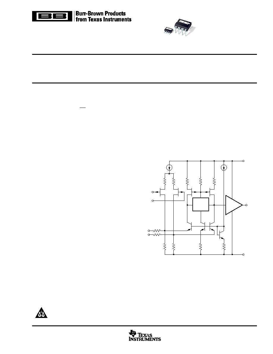
DESCRIPTION
The OPA604 is a FET-input operational amplifier designed
for enhanced AC performance. Very low distortion, low noise
and wide bandwidth provide superior performance in high
quality audio and other applications requiring excellent dy-
namic performance.
New circuit techniques and special laser trimming of dynamic
circuit performance yield very low harmonic distortion. The
result is an op amp with exceptional sound quality. The low-
noise FET input of the OPA604 provides wide dynamic
range, even with high source impedance. Offset voltage is
laser-trimmed to minimize the need for interstage coupling
capacitors.
The OPA604 is available in 8-pin plastic mini-DIP and SO-8
surface-mount packages, specified for the ≠25
∞
C to +85
∞
C
temperature range.
Distortion
Rejection
Circuitry
(1)
(3)
(+)
(2)
(≠)
(7)
V+
(6)
V
O
(4)
V≠
Output
Stage
(1)
NOTE: (1) Patents Granted: #5053718, 5019789
(5)
(1)
OPA6
04
OPA6
04
SBOS019A ≠ JANUARY 1992 ≠ SEPTEMBER 2003
www.ti.com
PRODUCTION DATA information is current as of publication date.
Products conform to specifications per the terms of Texas Instruments
standard warranty. Production processing does not necessarily include
testing of all parameters.
Copyright © 1992-2003, Texas Instruments Incorporated
Please be aware that an important notice concerning availability, standard warranty, and use in critical applications of
Texas Instruments semiconductor products and disclaimers thereto appears at the end of this data sheet.
All trademarks are the property of their respective owners.
OPA604
2
SBOS019A
www.ti.com
ABSOLUTE MAXIMUM RATINGS
Power Supply Voltage .......................................................................
±
25V
Input Voltage ............................................................... (V≠)≠1V to (V+)+1V
Output Short Circuit to Ground ................................................ Continuous
Operating Temperature .................................................. ≠40
∞
C to +100
∞
C
Storage Temperature ...................................................... ≠40
∞
C to +125
∞
C
Junction Temperature .................................................................... +150
∞
C
Lead Temperature (soldering, 10s) AP .......................................... +300
∞
C
Lead Temperature (soldering, 3s) AU ............................................ +260
∞
C
PIN CONFIGURATION
Top View
DIP, SOIC
1
2
3
4
Offset Trim
≠In
+In
≠V
S
8
7
6
5
No Internal Connection
+V
S
Output
Offset Trim
ELECTROSTATIC
DISCHARGE SENSITIVITY
Any integrated circuit can be damaged by ESD. Texas Instru-
ments recommends that all integrated circuits be handled with
appropriate precautions. Failure to observe proper handling
and installation procedures can cause damage.
ESD damage can range from subtle performance degradation
to complete device failure. Precision integrated circuits may be
more susceptible to damage because very small parametric
changes could cause the device not to meet published speci-
fications.
PACKAGE/ORDERING INFORMATION
For the most current package and ordering information, see
to the Package Option Addendum at the end of this data
sheet.
OPA604
3
SBOS019A
www.ti.com
ELECTRICAL CHARACTERISTICS
T
A
= +25
∞
C, V
S
=
±
15V, unless otherwise noted.
OPA604AP, AU
PARAMETER
CONDITION
MIN
TYP
MAX
UNITS
OFFSET VOLTAGE
Input Offset Voltage
±
1
±
5
mV
Average Drift
±
8
µ
V/
∞
C
Power Supply Rejection
V
S
=
±
5 to
±
24V
80
100
dB
INPUT BIAS CURRENT
(1)
Input Bias Current
V
CM
= 0V
50
pA
Input Offset Current
V
CM
= 0V
±
3
pA
NOISE
Input Voltage Noise
Noise Density: f = 10Hz
25
nV/
Hz
f = 100Hz
15
nV/
Hz
f = 1kHz
11
nV/
Hz
f = 10kHz
10
nV/
Hz
Voltage Noise, BW = 20Hz to 20kHz
1.5
µ
V
PP
Input Bias Current Noise
Current Noise Density, f = 0.1Hz to 20kHz
4
fA/
Hz
INPUT VOLTAGE RANGE
Common-Mode Input Range
±
12
±
13
V
Common-Mode Rejection
V
CM
=
±
12V
80
100
dB
INPUT IMPEDANCE
Differential
10
12
|| 8
|| pF
Common-Mode
10
12
|| 10
|| pF
OPEN-LOOP GAIN
Open-Loop Voltage Gain
V
O
=
±
10V, R
L
= 1k
80
100
dB
FREQUENCY RESPONSE
Gain-Bandwidth Product
G = 100
20
MHz
Slew Rate
20V
PP
, R
L
= 1k
15
25
V/
µ
s
Settling Time: 0.01%
G = ≠1, 10V Step
1.5
µ
s
0.1%
1
µ
s
Total Harmonic Distortion + Noise (THD+N)
G = 1, f = 1kHz
0.0003
%
V
O
= 3.5Vrms, R
L
= 1k
OUTPUT
Voltage Output
R
L
= 600
±
11
±
12
V
Current Output
V
O
=
±
12V
±
35
mA
Short Circuit Current
±
40
mA
Output Resistance, Open-Loop
25
POWER SUPPLY
Specified Operating Voltage
±
15
V
Operating Voltage Range
±
4.5
±
24
V
Current
±
5.3
±
7
mA
TEMPERATURE RANGE
Specification
≠25
+85
∞
C
Storage
≠40
+125
∞
C
Thermal Resistance
(2)
,
JA
90
∞
C/W
NOTES: (1) Typical performance, measured fully warmed-up. (2) Soldered to circuit board--see text.

OPA604
4
SBOS019A
www.ti.com
TYPICAL CHARACTERISTICS
T
A
= +25
∞
C, V
S
=
±
15V, unless otherwise noted.
TOTAL HARMONIC DISTORTION + NOISE
vs FREQUENCY
Frequency (Hz)
THD + N (%)
1
0.1
0.01
0.001
0.0001
20
100
1k
10k
20k
G = 100V/V
G = 10V/V
G = 1V/V
Measurement BW = 80kHz
See "Distortion Measure-
ments" for description of
test method.
1k
V =
3.5Vrms
O
TOTAL HARMONIC DISTORTION + NOISE
vs OUTPUT VOLTAGE
Output Voltage (V
PP
)
THD + N (%)
0.1
1
10
100
0.1
0.01
0.001
0.0001
1k
V
O
f = 1kHz
Measurement BW = 80kHz
See "Distortion Measurements"
for description of test method.
OPEN-LOOP GAIN/PHASE vs FREQUENCY
Frequency (Hz)
Voltage Gain (dB)
120
100
80
60
40
20
0
≠20
1
10
100
1k
10k
100k
1M
10M
0
≠45
≠90
≠135
≠180
Phase Shift (Degrees)
G
INPUT VOLTAGE AND CURRENT NOISE
SPECTRAL DENSITY vs FREQUENCY
Frequency (Hz)
Voltage Noise (nV/ Hz)
1
1k
100
10
1
10
100
1k
10k
100k
1M
Current Noise (fA/ Hz)
1k
100
10
1
Voltage Noise
Current Noise
INPUT BIAS AND INPUT OFFSET CURRENT
vs TEMPERATURE
Ambient Temperature (∞C)
Input Bias Current (pA)
≠75
100nA
10nA
1nA
100
10
1
Input Offset Current (pA)
10nA
1nA
100
10
1
0.1
≠50
≠25
0
25
50
75
100
125
Input
Offset Current
Input
Bias Current
INPUT BIAS AND INPUT OFFSET CURRENT
vs INPUT COMMON-MODE VOLTAGE
Common-Mode Voltage (V)
Input Bias Current (pA)
≠15
10nA
1nA
100
10
Input Offset Current (pA)
1nA
100
10
1
≠10
≠5
0
5
10
15
Input
Offset Current
Input
Bias Current

OPA604
5
SBOS019A
www.ti.com
TYPICAL CHARACTERISTICS
(Cont.)
T
A
= +25
∞
C, V
S
=
±
15V, unless otherwise noted.
COMMON-MODE REJECTION
vs COMMON-MODE VOLTAGE
Common-Mode Voltage (V)
Common-Mode Rejection (dB)
≠15
120
110
100
90
80
≠10
≠5
0
5
10
15
POWER SUPPLY AND COMMON-MODE
REJECTION vs FREQUENCY
Frequency (Hz)
Power Supply Rejection (dB)
10
120
100
80
60
40
20
0
100
1k
10k
100k
1M
10M
Common-Mode Rejection (dB)
120
100
80
60
40
20
0
+PSR
≠PSR
CMR
A
OL
, PSR, AND CMR vs SUPPLY VOLTAGE
Supply Voltage (±V
S
)
A
OL
, PSR, CMR (dB)
5
120
110
100
90
80
70
10
15
20
25
CMR
A
OL
PSR
GAIN-BANDWIDTH AND SLEW RATE
vs TEMPERATURE
Temperature (∞C)
Gain-Bandwidth (MHz)
≠75
28
24
20
16
12
≠25
25
75
125
Slew Rate (V/µs)
30
25
20
15
10
≠50
0
50
100
Slew Rate
Gain-Bandwidth
G = +100
INPUT BIAS CURRENT
vs TIME FROM POWER TURN-ON
Time After Power Turn-On (min)
Input Bias Current (pA)
0
1nA
100
10
1
1
2
3
4
5
V
S
=
±
24V
V
S
=
±
15V
V
S
=
±
5V
GAIN-BANDWIDTH AND SLEW RATE
vs SUPPLY VOLTAGE
Supply Voltage (±V
S
)
Gain-Bandwidth (MHz)
5
28
24
20
16
12
10
15
20
25
Slew Rate
Gain-Bandwidth
G = +100
Slew Rate (V/µs)
33
29
25
21
17

OPA604
6
SBOS019A
www.ti.com
TYPICAL CHARACTERISTICS
(Cont.)
T
A
= +25
∞
C, V
S
=
±
15V, unless otherwise noted.
0
SETTLING TIME vs CLOSED-LOOP GAIN
Closed-Loop Gain (V/V)
Settling Time (µs)
≠1
5
4
3
2
1
0
≠10
≠100
≠1000
0.01%
0.1%
V
O
= 10V Step
R
L
= 1k
C
L
= 50pF
MAXIMUM OUTPUT VOLTAGE SWING vs FREQUENCY
Frequency (Hz)
Output Voltage (Vp-p)
10k
30
20
10
0
100k
1M
10M
V = ±15V
S
SUPPLY CURRENT vs TEMPERATURE
Ambient Temperature (
∞
C)
Supply Current (mA)
-
75
7
6
5
4
3
-
50
-
25
0
25
50
75
100
125
V
S
=
±
24V
V
S
=
±
15V
V
S
=
±
5V
SHORT-CIRCUIT CURRENT vs TEMPERATURE
Ambient Temperature (∞C)
Short-Circuit Current (mA)
≠75
60
50
40
30
20
≠50
≠25
0
25
50
75
100
125
I
SC+
and I
SC≠
≠100
+100
2
1
Output Voltage (V)
SMALL-SIGNAL TRANSIENT RESPONSE
0
≠10
+10
10
5
Output Voltage (V)
LARGE-SIGNAL TRANSIENT RESPONSE

OPA604
7
SBOS019A
www.ti.com
TYPICAL CHARACTERISTICS
(Cont.)
T
A
= +25
∞
C, V
S
=
±
15V, unless otherwise noted.
APPLICATIONS INFORMATION
OFFSET VOLTAGE ADJUSTMENT
The OPA604 offset voltage is laser-trimmed and will require
no further trim for most applications. As with most amplifiers,
externally trimming the remaining offset can change drift
performance by about 0.3
µ
V/
∞
C for each 100
µ
V of adjusted
offset. The OPA604 can replace many other amplifiers by
leaving the external null circuit unconnected.
The OPA604 is unity-gain stable, making it easy to use in a
wide range of circuitry. Applications with noisy or high imped-
ance power supply lines may require decoupling capacitors
close to the device pins. In most cases, a 1
µ
F tantalum
capacitor at each power supply pin is adequate.
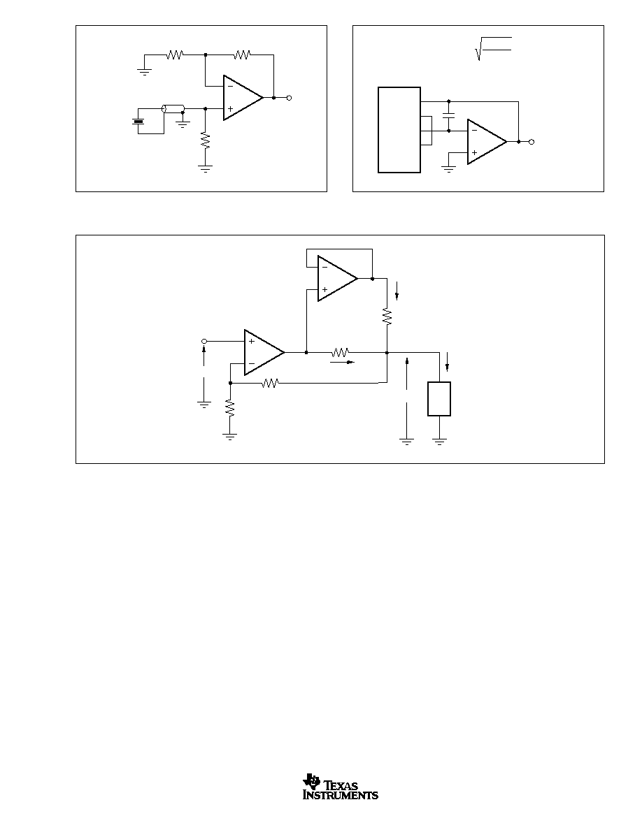
DISTORTION MEASUREMENTS
The distortion produced by the OPA604 is below the mea-
surement limit of virtually all commercially available equip-
ment. A special test circuit, however, can be used to extend
the measurement capabilities.
Op amp distortion can be considered an internal error source
which can be referred to the input. Figure 2 shows a circuit
which causes the op amp distortion to be 101 times greater
than normally produced by the op amp. The addition of R
3
to
the otherwise standard noninverting amplifier configuration
alters the feedback factor or noise gain of the circuit. The
closed-loop gain is unchanged, but the feedback available
for error correction is reduced by a factor of 101. This
extends the measurement limit, including the effects of the
signal-source purity, by a factor of 101. Note that the input
signal and load applied to the op amp are the same as with
conventional feedback without R
3
.
Validity of this technique can be verified by duplicating
measurements at high gain and/or high frequency where the
distortion is within the measurement capability of the test
equipment. Measurements for this data sheet were made
with the Audio Precision System One, which greatly simpli-
fies such repetitive measurements. The measurement tech-
nique can, however, be performed with manual distortion
measurement instruments.
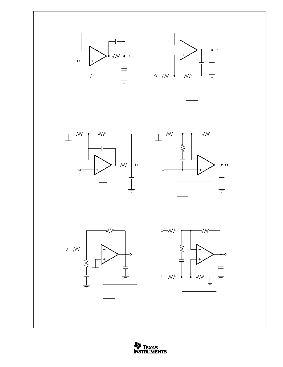
CAPACITIVE LOADS
The dynamic characteristics of the OPA604 have been
optimized for commonly encountered gains, loads and oper-
ating conditions. The combination of low closed-loop gain
and capacitive load will decrease the phase margin and may
lead to gain peaking or oscillations. Load capacitance reacts
with the op amp's open-loop output resistance to form an
additional pole in the feedback loop. Figure 3 shows various
circuits which preserve phase margin with capacitive load.
For details of analysis techniques and applications circuits,
refer to application bulletin AB-028 (SBOA015) located at
www.ti.com.
FIGURE 1. Offset Voltage Trim.
Supply Voltage, ±V
S
(V)
6
8
10
12
14
16
18
20
22
24
0.5
0.45
0.40
0.35
0.30
0.25
0.20
0.15
0.10
0.05
Power Dissipation (W)
POWER DISSIPATION vs SUPPLY VOLTAGE
No signal
or no load
Typical high-level
music R
L
= 600
Worst case sine
wave R
L
= 600
Ambient Temperature (∞C)
0
1.4
1.2
1.0
0.8
0.6
0.4
0.2
0
Total Power Dissipation (W)
MAXIMUM POWER DISSIPATION vs TEMPERATURE
25
50
75
100
125
150
J-A
= 90∞C/W
Soldered to
Circuit Board
(see text)
Maximum
Specified Operating
Temperature
85∞C
OPA604
±
50mV Typical
Trim Range
NOTE: (1) 50k
to 1M
Trim Potentiometer
(100k
Recommended)
+V
CC
≠V
CC
7
6
5
1
(1)
4
3
2

OPA604
8
SBOS019A
www.ti.com
For the unity-gain buffer, Figure 3a, stability is preserved by
adding a phase-lead network, R
C
and C
C
. Voltage drop
across R
C
will reduce output voltage swing with heavy loads.
An alternate circuit, Figure 3b, does not limit the output with
low load impedance. It provides a small amount of positive
feedback to reduce the net feedback factor. Input impedance
of this circuit falls at high frequency as op amp gain rolloff
reduces the bootstrap action on the compensation network.
Figures 3c and 3d show compensation techniques for
noninverting amplifiers. Like the follower circuits, the circuit in
Figure 3d eliminates voltage drop due to load current, but at
the penalty of somewhat reduced input impedance at high
frequency.
Figures 3e and 3f show input lead compensation networks
for inverting and difference amplifier configurations.
NOISE PERFORMANCE
Op amp noise is described by two parameters--noise volt-
age and noise current. The voltage noise determines the
noise performance with low source impedance. Low noise
bipolar-input op amps such as the OPA27 and OPA37
provide very low voltage noise. But if source impedance is
greater than a few thousand ohms, the current noise of
bipolar-input op amps react with the source impedance and
will dominate. At a few thousand ohms source impedance
and above, the OPA604 will generally provide lower noise.
POWER DISSIPATION
The OPA604 is capable of driving a 600
load with power-
supply voltages up to
±
24V. Internal power dissipation is
increased when operating at high power supply voltage. The
typical characteristic curve, Power Dissipation vs Power
Supply Voltage, shows quiescent dissipation (no signal or no
load) as well as dissipation with a worst case continuous sine
wave. Continuous high-level music signals typically produce
dissipation significantly less than worst-case sine waves.
Copper leadframe construction used in the OPA604 im-
proves heat dissipation compared to conventional plastic
packages. To achieve best heat dissipation, solder the de-
vice directly to the circuit board and use wide circuit board
traces.
OUTPUT CURRENT LIMIT
Output current is limited by internal circuitry to approximately
±
40mA at 25
∞
C. The limit current decreases with increasing
temperature as shown in the typical curves.
FIGURE 2. Distortion Test Circuit.
R
2
OPA604
R
1
R
3
V
O
= 10Vp-p
(3.5Vrms)
Generator
Output
Analyzer
Input
Audio Precision
System One
Analyzer
(1)
R
L
1k
IBM PC
or
Compatible
SIG.
GAIN
DIST.
GAIN
R
1
R
2
R
3
500
50
5k
5k
5k
50
500
1
10
100
101
101
101
NOTE: (1) Measurement BW = 80kHz
OPA604
9
SBOS019A
www.ti.com
FIGURE 3. Driving Large Capacitive Loads.
NOTE: Design equations and component values are approximate. User adjustment is required for optimum performance.
C
C
820pF
R
C
750
C
L
5000pF
e
i
C
C
=
120 X 10
≠12
C
L
(a)
e
o
C
L
5000pF
e
i
R
C
=
(b)
R
C
10
C
C
0.47µF
R
2
2k
R
2
4C
L
X 10
10
≠ 1
C
C
=
C
L
X 10
3
R
C
e
o
C
L
5000pF
R
2
10k
R
1
10k
C
C
=
50
R
2
C
L
e
i
R
C
25
C
C
24pF
(c)
e
o
C
L
5000pF
R
2
2k
R
1
2k
e
i
R
C
20
C
C
0.22µF
(d)
R
C
=
R
2
2C
L
X 10
10
≠ (1 + R
2
/R
1
)
e
o
C
L
5000pF
R
2
2k
R
1
2k
e
i
R
C
20
C
C
0.22µF
(e)
R
C
=
R
2
2C
L
X 10
10
≠ (1 + R
2
/R
1
)
e
o
C
L
5000pF
R
2
2k
R
1
2k
e
1
R
C
20
C
C
0.22µF
(f)
R
C
=
R
2
2C
L
X 10
10
≠ (1 + R
2
/R
1
)
R
3
2k
e
2
R
4
2k
e
o
OPA604
C
C
=
C
L
X 10
3
R
C
C
C
=
C
L
X 10
3
R
C
C
C
=
C
L
X 10
3
R
C
OPA604
OPA604
OPA604
OPA604
OPA604

OPA604
10
SBOS019A
www.ti.com
FIGURE 5. Three-Pole Generalized Immittance Converter (GIC) Low-Pass Filter.
FIGURE 4. Three-Pole Low-Pass Filter.
R
5
2k
V
O
C
3
1000pF
Low-pass
3-pole Butterworth
f
≠3dB
= 40kHz
R
1
6.04k
V
IN
R
2
4.02k
R
2
4.02k
C
2
1000pF
C
1
1000pF
R
4
5.36k
See Application Bulletin AB-026
for information on GIC filters.
1
2
OPA2604
1
2
OPA2604
OPA604
FIGURE 6. Differential Amplifier with Low-Pass Filter.
R
4
22k
R
3
10k
V
O
C
2
2000pF
R
2
22k
C
1
3000pF
R
1
2.7k
V
IN
f
p
= 20kHz
C
3
100pF
OPA604
V
O
G = 1
100pF
≠
V
IN
+
7.87k
7.87k
10k
10k
10k
10k
100kHz Input Filter
OPA604
1
2
OPA2604
1
2
OPA2604
OPA604
11
SBOS019A
www.ti.com
FIGURE 8. Digital Audio DAC I-V Amplifier.
FIGURE 7. High Impedance Amplifier.
FIGURE 9. Using Two OPA604 Op Amps to Double the Output Current to a Load.
OPA604
OPA604
A
1
A
2
V
IN
R
1
R
2
I
1
R
4
51
I
2
OPA604
R
3
51
I
L
= I
1
+ I
2
Load
V
OUT
= V
IN
(1+R
2
/R
1
)
V
OUT
OPA604
G = 101
(40dB)
100
10k
Piezoelectric
Transducer
1M
(1)
NOTE: (1) Provides input
bias current return path.
OPA604
V
O
= ±3Vp
R
F
= Internal feedback resistance = 1.5k
f
C
= Crossover frequency = 8MHz
C
1
(1)
NOTE: (1) C
1
C
OUT
2
R
f
f
c
To low-pass
filter.
OPA604
5
6
9
PCM63
20-bit
D/A
Converter
10

OPA604
12
SBOS019A
www.ti.com
1
0
0
1
I
C
(mA)
0
5
log
(V
O
)
1
2
3
4
f
O
2f
O
3f
O
4f
O
5f
O
V
BE
= 1kHz + DC Bias
V
BE
(V)
0.65
FFT
Frequency (kHz)
1
0
1
0
≠I
D
(mA)
0
5
log
(V
O
)
1
2
3
4
f
O
2f
O
3f
O
4f
O
5f
O
V
GS
= 1kHz + DC Bias
V
GS
(V)
FFT
Frequency (kHz)
V
O
I
D
V
GS
V
O
I
C
V
BE
FIGURE 10. I-V and Spectral Response of NPN and
JFET.
THE OPA604 DESIGN
The OPA604 uses FETs throughout the signal path,
including the input stage, input-stage load, and the
important phase-splitting section of the output stage.
Bipolar transistors are used where their attributes,
such as current capability are important, and where
their transfer characteristics have minimal impact.
The topology consists of a single folded-cascode gain
stage followed by a unity-gain output stage. Differen-
tial input transistors J
1
and J
2
are special large-geom-
etry, P-channel JFETs. Input stage current is a rela-
tively high 800
µ
A, providing high transconductance
and reducing voltage noise. Laser trimming of stage
currents and careful attention to symmetry yields a
nearly symmetrical slew rate of
±
25V/
µ
s.
The JFET input stage holds input bias current to
approximately 50pA or roughly 3000 times lower than
common bipolar-input audio op amps. This dramati-
cally reduces noise with high-impedance circuitry.
The drains of J
1
and J
2
are cascoded by Q
1
and Q
2
,
driving the input stage loads, FETs J
3
and J
4
. Distor-
tion reduction circuitry (patented) linearizes the open-
loop response and increases voltage gain. The 20MHz
bandwidth of the OPA604 further reduces distortion
through the user-connected feedback loop.
The output stage consists of a JFET phase-splitter
loaded into high speed all-NPN output drivers. Output
transistors are biased by a special circuit to prevent
cutoff, even with full output swing into 600
loads.
The following discussion is provided, recognizing that
not all measured performance behavior explains or
correlates with listening tests by audio experts. The
design of the OPA604 included consideration of both
objective performance measurements, as well as an
awareness of widely held theory on the success and
failure of previous op amp designs.
SOUND QUALITY
The sound quality of an op amp is often the crucial
selection criteria--even when a data sheet claims
exceptional distortion performance. By its nature, sound
quality is subjective. Furthermore, results of listening
tests can vary depending on application and circuit
configuration. Even experienced listeners in controlled
tests often reach different conclusions.
Many audio experts believe that the sound quality of a
high performance FET op amp is superior to that of
bipolar op amps. A possible reason for this is that
bipolar designs generate greater odd-order harmonics
than FETs. To the human ear, odd-order harmonics
have long been identified as sounding more unpleas-
ant than even-order harmonics. FETs, like vacuum
tubes, have a square-law I-V transfer function which is
more linear than the exponential transfer function of a
bipolar transistor. As a direct result of this square-law
characteristic, FETs produce predominantly even-or-
der harmonics. Figure 10 shows the transfer function of
a bipolar transistor and FET. Fourier transformation of
both transfer functions reveals the lower odd-order
harmonics of the FET amplifier stage.
SOUND QUALITY
Distortion
Rejection
Circuitry
(+)
(≠)
Output
Stage
R
3
1k
R
4
1k
R
8
3k
R
9
3k
R
1
75
R
2
75
R
5
500
R
7
4k
R
6
500
I
1
800µA
J
1
J
2
J
3
J
4
Q
4
Q
2
Q
3
Q
1
J
5
I
2
200µA
R
10
10k
R
11
10k

PACKAGING INFORMATION
ORDERABLE DEVICE
STATUS(1)
PACKAGE TYPE
PACKAGE DRAWING
PINS
PACKAGE QTY
OPA604AP
ACTIVE
PDIP
P
8
50
OPA604AU
ACTIVE
SOIC
D
8
100
OPA604AU/2K5
ACTIVE
SOIC
D
8
2500
(1) The marketing status values are defined as follows:
ACTIVE: Product device recommended for new designs.
LIFEBUY: TI has announced that the device will be discontinued, and a lifetime-buy period is in effect.
NRND: Not recommended for new designs. Device is in production to support existing customers, but TI does not recommend using this part in
a new design.
PREVIEW: Device has been announced but is not in production. Samples may or may not be available.
OBSOLETE: TI has discontinued the production of the device.
PACKAGE OPTION ADDENDUM
www.ti.com
3-Oct-2003
MECHANICAL DATA
MPDI001A ≠ JANUARY 1995 ≠ REVISED JUNE 1999
1
POST OFFICE BOX 655303
∑
DALLAS, TEXAS 75265
P (R-PDIP-T8)
PLASTIC DUAL-IN-LINE
8
4
0.015 (0,38)
Gage Plane
0.325 (8,26)
0.300 (7,62)
0.010 (0,25) NOM
MAX
0.430 (10,92)
4040082/D 05/98
0.200 (5,08) MAX
0.125 (3,18) MIN
5
0.355 (9,02)
0.020 (0,51) MIN
0.070 (1,78) MAX
0.240 (6,10)
0.260 (6,60)
0.400 (10,60)
1
0.015 (0,38)
0.021 (0,53)
Seating Plane
M
0.010 (0,25)
0.100 (2,54)
NOTES: A. All linear dimensions are in inches (millimeters).
B. This drawing is subject to change without notice.
C. Falls within JEDEC MS-001
For the latest package information, go to http://www.ti.com/sc/docs/package/pkg_info.htm
MECHANICAL DATA
MSOI002B ≠ JANUARY 1995 ≠ REVISED SEPTEMBER 2001
1
POST OFFICE BOX 655303
∑
DALLAS, TEXAS 75265
D (R-PDSO-G**)
PLASTIC SMALL-OUTLINE PACKAGE
8 PINS SHOWN
8
0.197
(5,00)
A MAX
A MIN
(4,80)
0.189
0.337
(8,55)
(8,75)
0.344
14
0.386
(9,80)
(10,00)
0.394
16
DIM
PINS **
4040047/E 09/01
0.069 (1,75) MAX
Seating Plane
0.004 (0,10)
0.010 (0,25)
0.010 (0,25)
0.016 (0,40)
0.044 (1,12)
0.244 (6,20)
0.228 (5,80)
0.020 (0,51)
0.014 (0,35)
1
4
8
5
0.150 (3,81)
0.157 (4,00)
0.008 (0,20) NOM
0
∞
≠ 8
∞
Gage Plane
A
0.004 (0,10)
0.010 (0,25)
0.050 (1,27)
NOTES: A. All linear dimensions are in inches (millimeters).
B. This drawing is subject to change without notice.
C. Body dimensions do not include mold flash or protrusion, not to exceed 0.006 (0,15).
D. Falls within JEDEC MS-012

IMPORTANT NOTICE
Texas Instruments Incorporated and its subsidiaries (TI) reserve the right to make corrections, modifications,
enhancements, improvements, and other changes to its products and services at any time and to discontinue
any product or service without notice. Customers should obtain the latest relevant information before placing
orders and should verify that such information is current and complete. All products are sold subject to TI's terms
and conditions of sale supplied at the time of order acknowledgment.
TI warrants performance of its hardware products to the specifications applicable at the time of sale in
accordance with TI's standard warranty. Testing and other quality control techniques are used to the extent TI
deems necessary to support this warranty. Except where mandated by government requirements, testing of all
parameters of each product is not necessarily performed.
TI assumes no liability for applications assistance or customer product design. Customers are responsible for
their products and applications using TI components. To minimize the risks associated with customer products
and applications, customers should provide adequate design and operating safeguards.
TI does not warrant or represent that any license, either express or implied, is granted under any TI patent right,
copyright, mask work right, or other TI intellectual property right relating to any combination, machine, or process
in which TI products or services are used. Information published by TI regarding third-party products or services
does not constitute a license from TI to use such products or services or a warranty or endorsement thereof.
Use of such information may require a license from a third party under the patents or other intellectual property
of the third party, or a license from TI under the patents or other intellectual property of TI.
Reproduction of information in TI data books or data sheets is permissible only if reproduction is without
alteration and is accompanied by all associated warranties, conditions, limitations, and notices. Reproduction
of this information with alteration is an unfair and deceptive business practice. TI is not responsible or liable for
such altered documentation.
Resale of TI products or services with statements different from or beyond the parameters stated by TI for that
product or service voids all express and any implied warranties for the associated TI product or service and
is an unfair and deceptive business practice. TI is not responsible or liable for any such statements.
Following are URLs where you can obtain information on other Texas Instruments products and application
solutions:
Products
Applications
Amplifiers
amplifier.ti.com
Audio
www.ti.com/audio
Data Converters
dataconverter.ti.com
Automotive
www.ti.com/automotive
DSP
dsp.ti.com
Broadband
www.ti.com/broadband
Interface
interface.ti.com
Digital Control
www.ti.com/digitalcontrol
Logic
logic.ti.com
Military
www.ti.com/military
Power Mgmt
power.ti.com
Optical Networking
www.ti.com/opticalnetwork
Microcontrollers
microcontroller.ti.com
Security
www.ti.com/security
Telephony
www.ti.com/telephony
Video & Imaging
www.ti.com/video
Wireless
www.ti.com/wireless
Mailing Address:
Texas Instruments
Post Office Box 655303 Dallas, Texas 75265
Copyright
2003, Texas Instruments Incorporated