 | ÐлекÑÑоннÑй компоненÑ: PCM1725 | СкаÑаÑÑ:  PDF PDF  ZIP ZIP |
SoundPlus Stereo Audio Digital-To-Analog Converter 16 Bits, 96kHz Sampling
®
1
PCM1725
Stereo Audio
DIGITAL-TO-ANALOG CONVERTER
16 Bits, 96kHz Sampling
TM
PCM1725
DESCRIPTION
The PCM1725 is a complete low cost stereo audio
digital-to-analog converter (DAC), operating off of a
256f
S
or 384f
S
system clock. The DAC contains a 3rd-
order
modulator, a digital interpolation filter, and
an analog output amplifier. The PCM1725 accepts
16-bit input data in either normal or I
2
S formats.
The digital filter performs an 8X interpolation function
and includes de-emphasis at 44.1kHz. The PCM1725
can accept digital audio sampling frequencies from
16kHz to 96kHz, always at 8X oversampling.
The PCM1725 is ideal for low-cost, CD-quality con-
sumer audio applications.
®
FEATURES
q
COMPLETE STEREO DAC: Includes Digital
Filter and Output Amp
q
DYNAMIC RANGE: 95dB
q
MULTIPLE SAMPLING FREQUENCIES:
16kHz to 96kHz
q
8X OVERSAMPLING DIGITAL FILTER
q
SYSTEM CLOCK: 256f
S
/ 384f
S
q
NORMAL OR I
2
S DATA INPUT FORMATS
q
SMALL 14-PIN SOIC PACKAGE
PCM1725
International Airport Industrial Park · Mailing Address: PO Box 11400, Tucson, AZ 85734 · Street Address: 6730 S. Tucson Blvd., Tucson, AZ 85706 · Tel: (520) 746-1111 · Twx: 910-952-1111
Internet: http://www.burr-brown.com/ · FAXLine: (800) 548-6133 (US/Canada Only) · Cable: BBRCORP · Telex: 066-6491 · FAX: (520) 889-1510 · Immediate Product Info: (800) 548-6132
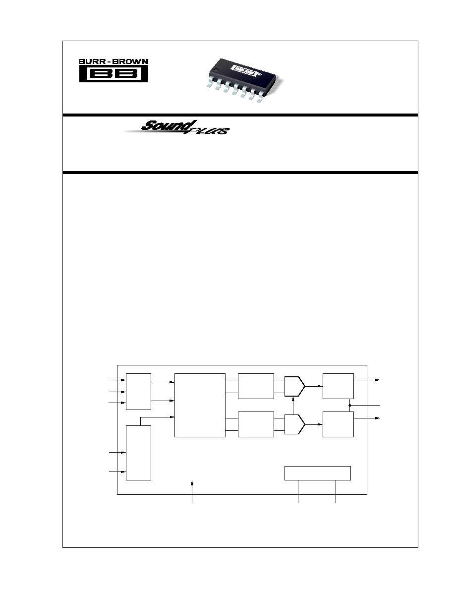
Serial
Input
I/F
Mode
Control
I/F
8X Oversampling
Digital Filter
SCKI
256f
S
/384f
S
V
CC
GND
Multi-level
Delta-Sigma
Modulator
V
OUT
L
CAP
DAC
Multi-level
Delta-Sigma
Modulator
Low-pass
Filter
Low-pass
Filter
V
OUT
R
DAC
FORMAT
LRCIN
DIN
BCKIN
DM
Power Supply
© 1997 Burr-Brown Corporation
PDS-1373C
Printed in U.S.A. January, 1998
SBAS067
®
2
PCM1725
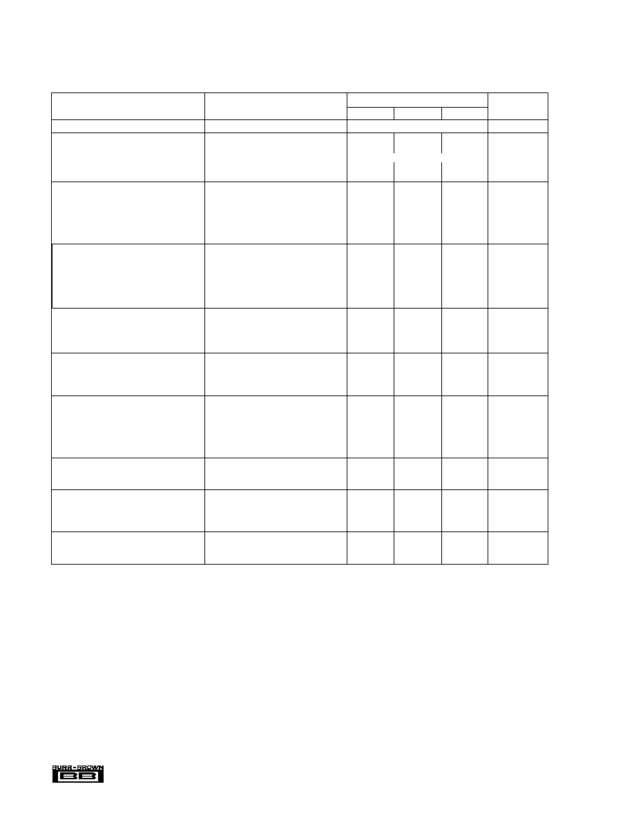
SPECIFICATIONS
All specifications at +25
°
C, +V
CC
= +5V, f
S
= 44.1kHz, and 16-bit input data, SYSCLK = 384f
S
, unless otherwise noted.
The information provided herein is believed to be reliable; however, BURR-BROWN assumes no responsibility for inaccuracies or omissions. BURR-BROWN assumes
no responsibility for the use of this information, and all use of such information shall be entirely at the user's own risk. Prices and specifications are subject to change
without notice. No patent rights or licenses to any of the circuits described herein are implied or granted to any third party. BURR-BROWN does not authorize or warrant
any BURR-BROWN product for use in life support devices and/or systems.
PCM1725
PARAMETER
CONDITIONS
MIN
TYP
MAX
UNITS
RESOLUTION
16
Bits
DATA FORMAT
Audio Data Interface Format
Standard /I
2
S
Audio Data Format
Binary Two's Complement
Sampling Frequency (f
S
)
16
96
kHz
Internal System Clock Frequency
256f
S
/384f
S
DIGITAL INPUT/OUTPUT
Logic Level
TTL
Input Logic Level
V
IH
(1)
2.0
VDC
V
IL
(1)
0.8
VDC
Input Logic Current: I
IN
(1)
±
0.8
µ
A
DYNAMIC PERFORMANCE
(2)
f = 991kHz
THD+N at FS (0dB)
83
78
dB
THD+N at 60dB
32
dB
Dynamic Range
A-weighted
90
95
dB
Signal-to-Noise Ratio
A-weighted
90
97
dB
Channel Separation
88
95
dB
DC ACCURACY
Gain Error
±
1.0
±
5.0
% of FSR
Gain Mismatch, Channel-to-Channel
±
1.0
±
5.0
% of FSR
Bipolar Zero Error
V
OUT
= V
CC
/2 at BPZ
±
20
±
50
mV
ANALOG OUTPUT
Output Voltage
Full Scale (0dB)
0.62 x V
CC
Vp-p
Center Voltage
V
CC
/2
VDC
Load Impedance
AC Load
10
k
DIGITAL FILTER PERFORMANCE
Passband
0.445
f
S
Stopband
0.555
f
S
Passband Ripple
±
0.17
dB
Stopband Attenuation
35
dB
Delay Time
11.125/f
S
sec
INTERNAL ANALOG FILTER
3dB Bandwidth
100
kHz
Passband Response
f = 20kHz
0.16
dB
POWER SUPPLY REQUIREMENTS
Voltage Range
4.5
5
5.5
VDC
Supply Current
13
18
mA
Power Dissipation
65
90
mW
TEMPERATURE RANGE
Operation
25
+85
°
C
Storage
55
+125
°
C
NOTES: (1) Pins 1, 2, 3, 12, 13: LRCIN, DIN, BCKIN, DM, FORMAT (Schmitt Trigger Input); Pin 14: SCKI. (2) Dynamic performance specs are tested with 20kHz
low pass filter and THD+N specs are tested with 30kHz LPF, 400Hz HPF, Average-Mode.
®
3
PCM1725
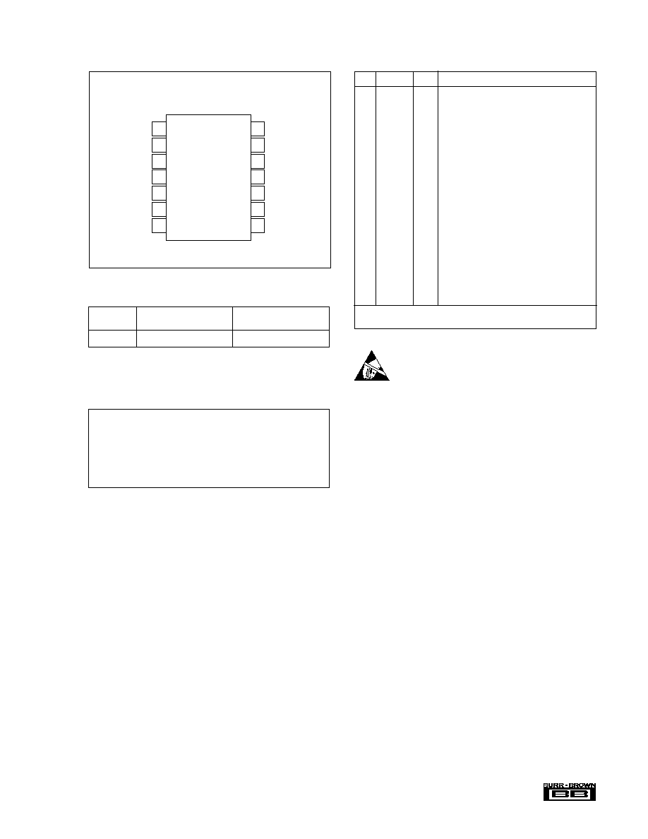
PIN ASSIGNMENTS
PIN
NAME
I/O
FUNCTION
1
(1)
LRCIN
IN
Sample Rate Clock Input
2
(1)
DIN
IN
Audio Data Input
3
(1)
BCKIN
IN
Bit Clock Input for Audio Data.
4
NC
--
No Connection
5
CAP
--
Common Pin of Analog Output Amp
6
V
OUT
R
OUT
Right-Channel Analog Output
7
GND
--
Ground
8
V
CC
--
Power Supply
9
V
OUT
L
OUT
Left-Channel Analog Output
10
NC
--
No Connection
11
NC
--
No Connection
12
(2)
DM
IN
De-emphasis Control
HIGH: De-emphasis ON
LOW: De-emphasis OFF
13
(2)
FORMAT
--
Audio Data Format Select
HIGH: I
2
S Data Format
LOW: Standard Data Format
14
SCKI
IN
System Clock Input (256f
S
or 384f
S
)
NOTES: (1) Schmitt Trigger input. (2) Schmitt Trigger input with internal
pull-up.
PIN CONFIGURATION
TOP VIEW
SOIC
LRCIN
DIN
BCKIN
NC
CAP
V
OUT
R
GND
SCKI
FORMAT
DM
NC
NC
V
OUT
L
V
CC
1
2
3
4
5
6
7
14
13
12
11
10
9
8
PCM1725
PACKAGE INFORMATION
PACKAGE DRAWING
PRODUCT
PACKAGE
NUMBER
(1)
PCM1725U
14 Pin SOIC
235
NOTE: (1) For detailed drawing and dimension table, please see end of data
sheet, or Appendix C of Burr-Brown IC Data Book.
ABSOLUTE MAXIMUM RATINGS
Power Supply Voltage ....................................................................... +6.5V
+V
CC
to +V
DD
Difference ...................................................................
±
0.1V
Input Logic Voltage .................................................. 0.3V to (V
DD
+ 0.3V)
Power Dissipation .......................................................................... 290mW
Operating Temperature Range ......................................... 25
°
C to +85
°
C
Storage Temperature ...................................................... 55
°
C to +125
°
C
Lead Temperature (soldering, 5s) .................................................. +260
°
C
Thermal Resistance,
JA
.............................................................. +90
°
C/W
ELECTROSTATIC
DISCHARGE SENSITIVITY
This integrated circuit can be damaged by ESD. Burr-Brown
recommends that all integrated circuits be handled with
appropriate precautions. Failure to observe proper handling
and installation procedures can cause damage.
ESD damage can range from subtle performance degradation
to complete device failure. Precision integrated circuits may
be more susceptible to damage because very small parametric
changes could cause the device not to meet its published
specifications.
®
4
PCM1725
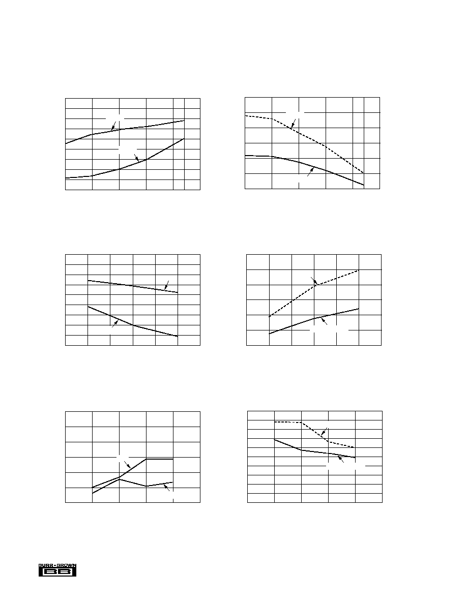
TYPICAL PERFORMANCE CURVES
At T
A
= +25
°
C, +V
CC
= +5V, f
S
= 44.1kHz, SYSCLK = 256f
S
, unless otherwise noted.
DYNAMIC PERFORMANCE
THD+N vs TEMPERATURE
Temperature (°C)
THD+N at 0dB (%)
0.009
0.008
0.007
0.006
0.005
0.004
0.003
0.002
0.001
0
25
0
25
50
75
85
100
THD+N at 60dB (%)
3.2
3.1
3.0
2.9
2.8
2.7
2.6
2.5
2.4
2.3
60dB
0dB
SNR, DYNAMIC RANGE vs TEMPERATURE
Temperature (°C)
SNR (dB)
99
98
97
96
95
94
93
99
98
97
96
95
94
93
25
0
25
50
75
85
100
Dynamic Range (dB)
Dynamic Range
SNR
THD+N vs POWER SUPPLY
V
CC
(V)
THD+N at 0dB (%)
0.009
0.008
0.007
0.006
0.005
0.004
0.003
0.002
0.001
0
4.5
4.75
5.0
5.25
5.5
THD+N at 60dB (%)
3.2
3.1
3.0
2.9
2.8
2.7
2.6
2.5
2.4
2.3
60dB
0dB
THD+N vs SAMPLING RATE
Sampling Rate (kHz)
THD+N at 0dB (%)
0.016
0.014
0.012
0.01
0.008
0.006
0.004
5.2
4.7
4.2
3.7
3.2
2.7
2.2
44.1
48
88.2
96
THD+N AT 60dB (%)
60dB
0dB
SNR, DYNAMIC RANGE vs SAMPLING RATE
Sampling Rate (kHz)
SNR (dB)
98
97
96
95
94
93
92
91
90
89
88
98
97
96
95
94
93
92
91
90
89
88
44.1
48
88.2
96
Dynamic Range (dB)
Dynamic Range
SNR
SNR, DYNAMIC RANGE vs POWER SUPPLY
V
CC
(V)
SNR (dB)
99
98
97
96
95
94
93
99
98
97
96
95
94
93
4.5
4.75
5.0
5.25
5.5
Dynamic Range (dB)
Dynamic Range
SNR
®
5
PCM1725
TYPICAL PERFORMANCE CURVES
At T
A
= +25
°
C, +V
CC
= +V
DD
= +5V, f
S
= 44.1kHz, and 16-bit input data, SYSCLK = 384f
S
, unless otherwise noted.
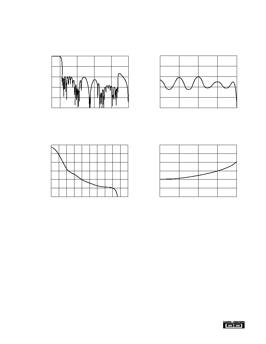
DIGITAL FILTER
0 0.4536f
S
1.3605f
S
2.2675f
S
3.1745f
S
4.0815f
S
0
20
40
60
80
100
dB
OVERALL FREQUENCY CHARACTERISTIC
Frequency (Hz)
PASSBAND RIPPLE CHARACTERISTIC
0
0.2
0.4
0.6
0.8
1
0
0.1134f
S
0.2268f
S
0.3402f
S
0.4535f
S
dB
Frequency (Hz)
DE-EMPHASIS FREQUENCY RESPONSE (44.1kHz)
Frequency (kHz)
Level (dB)
0
2
4
6
8
10
12
0
5
10
15
20
25
DE-EMPHASIS FREQUENCY ERROR (44.1kHz)
Frequency (kHz)
Error (dB)
0.6
0.4
0.2
0.0
0.2
0.4
0.6
0
4999.8375
9999.675
14999.5125
19999.35
®
6
PCM1725
FIGURE 1. "Normal" Data Input Timing.
FIGURE 2. "I
2
S" Data Input Timing.
LRCKIN
BCKIN
DIN
1.4V
1.4V
1.4V
t
BCH
t
BCL
t
LB
t
BL
t
DS
BCKIN Pulse Cycle Time
BCKIN Pulse Width High
BCKIN Pulse Width Low
BCKIN Rising Edge to LRCIN Edge
LRCIN Edge to BCKIN Rising Edge
DIN Set-up Time
DIN Hold Time
: t
BCY
: t
BCH
: t
BCL
: t
BL
: t
LB
: t
DS
: t
DH
: 100ns (min)
: 50ns (min)
: 50ns (min)
: 30ns (min)
: 30ns (min)
: 30ns (min)
: 30ns (min)
t
DH
t
BCY
FIGURE 3. Audio Data Input Timing.
SYSTEM CLOCK
The system clock for PCM1725 must be either 256f
S
or
384f
S
, where f
S
is the audio sampling frequency (LRCIN),
typically 32kHz, 44.1kHz or 48kHz. The system clock is
used to operate the digital filter and the noise shaper. The
system clock input (SCKI) is at pin 14. Timing conditions
for SCKI are shown in Figure 4.
System Clock Pulse Width High
t
SCKIH
13ns (min)
System Clock Pulse Width Low
t
SCKIL
13ns (min)
t
SCKIH
SCKI
t
SCKIL
2.0V
0.8V
FIGURE 4. System Clock Timing Requirements.
14
15
16
1
2
3
14
15
1/fs
L_ch
R_ch
MSB
LSB
16
LRCIN (pin 1)
BCKIN (pin 3)
AUDIO DATA WORD = 16-BIT
DIN (pin 2)
1
2
3
14
15
MSB
LSB
16
1
2
3
14
15
1/fs
L_ch
R_ch
MSB
LSB
16
LRCIN (pin 1)
BCKIN (pin 3)
AUDIO DATA WORD = 16-BIT
DIN (pin 2)
1
2
3
14
15
MSB
LSB
16
2
1
®
7
PCM1725
PCM1725 has a system clock detection circuit which auto-
matically detects the frequency, either 256f
S
or 384f
S
. The
system clock should be synchronized with LRCIN (pin 1),
but PCM1725 can compensate for phase differences. If the
phase difference between LRCIN and system clock is greater
than
±
6 bit clocks (BCKIN), the synchronization is per-
formed automatically. The analog outputs are forced to a
bipolar zero state (V
CC
/2) during the synchronization func-
tion. Table I shows the typical system clock frequency
inputs for the PCM1725.
SYSTEM CLOCK
FREQUENCY (MHz)
256f
S
384f
S
32kHz
8.192
12.288
44.1kHz
11.2896
16.9340
48kHz
12.288
18.432
SAMPLING
RATE (LRCIN)
TABLE I. System Clock Frequencies vs Sampling Rate.
TYPICAL CONNECTION DIAGRAM
Figure 5 illustrates the typical connection diagram for
PCM1725 used in a stand-alone application.
INPUT DATA FORMAT
PCM1725 can accept input data in either normal (MSB-first,
right-justified) or I
2
S formats. When pin 13 (FORMAT) is
LOW, normal data format is selected; a HIGH on pin 13
selects I
2
S format.
FORMAT
0
Normal Format (MSB-first, right-justified)
1
I
2
S Format (Philips serial data protocol)
TABLE II. Input Format Selection.
FIGURE 6. Internal Power-On Reset Timing.
DIN
BCKIN
LRCIN
2
3
1
13
12
FORMAT
DM
SCKI
9
5
7
8
6
14
PCM
Audio Data
Processor
256f
S
/384f
S
CLK
GND
Mode Control
Lch Analog Out
+5V Analog
Rch Analog Out
V
CC
V
OUT
L
V
OUT
R
CAP
PCM1725
+
10µF
Post
LPF
Post
LPF
FIGURE 5. Typical Connection Diagram.
RESET
PCM1725 has an internal power-on reset circuit. The internal
power-on reset initializes (resets) when the supply voltage
V
CC
> 2.2V (typ). The power-on reset has an initialization
period equal to 1024 system clock periods after V
CC
> 2.2V.
During the initialization period, the outputs of the DAC are
invalid, and the analog outputs are forced to V
CC
/2. Figure 6
illustrates the power-on reset and reset-pin reset timing.
DE-EMPHASIS CONTROL
Pin 12 (DM) enables PCM1725's de-emphasis function. De-
emphasis operates only at 44.1kHz.
DM
0
DEM OFF
1
DEM ON (44.1kHz)
TABLE III. De-Emphasis Control Selection.
1024 system (= SCKI) clocks
Reset
Reset Removal
2.6V
2.2V
1.8V
V
CC
Internal Reset
SCKI Clock
®
8
PCM1725
APPLICATION
CONSIDERATIONS
DELAY TIME
There is a finite delay time in delta-sigma converters. In A/D
converters, this is commonly referred to as latency. For a
delta-sigma D/A converter, delay time is determined by the
order number of the FIR filter stage, and the chosen sampling
rate. The following equation expresses the delay time of
PCM1725:
T
D
= 11.125 x 1/f
S
For f
S
= 44.1kHz, T
D
= 11.125/44.1kHz = 251.4
µ
s
Applications using data from a disc or tape source, such as
CD audio, CD-Interactive, Video CD, DAT, Minidisc,
etc., generally are not affected by delay time. For some
professional applications such as broadcast audio for stu-
dios, it is important for total delay time to be less than 2ms.
OUTPUT FILTERING
For testing purposes all dynamic tests are done on the
PCM1725 using a 20kHz low pass filter. This filter limits
the measured bandwidth for THD+N, etc. to 20kHz. Failure
to use such a filter will result in higher THD+N and lower
SNR and Dynamic Range readings than are found in the
specifications. The low pass filter removes out of band
noise. Although it is not audible, it may affect dynamic
specification numbers.
The performance of the internal low pass filter from DC to
24kHz is shown in Figure 7. The higher frequency rolloff of
the filter is shown in Figure 8. If the user's application has
the PCM1725 driving a wideband amplifier, it is recom-
mended to use an external low pass filter. A simple 3rd-
order filter is shown in Figure 9. For some applications, a
passive RC filter or 2nd-order filter may be adequate.
BYPASSING POWER SUPPLIES
The power supplies should be bypassed as close as possible
to the unit. It is also recommended to include a 0.1
µ
F ceramic
capacitor in parallel with the 10
µ
F tantalum bypass capacitor.
1.0
0.5
0
0.5
1.0
dB
20
Frequency (Hz)
100
1k
10k
24k
INTERNAL ANALOG FILTER FREQUENCY RESPONSE
(20Hz~24kHz, Expanded Scale)
FIGURE 7. Low Pass Filter Frequency Response.
10
5
0
5
10
15
20
25
30
35
40
45
50
55
10
100
1k
10k
100k
1M
10M
Frequency (Hz)
dB
60
INTERNAL ANALOG FILTER FREQUENCY RESPONSE
(10Hz~10MHz)
FIGURE 8. Low Pass Filter Wideband Frequency Response.
10k
10k
10k
1500pF
100pF
680pF
+
V
SIN
90
0
90
180
270
360
100
1k
10k
100k
1M
GAIN vs FREQUENCY
Frequency (Hz)
Phase (°)
6
14
34
54
74
94
Gain (dB)
Gain
Phase
OPA134
FIGURE 9. 3rd-Order LPF.
®
9
PCM1725
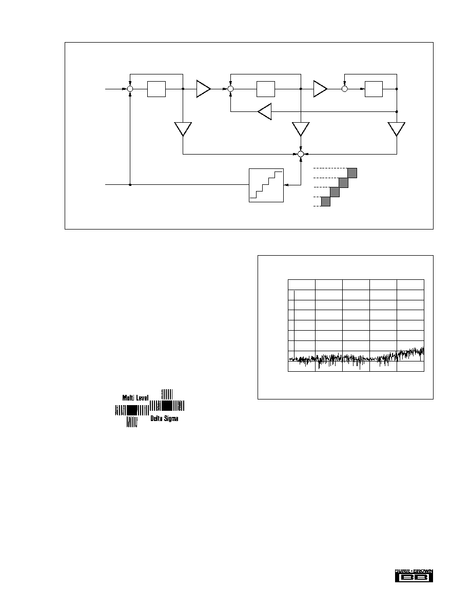
FIGURE 10. 5-Level
Modulator Block Diagram.
FIGURE 11. Quantization Noise Spectrum.
Out
48f
S
(384f
S
)
64f
S
(256f
S
)
In
8f
S
18-Bit
+
+
+
4
3
2
1
0
5-level Quantizer
+
+
Z
1
+
+
Z
1
+
+
Z
1
THEORY OF OPERATION
The delta-sigma section of PCM1725 is based on a 5-level
amplitude quantizer and a 3rd-order noise shaper. This
section converts the oversampled input data to 5-level delta-
sigma format. A block diagram of the 5-level delta-sigma
modulator is shown in Figure 10. This 5-level delta-sigma
modulator has the advantage of stability and clock jitter over
the typical one-bit (2-level) delta-sigma modulator.
The combined oversampling rate of the delta-sigma modu-
lator and the internal 8X interpolation filter is 96f
S
for a
384f
S
system clock, and 64f
S
for a 256f
S
system clock. The
theoretical quantization noise performance of the 5-level
delta-sigma modulator is shown in Figure 11.
5-LEVEL
MODULATOR
Frequency (kHz)
Gain (dB)
20
0
20
40
60
80
100
120
140
160
0
5
10
15
20
25
PACKAGING INFORMATION
ORDERABLE DEVICE
STATUS(1)
PACKAGE TYPE
PACKAGE DRAWING
PINS
PACKAGE QTY
PCM1725U
ACTIVE
SOIC
D
14
56
PCM1725U/2K
ACTIVE
SOIC
D
14
2000
(1) The marketing status values are defined as follows:
ACTIVE: Product device recommended for new designs.
LIFEBUY: TI has announced that the device will be discontinued, and a lifetime-buy period is in effect.
NRND: Not recommended for new designs. Device is in production to support existing customers, but TI does not recommend using this part in
a new design.
PREVIEW: Device has been announced but is not in production. Samples may or may not be available.
OBSOLETE: TI has discontinued the production of the device.
PACKAGE OPTION ADDENDUM
www.ti.com
3-Oct-2003

IMPORTANT NOTICE
Texas Instruments Incorporated and its subsidiaries (TI) reserve the right to make corrections, modifications,
enhancements, improvements, and other changes to its products and services at any time and to discontinue
any product or service without notice. Customers should obtain the latest relevant information before placing
orders and should verify that such information is current and complete. All products are sold subject to TI's terms
and conditions of sale supplied at the time of order acknowledgment.
TI warrants performance of its hardware products to the specifications applicable at the time of sale in
accordance with TI's standard warranty. Testing and other quality control techniques are used to the extent TI
deems necessary to support this warranty. Except where mandated by government requirements, testing of all
parameters of each product is not necessarily performed.
TI assumes no liability for applications assistance or customer product design. Customers are responsible for
their products and applications using TI components. To minimize the risks associated with customer products
and applications, customers should provide adequate design and operating safeguards.
TI does not warrant or represent that any license, either express or implied, is granted under any TI patent right,
copyright, mask work right, or other TI intellectual property right relating to any combination, machine, or process
in which TI products or services are used. Information published by TI regarding third-party products or services
does not constitute a license from TI to use such products or services or a warranty or endorsement thereof.
Use of such information may require a license from a third party under the patents or other intellectual property
of the third party, or a license from TI under the patents or other intellectual property of TI.
Reproduction of information in TI data books or data sheets is permissible only if reproduction is without
alteration and is accompanied by all associated warranties, conditions, limitations, and notices. Reproduction
of this information with alteration is an unfair and deceptive business practice. TI is not responsible or liable for
such altered documentation.
Resale of TI products or services with statements different from or beyond the parameters stated by TI for that
product or service voids all express and any implied warranties for the associated TI product or service and
is an unfair and deceptive business practice. TI is not responsible or liable for any such statements.
Following are URLs where you can obtain information on other Texas Instruments products and application
solutions:
Products
Applications
Amplifiers
amplifier.ti.com
Audio
www.ti.com/audio
Data Converters
dataconverter.ti.com
Automotive
www.ti.com/automotive
DSP
dsp.ti.com
Broadband
www.ti.com/broadband
Interface
interface.ti.com
Digital Control
www.ti.com/digitalcontrol
Logic
logic.ti.com
Military
www.ti.com/military
Power Mgmt
power.ti.com
Optical Networking
www.ti.com/opticalnetwork
Microcontrollers
microcontroller.ti.com
Security
www.ti.com/security
Telephony
www.ti.com/telephony
Video & Imaging
www.ti.com/video
Wireless
www.ti.com/wireless
Mailing Address:
Texas Instruments
Post Office Box 655303 Dallas, Texas 75265
Copyright
2003, Texas Instruments Incorporated