 | –≠–ª–µ–∫—Ç—Ä–æ–Ω–Ω—ã–π –∫–æ–º–ø–æ–Ω–µ–Ω—Ç: PCM1770 | –°–∫–∞—á–∞—Ç—å:  PDF PDF  ZIP ZIP |
PCM1770
PCM1771
SLES011C ≠ SEPTEMBER 2001 ≠ REVISED MAY 2004
LOW VOLTAGE AND LOW POWER STEREO AUDIO
DIGITAL TO ANALOG CONVERTER WITH HEADPHONE AMPLIFIER
FEATURES
D
Multilevel DAC Including Headphone
Amplifier
D
Analog Performance (V
CC
, V
HP
= 2.4 V):
- Dynamic Range: 98 dB Typ
- THD+N at 0 dB: 0.1% Typ
- THD+N at -20 dB: 0.04% Typ
- Output Power at R
L
= 16
: 13 mW
(Stereo), 26 mW (Monaural)
D
1.6-V to 3.6-V Single Power Supply
D
Low Power Dissipation: 6.5 mW at V
CC
,
V
HP
= 2.4 V
D
System Clock: 128 f
S
, 192 f
S
, 256 f
S
, 384 f
S
D
Sampling Frequency: 5 kHz to 50 kHz
D
Software Control (PCM1770):
- 16-, 20-, 24-Bit Word Available
- Left-, Right-Justified, and I
2
S
- Slave/Master Selectable
- Digital Attenuation: 0 dB to
≠
62 dB,
1 dB/Step
- 44.1-kHz Digital De-Emphasis
- Zero Cross Attenuation
- Digital Soft Mute
- Monaural Analog-In With Mixing
- Monaural Speaker Mode
D
Hardware Control (PCM1771):
- Left-Justified and I
2
S
- 44.1-kHz Digital De-Emphasis
- Monaural Analog-In With Mixing
D
Pop-Noise-Free Circuit
D
3.3-V Tolerant
D
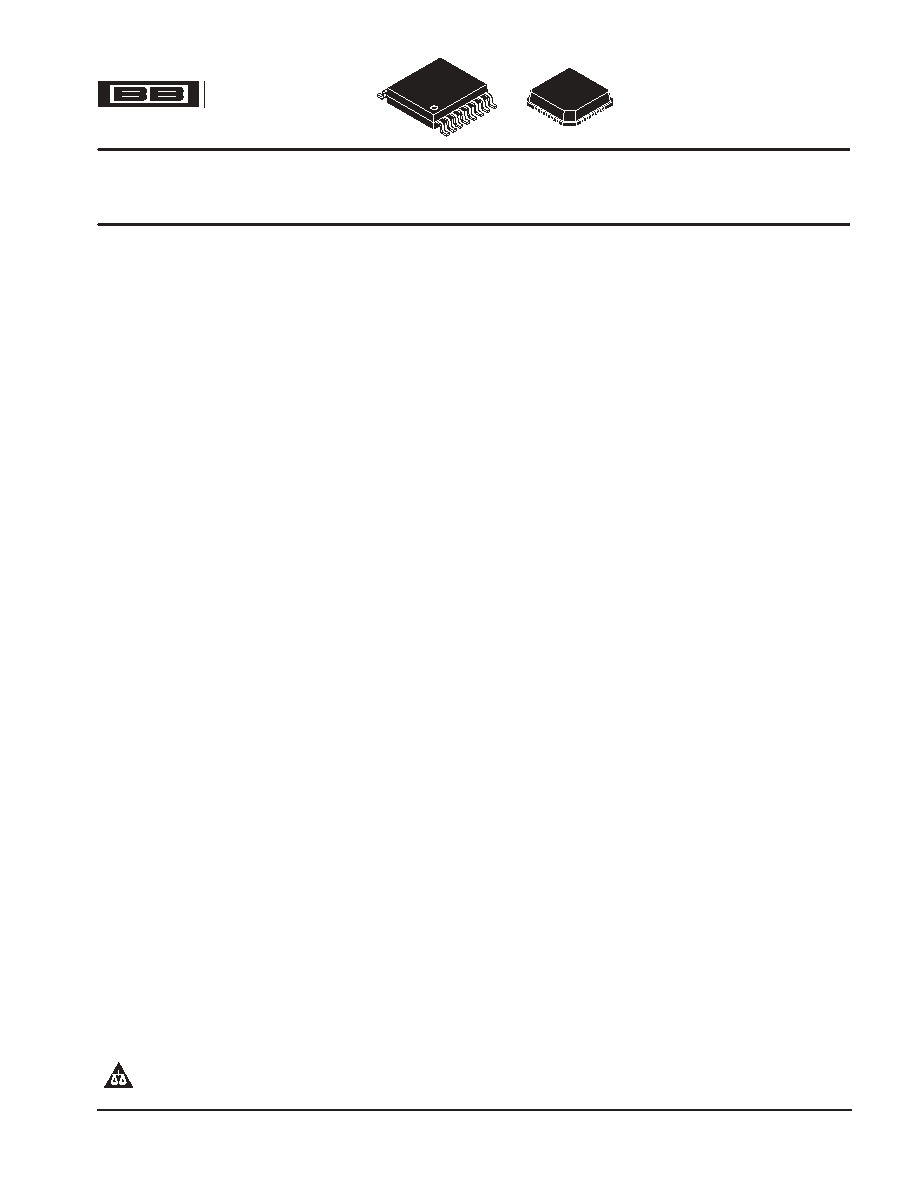
Packages: TSSOP-16 and VQFN-20, Lead Free
APPLICATIONS
D
Portable Audio Player
D
Cellular Phone
D
PDA
D
Other Applications Requiring Low-Voltage
Operation
DESCRIPTION
The PCM1770 and PCM1771 devices are CMOS,
monolithic, integrated circuits which include stereo
digital-to-analog converters, headphone circuitry, and
support circuitry in small TSSOP-16 and VQFN-20
packages.
The data converters use TI's enhanced multilevel
-
architecture, which employs noise shaping and
multilevel amplitude quantization to achieve excellent
dynamic performance and improved tolerance to clock
jitter. The PCM1770 and PCM1771 devices accept
several industry standard audio data formats with 16- to
24-bit data, left-justified, I
2
S, etc., providing easy
interfacing to audio DSP and decoder devices.
Sampling rates up to 50 kHz are supported. A full set of
user-programmable functions are accessible through a
3-wire serial control port, which supports register write
functions.
PRODUCTION DATA information is current as of publication date. Products
conform to specifications per the terms of Texas Instruments standard warranty.
Production processing does not necessarily include testing of all parameters.
Please be aware that an important notice concerning availability, standard warranty, and use in critical applications of Texas Instruments
semiconductor products and disclaimers thereto appears at the end of this data sheet.
Burr Brown Products
from Texas Instruments
Copyright
2004, Texas Instruments Incorporated
PCM1770
PCM1771
SLES011C ≠ SEPTEMBER 2001 ≠ REVISED MAY 2004
www.ti.com
2
These devices have limited built-in ESD protection. The leads should be shorted together or the device placed in conductive foam during
storage or handling to prevent electrostatic damage to the MOS gates.
PACKAGE/ORDERING INFORMATION
PRODUCT
PACKGE
PACKAGE
PACKAGE
CODE
OPERATION
TEMPERATURE
RANGE
PACKAGE
MARKING
ORDERING
NUMBER
TRANSPORT
MEDIA
PCM1770PW
16-lead TSSOP
16PW
-25
∞
C to 85
∞
C
PCM1770
PCM1770PW
Tube
PCM1770PW
16-lead TSSOP
16PW
-25
∞
C to 85
∞
C
PCM1770
PCM1770PWR
Tape and reel
PCM1770RGA
20-lead VQFN
20RGA
-25
∞
C to 85
∞
C
PCM1770
PCM1770RGA
Tray
PCM1770RGA
20-lead VQFN
20RGA
-25
∞
C to 85
∞
C
PCM1770
PCM1770RGAR
Tape and reel
PCM1771PW
16-lead TSSOP
16PW
-25
∞
C to 85
∞
C
PCM1771
PCM1771PW
Tube
PCM1771PW
16-lead TSSOP
16PW
-25
∞
C to 85
∞
C
PCM1771
PCM1771PWR
Tape and reel
PCM1771RGA
20-lead VQFN
20RGA
-25
∞
C to 85
∞
C
PCM1771
PCM1771RGA
Tray
PCM1771RGA
20-lead VQFN
20RGA
-25
∞
C to 85
∞
C
PCM1771
PCM1771RGAR
Tape and reel
ABSOLUTE MAXIMUM RATINGS
over operating free-air temperature range unless otherwise noted(1)
PCM1770
PCM1771
Supply voltage: VCC, VHP
4 V
Supply voltage differences: VCC, VHP
±
0.1 V
Ground voltage differences
±
0.1 V
Digital input voltage
≠0.3 V to 4.0 V
Input current (any terminals except supplies)
±
10 mA
Operating temperature
≠40
∞
C to 125
∞
C
Storage temperature
≠55
∞
C to 150
∞
C
Junction temperature
150
∞
C
Lead temperature (soldering)
260
∞
C, 5 s
Package temperature (IR reflow, peak)
260
∞
C
(1) Stresses beyond those listed under "absolute maximum ratings" may cause permanent damage to the device. These are stress ratings only, and
functional operation of the device at these or any other conditions beyond those indicated under "recommended operating conditions" is not
implied. Exposure to absolute-maximum-rated conditions for extended periods may affect device reliability.
PCM1770
PCM1771
SLES011C ≠ SEPTEMBER 2001 ≠ REVISED MAY 2004
www.ti.com
3
ELECTRICAL CHARACTERISTICS
all specifications at TA = 25
∞
C, VCC = VHP = 2.4 V, fS = 44.1 kHz, system clock = 256 fS and 24-bit data, RL = 16
, unless otherwise noted
PARAMETER
TEST CONDITIONS
PCM1770PW, PCM1771PW,
PCM1770RGA, PCM1771RGA
UNIT
PARAMETER
TEST CONDITIONS
MIN
TYP
MAX
UNIT
Resolution
24
Bits
OPERATING FREQUENCY
Sampling frequency (fS)
5
50
kHz
System clock frequency
128f S, 192 fS, 256 fS, 384 fS
DIGITAL INPUT/OUTPUT(1)(2)
VIH
Input logic level
0.7 VCC
Vdc
VIL
Input logic level
0.3 VCC
Vdc
IIH
Input logic current
VIN = VCC
10
µ
A
IIL
Input logic current
VIN = 0 V
≠10
µ
A
VOH
Output logic level(3)
IOH = ≠2 mA
0.7 VCC
Vdc
VOL
Output logic level(3)
IOL = 2 mA
0.3 VCC
Vdc
DYNAMIC PERFORMANCE (HEADPHONE OUTPUT)
Full scale output voltage
0 dB
0.55 VHP
VP-P
Dynamic range
EIAJ, A-weighted
90
98
dB
Signal-to-noise ratio
EIAJ, A-weighted
90
98
dB
THD+N
0 dB (13 mW)
0.1%
THD+N
-20 dB (0.1 mW)
0.04%
0.1%
Output power
Stereo
10
13
mWrms
Output power
Monaural
20
26
mWrms
Channel separation
64
72
dB
Load resistance
14
16
DC ACCURACY
Gain error
±
2
±
8
% of FSR
Gain mismatch,
channel-to-channel
±
2
±
8
% of FSR
Bipolar zero error
VOUT = 0.5 VCC at BPZ
±
30
±
75
mV
ANALOG LINE INPUT (MIXING CIRCUIT)
Analog input voltage range
0.584 VHP
VP-P
Gain (analog input to headphone
output)
0.67
Analog input impedance
10
k
THD+N
AIN = 0.56 VHP (peak-to-peak)
0.1%
DIGITAL FILTER PERFORMANCE
Pass band
0.454 fS
Stop band
0.546 fS
Pass-band ripple
±
0.04
dB
Stop-band attenuation
≠50
dB
Group delay
20/fS
44.1-kHz de-emphasis error
±
0.1
dB
(1) Digital inputs and outputs are CMOS compatible.
(2) All logic inputs are 3.3-V tolerant and not terminated internally.
(3) LRCK and BCK terminals
PCM1770
PCM1771
SLES011C ≠ SEPTEMBER 2001 ≠ REVISED MAY 2004
www.ti.com
4
ELECTRICAL CHARACTERISTICS(continued)
all specifications at TA = 25
∞
C, VCC = VHP = 2.4 V, fS = 44.1 kHz, system clock = 256 fS and 24-bit data, RL = 16
, unless otherwise noted
PARAMETER
TEST CONDITIONS
PCM1770PW, PCM1771PW,
PCM1770RGA, PCM1771RGA
UNIT
PARAMETER
TEST CONDITIONS
MIN
TYP
MAX
UNIT
ANALOG FILTER PERFORMANCE
Frequency response
at 20 kHz
±
0.2
dB
POWER SUPPLY REQUIREMENTS
Voltage range, VCC, VHP
1.6
2.4
3.6
Vdc
ICC
BPZ input
1.5
2.5
mA
IHP
Supply current
BPZ input
1.2
2.5
mA
ICC +
IHP
Supply current
Power down(1)
5
15
µ
A
Power dissipation
BPZ input
6.5
12
mW
Power dissipation
Power down(1)
12
36
µ
W
TEMPERATURE RANGE
Operation temperature
≠25
85
∞
C
PCM1770PW, -71PW: 16-terminal TSSOP
150
JA
Thermal resistance
PCM1770RGA, -71RGA: 20-terminal
VQFN
130
∞
C/W
(1) All input signals are held static.
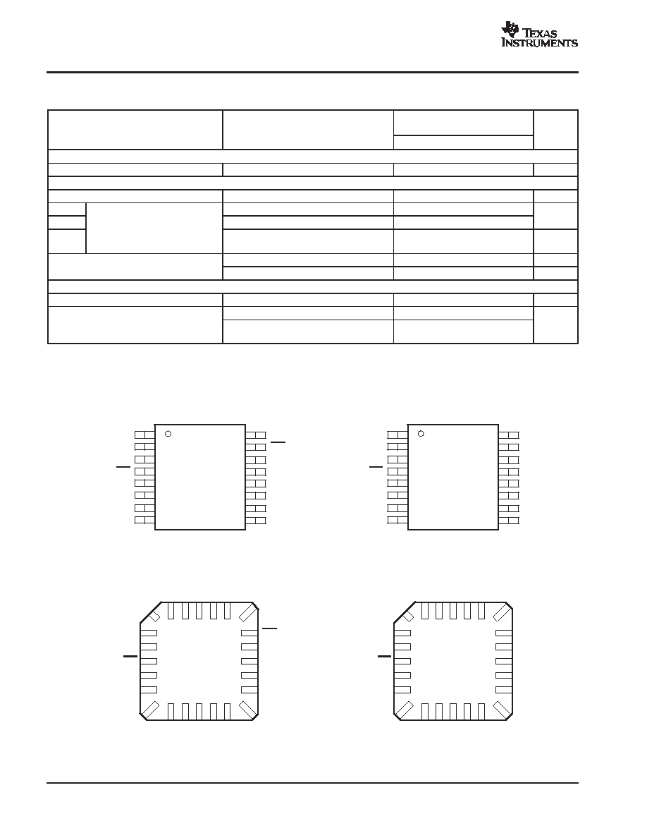
PIN ASSIGNMENTS
1
2
3
4
5
6
7
8
16
15
14
13
12
11
10
9
LRCK
DATA
BCK
PD
AGND
HGND
V
COM
H
OUT
R
SCKI
MS
MC
MD
V
CC
V
HP
AIN
H
OUT
L
PCM1770
PW PACKAGE
(TOP VIEW)
1
2
3
4
5
6
7
8
16
15
14
13
12
11
10
9
LRCK
DATA
BCK
PD
AGND
HGND
V
COM
H
OUT
R
SCKI
FMT
AMIX
DEMP
V
CC
V
HP
AIN
H
OUT
L
PCM1771
PW PACKAGE
(TOP VIEW)
PCM1770
RGA PACKAGE
(TOP VIEW)
DATA
BCK
PD
AGND
HGND
LRCK
NC
NC
NC
SCKI
COM
NC
AIN
V
R
OUT
H
L
OUT
H
NC - No internal connection
FMT
AMIX
DEMP
VCC
VHP
PCM1771
RGA PACKAGE
(TOP VIEW)
DATA
BCK
PD
AGND
HGND
LRCK
NC
NC
NC
SCKI
COM
NC
AIN
V
MS
MC
MD
V
CC
V
HP
1
2
3
4
5
15
14
13
12
11
6
7
8
9 10
20 19 18 17 16
R
OUT
H
L
OUT
H
1
2
3
4
5
15
14
13
12
11
6
7
8
9 10
20 19 18 17 16
PCM1770
PCM1771
SLES011C ≠ SEPTEMBER 2001 ≠ REVISED MAY 2004
www.ti.com
5
Terminal Functions
PCM1770PW
TERMINAL
I/O
DESCRIPTIONS
NAME
NO.
I/O
DESCRIPTIONS
AGND
5
≠
Analog ground. This is a return for VCC.
AIN
10
I
Monaural analog signal mixer input. The signal can be mixed with the output of L- and R-channel DACs.
BCK
3
I/O
Serial bit clock. Clocks the individual bits of the audio data input, DATA. In the slave interface mode, this clock is input
from external device. In the master interface mode, the PCM1770 device generates the BCK output to external device.
DATA
2
I
Serial audio data input
HGND
6
≠
Analog ground. This is a return for VHP.
HOUTL
9
O
L-channel analog signal output of the headphone amplifiers
HOUTR
8
O
R-channel analog signal output of the headphone amplifiers
LRCK
1
I/O
Left and right clock. Determines which channel is being input on the audio data input, DATA. The frequency of LRCK
must be the same as the audio sampling rate. In the slave interface mode, this clock is input from an external device.
In the master interface mode, the PCM1770 device generates the LRCK output to an external device.
MC
14
I
Mode control port serial bit clock input. Clocks the individual bits of the control data input, MD.
MD
13
I
Mode control port serial data input. Controls the operation mode on the PCM1770 device.
MS
15
I
Mode control port select. The control port is active when this terminal is low.
PD
4
I
Reset input. When low, the PCM1770 device is powered down, and all mode control registers are reset to default
settings.
SCKI
16
I
System clock input
VCC
12
≠
Power supply for all analog circuits except the headphone amplifier.
VCOM
7
≠
Decoupling capacitor connection. An external 10-
µ
F capacitor connected from this terminal to analog ground is
required for noise filtering. Voltage level of this terminal is 0.5VHP nominal.
VHP
11
≠
Analog power supply for the headphone amplifier circuits. The voltage level must be the same as VCC.
PCM1770RGA
TERMINAL
I/O
DESCRIPTIONS
NAME
NO.
I/O
DESCRIPTIONS
AGND
4
≠
Analog ground. This is a return for VCC.
AIN
10
I
Monaural analog signal mixer input. The signal can be mixed with output of L- and R-channel DACs.
BCK
2
I/O
Serial bit clock. Clocks the individual bits of the audio data input, DATA. In the slave interface mode, this clock is input
from external device. In the master interface mode, the PCM1770 device generates the BCK output to external
device.
DATA
1
I
Serial audio data input
HGND
5
≠
Analog ground. This is a return for VHP.
HOUTL
9
O
L-channel analog signal output of the headphone amplifiers
HOUTR
7
O
R-channel analog signal output of the headphone amplifiers
LRCK
20
I/O
Left and right clock. Determines which channel is being input on the audio data input, DATA. The frequency of LRCK
must be the same as the audio sampling rate. In the slave interface mode, this clock is input from an external device.
In the master interface mode, the PCM1770 device generates the LRCK output to an external device.
MC
14
I
Mode control port serial bit clock input. Clocks the individual bits of the control data input, MD.
MD
13
I
Mode control port serial data input. Controls the operation mode on the PCM1770 device.
MS
15
I
Mode control port select. The control port is active when this terminal is low.
NC
8, 17,
18, 19
≠
No connect
PD
3
I
Reset input. When low, the PCM1770 device is powered down, and all mode control registers are reset to default
settings.
SCKI
16
I
System clock input
VCC
12
≠
Power supply for all analog circuits except the headphone amplifier.
VCOM
6
≠
Decoupling capacitor connection. An external 10-
µ
F capacitor connected from this terminal to analog ground is
required for noise filtering. Voltage level of this terminal is 0.5VHP nominal.
VHP
11
≠
Analog power supply for the headphone amplifier circuits. The voltage level must be the same as VCC.