Document Outline
- Features
- Description
- Ordering Information
- Pin-Out Information
- Standard Application
- Specifications
- Typical Characteristics
- Application Notes
- Operating Features of the PT3400 Series of Isolated DC/ DC Converters
- Under-Voltage Lockout
- Over-Current Protection
- Primary-Secondary Isolation
- Input Current Limiting
- Thermal Considerations
- Adjusting the Output Voltage of the 30W-Rated PT3400 Series of Isolated \
DC/ DC Converters
- Using the On/Off Enable Controls on the PT3400 Series of DC/ DC Converte\
rs
- Automatic (UVLO) Power-Up
- Positive Output Enable (Negative Inhibit)
- Negative Output Enable (Positive Inhibit)
- On/Off Enable Turn-On Time
- Using the Power-Up Sequencing Feature of the PT3400 Series of DC/ DC Con\
verters
- Introduction
- Configuration for Power-up Sequencing
- IMPORTANT NOTICE
For technical support and more information, see inside back cover or visit www.ti.com
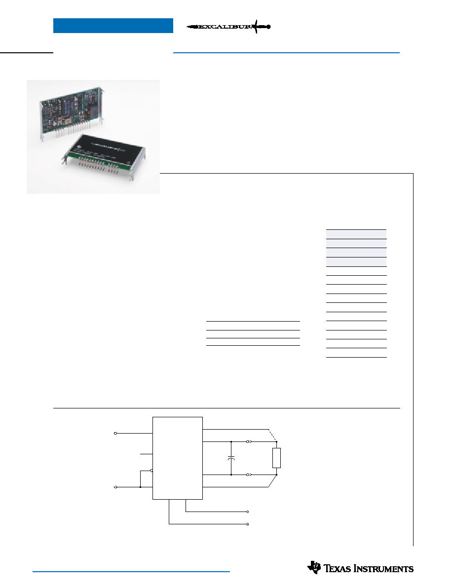
Standard Application
Features
∑
Input Voltage Range:
36V to 75V
∑
35W Output Power
∑
90% Efficiency
∑
1500 VDC Isolation
∑
Low Profile (8 mm)
∑
Adjustable Output Voltage
∑
Dual-Logic On/Off Enable
∑
Power-Up Sequence Control
PT3400 Series
35-W 48-V Input Isolated
DC/DC Converter
SLTS164B - JULY 2002 - REVISED OCTOBER 2002
Ordering Information
PT3401
H = 3.3V/10A (33W)
PT3402
H = 2.5V/12A (30W)
PT3403
H = 1.8V/12A (21.6W)
PT3404
H = 1.5V/16A (24W)
PT3405
H = 1.4V/16A (22.4W)
PT3406
H = 1.2V/16A (19.2W)
PT3407
H = 1V/16A
(16W)
PT3408
H = 5V/7A
(35W)
Pin-Out Information
Pin Function
1
EN 1
2
EN 2*
3
≠V
in
4
+V
in
5
SEQ
6
V
out
Adj
7
≠V
sense
8
≠V
out
9
≠V
out
10 ≠V
out
11 +V
out
12 +V
out
13 +V
out
14 +V
sense
* Negative logic
Shaded functions indicate those
pins that are referenced to ≠V
in
.
Description
The PT3400 ExcaliburTM power modules
are a series of 35-W rated DC/DC converters
housed in a low-profile space-saving copper
case. Fully isolated for telecom applications,
the series includes a number of standard volt-
ages, including 1.0 VDC. Other applications
include industrial, high-end computing, and
other distributed power applications that
require input-to-output isolation.
PT3400 modules incorporate a feature
that simplifies the design of multiple voltage
power supplies in DSP and ASIC applications.
Using the SEQ control pin, the output voltage
of two PT3400 modules in a power supply
system can be made to self sequence at power-
up. Other features include output voltage
adjust, over-current protection, input under-
voltage lockout, and a differential remote
sense to compensate for any voltage drop
between the converter and load.
∑
Differential Remote Sense
∑
Over-Current Protection
∑
Space Saving Package
∑
Solderable Copper Case
∑
Safety Approvals Pending
PT Series Suffix
(PT1234
x
)
Case/Pin
Order
Package
Configuration
Suffix
Code
Vertical
N
(EPL)
Horizontal
A
(EPM)
SMD
C
(EPN)
(Reference the applicable package code draw-
ing for the dimensions and PC board layout)
L
O
A
D
* Remote Sense (≠)
Remote Sense (+)
+V
OUT
≠V
OUT
V
O
Adj
+V
IN
≠V
IN
SEQ
C
OUT
330µF
+
PT3400
1
2
11≠13
8≠10
14
7
3
4
≠V
IN
+V
IN
EN 1
EN 2
SEQ
V
o
Adj
6
5
+V
OUT
≠V
OUT
+V
SENSE
≠V
SENSE
An output capacitor is required on models
with an output voltage less than 2.5V.
* ≠V
sense
(pin 7) must be connected to -V
out
,
either at the load or directly to pin 8 of the
converter.

For technical support and more information, see inside back cover or visit www.ti.com
PT3400 Series
35-W 48-V Input Isolated
DC/DC Converter
SLTS164B - JULY 2002 - REVISED OCTOBER 2002
Specifications
(Unless otherwise stated, T
a
=25∞C, V
in
=48V, C
in
=0µF, I
o
=I
o
max, and C
out
as required)
PT3400 Series
Characteristic
Symbol
Conditions
Min
Typ
Max
Units
Output Current
I
o
Over V
in
range
V
o
1.5V
0
--
16
V
o
=
1.8V/2.5V
0
--
12
A
V
o
=
3.3V
0
--
10
V
o
=
5V
0
--
7
Input Voltage Range
V
in
Over I
o
Range
36
48
75
VDC
Set Point Voltage Tolerance
V
o
tol
--
±1
±2
%V
o
Temperature Variation
Reg
temp
≠40∞
T
a
+85∞C, I
o
=I
o
min
--
±0.8
--
%V
o
Line Regulation
Reg
line
Over V
in
range
V
o
=
5.0V
--
±5
±20
mV
V
o
3.3V
--
±5
±15
mV
Load Regulation
Reg
load
Over I
o
range
V
o
=
5.0V
--
±1
±15
(1)
mV
V
o
3.3V
--
±1
±10
(1)
mV
Total Output Voltage Variation
V
o
tot
Includes set-point, line, load,
--
±2
±3
%V
o
≠40∞
T
a
+85∞C
Efficiency
I
o
=70% of I
o
max
V
o
=
5V
--
91
--
V
o
=
3.3V
--
90
--
V
o
=
2.5V
--
89
--
V
o
=
1.8V
--
85
--
%
V
o
=
1.5V
--
84
--
V
o
=
1.4V
--
84
--
V
o
=
1.2V
--
82
--
V
o
=
1V
--
80
--
V
o
Ripple (pk-pk)
V
r
20MHz bandwidth
V
o
3.3V
--
50
--
mV
pp
V
o
2.5V
--
25
--
Transient Response
t
tr
0.1A/µs load step, 50% to 75% I
o
max
--
100
--
µs
V
tr
V
o
over/undershoot
--
±4
--
%V
o
Output Adjust
V
adj
V
o
2.5V
≠5
--
+5
%V
o
V
o
1.8V
≠0
--
+10
Over-Current Threshold
I
TRIP
V
in
=36V
V
o
=
5.0V
--
9
--
V
o
=
3.3V
--
12.5
--
V
o
=
2.5V/1.8V
--
16
--
A
V
o
1.5V
--
20
--
Switching Frequency
s
Over V
in
range
250
300
350
kHz
Under-Voltage Lockout
UVLO
Rising
--
34
--
V
Falling
--
32
--
Enable On/Off (Pins 1, 2)
Referenced to ≠V
in
(pin 3)
Input High Voltage
V
IH
5
--
Open
(2)
V
Input Low Voltage
V
IL
≠0.3
--
+0.4
Input Low Current
I
IL
--
0.5
--
mA
Standby Input Current
I
in
standbypins 1 & 3 connected
--
5
--
mA
Internal Input Capacitance
C
in
--
1.0
--
µF
External Output Capacitance
C
out
V
o
=
1.0V
470
(3)
--
TBD
V
o
1.8V
330
(3)
--
TBD
µF
V
o
2.5V
0
--
TBD
Isolation Voltage
Input≠output/input≠case
1500
--
--
V
Capacitance
Input to output
--
1500
--
pF
Resistance
Input to output
10
--
--
M
Operating Temperature Range
T
a
Over V
in
range
≠40
(4)
--
85
(5)
∞C
Solder Reflow Temperature
T
reflow
Surface temperature of module pins or case
--
--
215
(6)
∞C
Storage Temperature
T
s
--
≠40
--
125
∞C
ReliabilityMTBF
Per Bellcore TR-332
2.8
--
--
10
6
Hrs
50% stress, T
a
=40∞C, ground benign
Mechanical Shock
--
Per Mil-Std-883D, method 2002.3,
--
TBD
--
G's
1mS, half-sine, mounted to a fixture
Mechanical Vibration
--
Mil-Std-883D, Method 2007.2,
Vertical
--
TBD
(7)
--
G's
20-2000Hz, PCB mounted
Horizontal
--
TBD
(7)
--
Weight
--
--
--
34
--
grams
Flammability--
Materials meet UL 94V-0
Notes:
(1) If the remote sense feature is not being used, ≠V
sense
(pin 7) must be connected to ≠V
out
(pin 8).
(2) The On/Off Enable inputs (pins 1 & 2) have internal pull-ups. They may either be connected to ≠V
in
or left open circuit. Leaving pin 1 open-circuit and
connecting pin 2 to ≠V
in
allows the the converter to operate when input power is applied. The maximum open-circuit voltage of the Enable pins is 10V.
(3) An output capacitor is required for proper operation for all models in which the output voltage is 1.8VDC or less. For models with an output voltage of
2.5V or higher an output capacitor is optional.
(4) For operation below 0∞C, Cout must have stable characteristics. Use low ESR tantalum capacitors, or capacitors with a polymer type dielectric.
(5) See Safe Operating Area curves or contact the factory for the appropriate derating.
(6) During reflow of SMD package version do not elevate the module case, pins, or internal component temperatures above a peak of 215∞C. For further
guidance refer to the application note, "Reflow Soldering Requirements for Plug-in Surface Mount Products," (SLTA051).
(7) The case pins on through-hole pin configurations (N & A) must be soldered. For more information see the applicable package outline drawing.

For technical support and more information, see inside back cover or visit www.ti.com
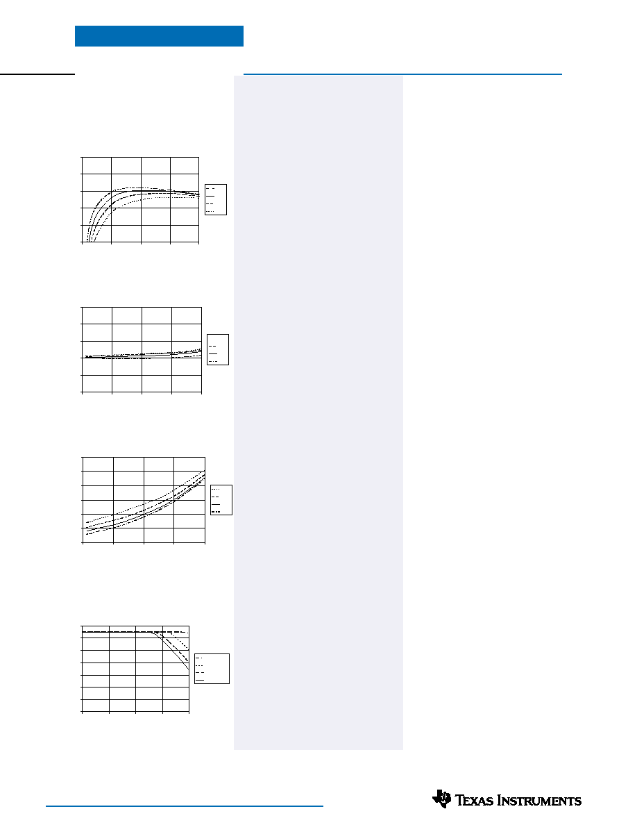
Note A:
Characteristic data has been developed from actual products tested at 25∞C. This data is considered typical data for the Converter.
Note B:
SOA curves represent the conditions at which internal components are at or below the manufacturer's maximum operating temperatures
Efficiency vs Output Current
Ripple vs Output Current
Power Dissipation vs Output Current
PT3408, 5VDC
(See Note A)
Typical Characteristics
PT3400 Series
35-W 48-V Input Isolated
DC/DC Converter
PT3401, 3.3 VDC
(See Note A)
PT3402, 2.5 VDC
(See Note A)
Efficiency vs Output Current
Ripple vs Output Current
Power Dissipation vs Output Current
Efficiency vs Output Current
Ripple vs Output Current
Power Dissipation vs Output Current
Safe Operating Area
(See Note B)
PT3401; V
IN
=60V
Safe Operating Area
(See Note B)
PT3408; V
IN
=60V
Safe Operating Area
(See Note B)
PT3402; V
IN
=60V
20
30
40
50
60
70
80
90
0
2
4
6
8
10
Iout (A)
Ambient Temperature (∞C)
200LFM
120LFM
60LFM
Nat conv
Airflow
20
30
40
50
60
70
80
90
0
2
4
6
8
10
12
Iout (A)
Ambient Temperature (
∞
C)
200LFM
120LFM
60LFM
Nat conv
Airflow
50
60
70
80
90
100
0
1
2
3
4
5
6
7
Iout (A)
Efficiency - %
36.0V
48.0V
60.0V
75.0V
V
IN
0
10
20
30
40
50
0
1
2
3
4
5
6
7
Iout (A)
Ripple - mV
75.0V
60.0V
48.0V
36.0V
V
IN
0
1
2
3
4
5
6
0
1
2
3
4
5
6
7
Iout (A)
Pd - Watts
75.0V
60.0V
48.0V
36.0V
V
IN
20
30
40
50
60
70
80
90
0
1
2
3
4
5
6
7
Iout (A)
Ambient Temperature (
∞
C)
200LFM
120LFM
60LFM
Nat conv
Airflow
50
60
70
80
90
100
0
2
4
6
8
10
Iout (A)
Efficiency - %
36.0V
48.0V
60.0V
75.0V
V
IN
0
10
20
30
40
50
0
2
4
6
8
10
Iout (A)
Ripple - mV
75.0V
60.0V
48.0V
36.0V
V
IN
0
1
2
3
4
5
6
0
2
4
6
8
10
Iout (A)
Pd - Watts
75.0V
60.0V
48.0V
36.0V
V
IN
50
60
70
80
90
100
0
2
4
6
8
10
12
Iout (A)
Efficiency - %
36.0V
48.0V
60.0V
75.0V
V
IN
0
10
20
30
40
50
0
2
4
6
8
10
12
Iout (A)
Ripple - mV
75.0V
60.0V
48.0V
36.0V
V
IN
0
1
2
3
4
5
6
0
2
4
6
8
10
12
Iout (A)
Pd - Watts
75.0V
60.0V
48.0V
36.0V
V
IN
SLTS164B - JULY 2002 - REVISED OCTOBER 2002

For technical support and more information, see inside back cover or visit www.ti.com
PT3403, 1.8 VDC
(See Note A)
PT3400 Series
35-W 48-V Input Isolated
DC/DC Converter
Typical Characteristics
PT3404/5, 1.5/1.4 VDC
(See Note A)
PT3406, 1.2 VDC
(See Note A)
Note A:
Characteristic data has been developed from actual products tested at 25∞C. This data is considered typical data for the Converter.
Note B:
SOA curves represent the conditions at which internal components are at or below the manufacturer's maximum operating temperatures
Efficiency vs Output Current
Ripple vs Output Current
Power Dissipation vs Output Current
Efficiency vs Output Current
Ripple vs Output Current
Power Dissipation vs Output Current
Efficiency vs Output Current
Ripple vs Output Current
Power Dissipation vs Output Current
Safe Operating Area
(See Note B)
PT3404; V
IN
=60V
Safe Operating Area
(See Note B)
PT3403; V
IN
=60V
Safe Operating Area
(See Note B)
PT3406; V
IN
=60V
0
5
10
15
20
25
0
4
8
12
16
Iout (A)
Ripple - mV
75.0V
60.0V
48.0V
36.0V
V
IN
50
60
70
80
90
100
0
4
8
12
16
Iout (A)
Efficiency - %
36.0V
48.0V
60.0V
75.0V
V
IN
0
1
2
3
4
5
6
0
4
8
12
16
Iout (A)
Pd - Watts
75.0V
60.0V
48.0V
36.0V
V
IN
50
60
70
80
90
100
0
3
6
9
12
Iout (A)
Efficiency - %
36.0V
48.0V
60.0V
75.0V
V
IN
0
10
20
30
40
50
0
3
6
9
12
Iout (A)
Ripple - mV
75.0V
60.0V
48.0V
36.0V
V
IN
0
1
2
3
4
5
6
0
3
6
9
12
Iout (A)
Pd - Watts
75.0V
60.0V
48.0V
36.0V
V
IN
50
60
70
80
90
100
0
4
8
12
16
Iout (A)
Efficiency - %
36.0V
48.0V
60.0V
75.0V
V
IN
0
5
10
15
20
25
0
4
8
12
16
Iout (A)
Ripple - mV
75.0V
60.0V
48.0V
36.0V
V
IN
0
1
2
3
4
5
6
0
4
8
12
16
Iout (A)
Pd - Watts
75.0V
60.0V
48.0V
36.0V
V
IN
20
30
40
50
60
70
80
90
0
4
8
12
16
Iout (A)
Ambient Temperature (
∞
C)
200LFM
120LFM
60LFM
Nat conv
Airflow
20
30
40
50
60
70
80
90
0
4
8
12
16
Iout (A)
Ambient Temperature (
∞
C)
200LFM
120LFM
60LFM
Nat conv
Airflow
20
30
40
50
60
70
80
90
0
2
4
6
8
10
12
Iout (A)
Ambient Temperature (
∞
C)
200LFM
120LFM
60LFM
Nat conv
Airflow
SLTS164B - JULY 2002 - REVISED OCTOBER 2002
For technical support and more information, see inside back cover or visit www.ti.com
PT3400 Series
35-W 48-V Input Isolated
DC/DC Converter
Typical Characteristics
50
60
70
80
90
100
0
4
8
12
16
Iout (A)
Efficiency - %
36V
48V
60V
75V
V
IN
PT3407, 1.0 VDC
(See Note A)
Efficiency vs Output Current
Ripple vs Output Current
Power Dissipation vs Output Current
Safe Operating Area
(See Note B)
PT3406; V
IN
=60V
0
5
10
15
20
25
0
4
8
12
16
Iout (A)
Ripple - mV
75V
60V
48V
36V
V
IN
0
1
2
3
4
5
6
0
4
8
12
16
Iout (A)
Pd - Watts
75V
60V
48V
36V
V
IN
20
30
40
50
60
70
80
90
0
4
8
12
16
Iout (A)
Ambient Temperature (
∞
C)
200LFM
120LFM
60LFM
Nat conv
Airflow
SLTS164B - JULY 2002 - REVISED OCTOBER 2002
Note A:
Characteristic data has been developed from actual products tested at 25∞C. This data is considered typical data for the Converter.
Note B:
SOA curves represent the conditions at which internal components are at or below the manufacturer's maximum operating temperatures
For technical support and more information, see inside back cover or visit www.ti.com
Operating Features of the PT3400 Series
of Isolated DC/DC Converters
Under-Voltage Lockout
An Under-Voltage Lock-Out (UVLO) inhibits the opera-
tion of the converter until the input voltage is above the
UVLO threshold (see the data sheet specification). Below
this voltage, the module's output is held off, irrespective
of the state of either the EN1 & EN2 enable controls.
The UVLO allows the module to produce a clean transi-
tion during both power-up and power-down, even when
the input voltage is rising or falling slowly. It also reduces
the high start-up current during normal power-up of the
converter, and minimizes the current drain from the
input source during low-input voltage conditions. The
UVLO threshold includes about 1V of hysteresis.
If EN2 (pin 2) is connected to -V
in
(pin 3) and EN1 (pin 1)
is left open, the module will automatically power up when
the input voltage rises above the UVLO threshold (see
data sheet `Standard Application' schematic). Once
operational, the converter will conform to its operating
specifications when the minimum specified input voltage
is reached.
Over-Current Protection
To protect against load faults, the PT3400 series incor-
porates output over-current protection. Applying a load
that exceeds the converter's over-current threshold (see
applicable specification) will cause the regulated output
to shut down. Following shutdown the module will peri-
odically attempt to automatically recover by initiating a
soft-start power-up. This is often described as a "hiccup"
mode of operation, whereby the module continues in the
cycle of succesive shutdown and power up until the load
fault is removed. Once the fault is removed, the converter
then automatically recovers and returns to normal op-
eration.
Primary-Secondary Isolation
Electrical isolation is provided between the input termi-
nals (primary) and the output terminals (secondary). All
converters are production tested to a primary-secondary
withstand voltage of 1500VDC. This specification com-
plies with UL60950 and EN60950 and the requirements
for operational isolation. Operational isolation allows these
converters to be configured for either a positive or negative
input voltage source. The data sheet `Pin-Out Information'
uses shading to indicate which pins are associated with the
primary. They include pins 1 through 4, inclusive.
Input Current Limiting
The converter is not internally fused. For safety and
overall system protection, the maximum input current to
the converter must be limited. Active or passive current
limiting can be used. Passive current limiting can be a
fast acting fuse. A 125-V fuse, rated no more than 5A, is
recommended. Active current limiting can be imple-
mented with a current limited "Hot-Swap" controller.
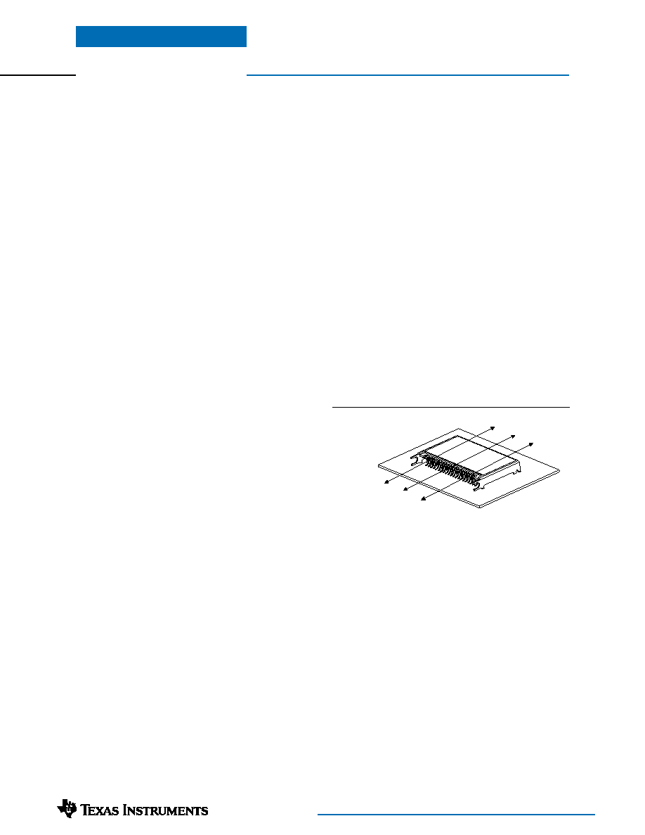
Thermal Considerations
Airflow may be necessary to ensure that the module can
supply the desired load current in environments with
elevated ambient temperatures. The required airflow
rate may be determined from the Safe Operating Area
(SOA) thermal derating chart (see converter specifica-
tions). The recommended direction for airflow is into the
longest side of the module's metal case. See Figure 1-1.
Figure 1-1
PT3400 Series
Recommended direction for airflow is
into (perpendicular to) the longest side
Application Notes
Application Notes
For technical support and more information, see inside back cover or visit www.ti.com
Adjusting the Output Voltage of the 30W-Rated
PT3400 Series of Isolated DC/DC Converters
The output voltage of the PT3400 ExcaliburTM series of
isolated DC/DC converters may be adjusted over a limited
range from the factory-trimmed nominal value. Adjust-
ment is accomplished with a single external resistor. The
placement the resistor determines the direction of adjust-
ment, either up or down, and the value of the resistor the
magnitude of adjustment. Table 3-1 gives the allowable
adjustment range for each model in the series as V
a
(min)
and V
a
(max) respectively. Note that converters with an
output voltage of 1.8V or less can only be adjusted up
1
.
Adjust Up:
An increase in the output voltage is obtained
by adding a resistor, R
1
between V
o
Adj (pin 6), and ≠V
sense
(pin 7).
Adjust Down
(PT3401, PT3402, & PT3408 Only):
Add a
resistor
(R
2
)
, between V
o
Adj (pin 6) and +V
sense
(pin 14).
Refer to Figure 3-1 and Table 3-2 for both the placement and
value of the required resistor, R
1
or
(R
2
)
.
The values of R
1
[adjust up], and
(R
2
)
[adjust down], can
also be calculated using the following formulas.
R
1
=
2 ∑ R
o
≠ R
s
k
V
a
≠ V
o
(R
2
)
=
R
o
(V
a
≠ 2)
≠ R
s
k
V
o
≠ V
a
Where, V
a
= Adjusted output voltage
V
o
= Original output voltage
R
o
= Resistor constant in Table 3-1
R
s
= Internal series resistance in Table 3-1
Figure 3-1
Notes:
1. The output voltage of the PT3401 (3.3V),
PT3402 (2.5V), and PT3408 (5V) may be adjusted either
higher or lower. All other models, which have an output
voltage of 1.8V or less, can only be adjusted higher.
2. Use only a single 1% resistor in either the R
1
or
(R
2
)
location. Place the resistor as close to the converter as
possible.
3. Never connect capacitors to V
o
Adj. Any capacitance added
to this pin will affect the stability of the converter.
4. If the output voltage is increased, the maximum load
current must be derated according to the following
equation.
I
o
(max)
= V
o
◊
I
o
(rated)
V
a
In any instance, the load current must not exceed the
converter's rated output current I
o
(rated) in Table 3-1.
PT3400 Series
L
O
A
D
* Remote Sense (≠)
Remote Sense (+)
+V
OUT
≠V
OUT
+V
IN
≠V
IN
C
OUT
330µF
+
R
1
A d j u s t U p
(R
2
)
Adj Down
PT3400
1
2
11≠13
8≠10
14
7
3
4
≠V
IN
+V
IN
EN 1
EN 2
SEQ
V
o
Adj
6
5
+V
OUT
≠V
OUT
+V
SENSE
≠V
SENSE
For technical support and more information, see inside back cover or visit www.ti.com
Application Notes
continued
Table 3-2
DC/DC CONVERTER ADJUSTMENT RESISTOR VALUES
Series Pt #
PT3408
PT3401
PT3402
PT3403
PT3404
PT3405
PT3406
PT3407
V
o
(nom)
5V
3.3V
2.5V
1.8V
1.5V
1.4V
1.2V
1.0V
V
a
(req'd)
V
a
(req'd)
R
1
= Black
R
2
=
(Blue)
5.25
4.5k
5.20
22.2k
5.15
51.8k
5.10
111.0k
5.05
288.0k
5.00
4.95
(457.0)k
4.90
(191.0)k
4.85
(102.0)k
4.80
(57.7)k
4.75
(31.1)k
3.465
51.8k
3.432
81.4k
3.399
131.0k
3.366
229.0k
3.333
525.0k
3.330
3.267
(308.0)k
3.234
(116.0)k
3.201
(51.9)k
3.168
(19.9)k
3.135
(0.0)k
2.625
131.0k
2.600
171.0k
2.575
237.0k
2.550
371.0k
2.525
771.0k
2.500
2.475
(161.0)k
2.450
(60.6)k
2.425
(27.3)k
2.400
(10.6)k
2.375
(0.0)k
1.975
7.7k
1.950
20.0k
1.925
37.3k
1.900
63.3k
1.875
107.0k
1.850
193.0k
1.825
453.0k
1.800
1.650
0.0k
1.625
20.0k
1.600
50.0k
1.575
100.0k
1.550
200.0k
1.525
500.0k
20.0k
1.500
50.0k
1.475
100.0k
1.450
200.0k
1.425
500.0k
1.400
1.32
25.0k
1.30
50.0k
1.28
87.5k
1.26
150.0k
1.24
275.0k
1.22
650.0k
1.20
8.5k
1.15
33.5k
1.10
83.5k
1.08
121.0k
1.06
184.0k
1.04
309.0k
1.02
683.0k
1.00
PT3400 Series
Table 3-1
DC/DC CONVERTER ADJUSTMENT RANGE AND FORMULA PARAMETERS
Series Pt #
PT3408
PT3401
PT3402
PT3403
PT3404
PT3405
PT3406
PT3407
I
o
(rated)
4
7A
10A
12A
12A
16A
16A
16A
16A
V
o
(nom)
5V
3.3V
2.5V
1.8V
1.5V
1.4V
1.2V
1.0V
V
a
(min)
4.75V
3.135V
2.375V
N/A
1
N/A
1
N/A
1
N/A
1
N/A
1
V
a
(max)
5.25V
3.465V
2.625V
1.98V
1.65V
1.54V
1.32V
1.2V
R
o
(k
)
8.87
9.76
10.0
6.49
7.5
7.5
7.5
7.5
R
s
(k
)
66.5
66.5
29.4
66.5
100.0
100.0
100.0
66.5

Application Notes
For technical support and more information, see inside back cover or visit www.ti.com
PT3400 Series
On/Off Enable Turn-On Time
The total turn-on time of the module is the combination
of a short delay period, followed by the time it takes the
output voltage to rise to full regulation. When the con-
verter is enabled from the EN1 or EN2 control inputs, the
turn-on delay time (measured from the transition of the
enable signal to the instance the outputs begin to rise)
is typically 50 milliseconds. By comparison, the rise time
of the output voltage is relatively short, and is between 1
and 2 milliseconds. The rise time varies with input voltage,
output load current, output capacitance, and the SEQ pin
function. Figure 2-3 shows the power-up response of a
PT3401 (3.3V), following the removal of the ground
signal at EN1 in Figure 2-1.
Using the On/Off Enable Controls on the
PT3400 Series of DC/DC Converters
The PT3400 series of DC/DC converters incorporate
two output enable controls. EN1 (pin 1) is the `positive
enable' input, and EN2 (pin 2) is the `negative enable'
input. Both inputs are electrically referenced to -V
in
(pin 3), at the input or primary side of the converter.
The enable pins are ideally controlled with an open-
collector (or open-drain) discrete transistor. A pull-up
resistor is not required. If a pull-up resistor is added, the
pull-up voltage must be limited to 15V. The logic truth
table for EN1 and EN2 is given in Table 2-1, below.
Table 2-1; On/Off Enable Logic
EN1 (pin 1)
EN2 (pin 2)
Output Status
0
◊
Off
1
0
On
◊
1
Off
Logic `0'
= ≠Vin (pin 3) potential
Logic `1'
= Open Circuit
Automatic (UVLO) Power-Up
Connecting EN2 to -V
in
and leaving EN1 open-circuit
configures the converter for automatic power up (see data
sheet `Standard Application'). The converter control
circuitry incorporates an `under-voltage lockout' (UVLO),
which disables the converter until a minimum input
voltage is present at ±V
in
(see data sheet specifications).
The UVLO ensures a clean transition during power up
and power down, allowing the converter to tolerate a
slowly rising input voltage. For most applications EN1
and EN2, can be configured for automatic power-up.
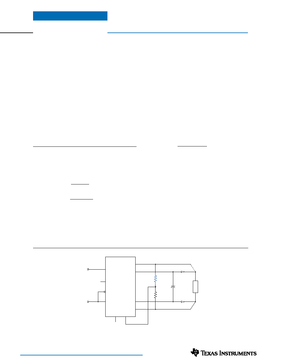
Positive Output Enable (Negative Inhibit)
To configure the converter for a positive enable function,
connect EN2 to -V
in
, and apply the system On/Off control
signal to EN1. In this configuration, applying less than
0.8V (with respect to -V
in
) to EN1 disables the converter
outputs. Figure 2-1 is an example of this implemention.
DC/DC
Module
EN 1
EN 2
≠Vin
≠V
IN
1 =Outputs Off
1
2
3
BSS138
DC/DC
Module
EN 1
EN 2
≠Vin
≠V
IN
1 =Outputs On
1
2
3
BSS138
Figure 2-2; Negative Enable Configuration
Figure 2-1; Positive Enable Configuration
Negative Output Enable (Positive Inhibit)
To configure the converter for a negative enable function,
EN1 is left open circuit, and the system On/Off control
signal is applied to EN2. Applying less than 0.8V (with
respect to -V
in
) to EN2, enables the converter outputs. An
example of this configuration is provided in Figure 2-2.
Note: The converter will only produce an output voltage if a
valid input voltage is applied to ±V
in
.
Vo (2V/Div)
V
EN1
(5V/Div)
HORIZ SCALE: 5ms/DIV
Delay Time
Figure 2-3; PT3401 Enable Turn-On

For technical support and more information, see inside back cover or visit www.ti.com
Application Notes
Using the Power-Up Sequencing Feature of the
PT3400 Series of DC/DC Converters
Introduction
Power-up sequencing is a term used to describe the
order and timing that supply voltages power up in a
multi-voltage power supply system. Multi-voltage power
supply architectures are a common place requirement in
electronic circuits that employ high-performance mi-
croprocessors or digital signal processors (DSPs). These
circuits require a tightly regulated low-voltage supply
for the processor core, and a higher voltage to power
the processor's system interface or I/O circuitry. Power-
up sequencing is often required between two such voltages
in order to manage the voltage differential during the brief
period of power-up. This reduces stress and improves the
long term reliability of the dual-voltage devices and their
associated circuitry. The most popular solution is termed
"Simultaneous Startup," whereby the two affected voltages
both start at the same time and then rise at the same rate.
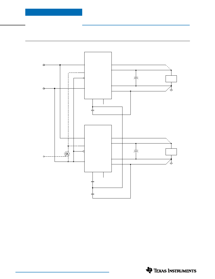
Configuration for Power-up Sequencing
The PT3400 series converters have a feature that allows
individual modules to be easily configured for simulta-
neous startup. Using the SEQ control (pin 5), two PT3400
modules are simply interconnected with just a few passive
components. This eliminates much of the application
circuitry that would otherwise be required for this type of
setup. The schematic is given in Figure 4-1. The setup is
relatively simple but varies slightly with the combination
of output voltages being sequenced. Capacitor C
3
(5)
is only
required when the modules selected are a mix between
a high-voltage module (3.3V through 1.8V), and a low-
voltage module (
1.5V). For all other configurations
C
3
is replaced by a wire link. For clarification Table 4-1
indicates which modules are a high voltage type (Type A),
and which are a low voltage type (Type B). Table 4-2
provides guidance as to the one combination that requires
the capacitor C
3
. Examples of waveforms obtained from a
sequenced start-up between two PT3400 series modules
are provided in Figure 4-2, Figure 4-3, and Figure 4-4.
In each case the voltage difference during the synchronized
portion of the power up sequence is typically within 0.4V.
Both the timing and tracking of output voltages during
the power-up sequence will vary slightly with input voltage,
temperature, and with differences in the output capaci-
tance and load current between the two converter modules.
This power-up sequencing solution may not be suitable
for every application. To ensure compatibility the appli-
cation should be tested against all variances. For additional
support please contact a Plug-in Power applications
specialist.
PT3400 Series
Table 4-1; PT3400 Module Type Identification
PART No.
VOUT
TYPE A
TYPE B
PT3401
(3.3V)
◊
PT3402
(2.5V)
◊
PT3403
(1.8V)
◊
PT3404
(1.5V)
◊
PT3405
(1.4V)
◊
PT3406
(1.2V)
◊
PT3407
(1.0V)
◊
Table 4-2; Value of C
3
in Sequencing Setup
MODULE #1 MODULE #2
C
3
COMMENTS
A
A
Wire link
Waveforms given in Figure 4-2
B
B
Wire link
Waveforms given in Figure 4-3
A
B
0.1µF
(5)
Waveforms given in Figure 4-4
Notes
1. The two converters configured for sequenced power up
must be located close together on the same printed circuit
board.
2. When configured for power-up sequencing, a minimum
of 1,000µF output capacitance is recommended at the
output of each converter.
3. The best results are obtained if a load of 1A or greater is
present at both converter outputs.
4. The capacitors, C
1
and C
2
, should each be placed close to
their associated converter, Module #1, and Module #2
respectively. Combining C
1
and C
2
to a single capacitor of
equivalent value is not recommended.
5. The capacitor C
3
is only required whenever a Type A and
Type B converter are connected together for sequenced
power-up. In this event C
3
should always be connected to
the SEQ control (pin 5) of the Type B module, or the
converter with the lowest output voltage. For all other
converter configurations C
3
is not required, and is
replaced by a copper trace or wire link.
6. The capacitors selected for C
1
, C
2
, & C
3
should be of
good quality and have stable characteristics. Capacitors
with an X7R dielectric, and 5% tolerance are
recommended.
7. The enable controls, EN1 & EN2, are optional for a
sequenced pair of converters. If an enable signal is desired,
EN1 or EN2 of both converters units must be controlled
from a single transistor.
Application Notes
For technical support and more information, see inside back cover or visit www.ti.com
Figure 4-1; Configuration for Power-Up Sequencing
Remote Sense (≠)
Remote Sense (+)
+V
IN
≠V
IN
C
OUT
1,000µF
+
Remote Sense (≠)
Remote Sense (+)
C
OUT
1,000µF
+
1 =Inhibit
Q
1
BSS138
(Note 8)
C
2
0.1µF
(Note 4)
Module #1
(Highest V
o
)
1
2
11≠13
8≠10
14
7
3
4
≠V
IN
+V
IN
EN 1
EN 2
SEQ
V
o
Adj
6
5
+V
OUT
≠V
OUT
+Sense
≠Sense
C
1
0.1µF
(Note 4)
Module #2
(Lowest V
o
)
1
2
11≠13
8≠10
14
7
3
4
≠V
IN
+V
IN
EN 1
EN 2
SEQ
V
o
Adj
6
5
+V
OUT
≠V
OUT
+Sense
≠Sense
C
3
( N o t e 5 &
T a b l e 4 - 2 )
LOAD
Vo
1
LOAD
Vo
2
For sequencing configurations, a 1,000µF
electrolytic capacitor is recommended at
the output of each converter. See Note 2.
PT3400 Series
For technical support and more information, see inside back cover or visit www.ti.com
Application Notes
Vo1 (1V/Div)
Vo2 (1V/Div)
HORIZ SCALE: 5ms/Div
Vo1 (1V/Div)
Vo2 (1V/Div)
HORIZ SCALE: 5ms/Div
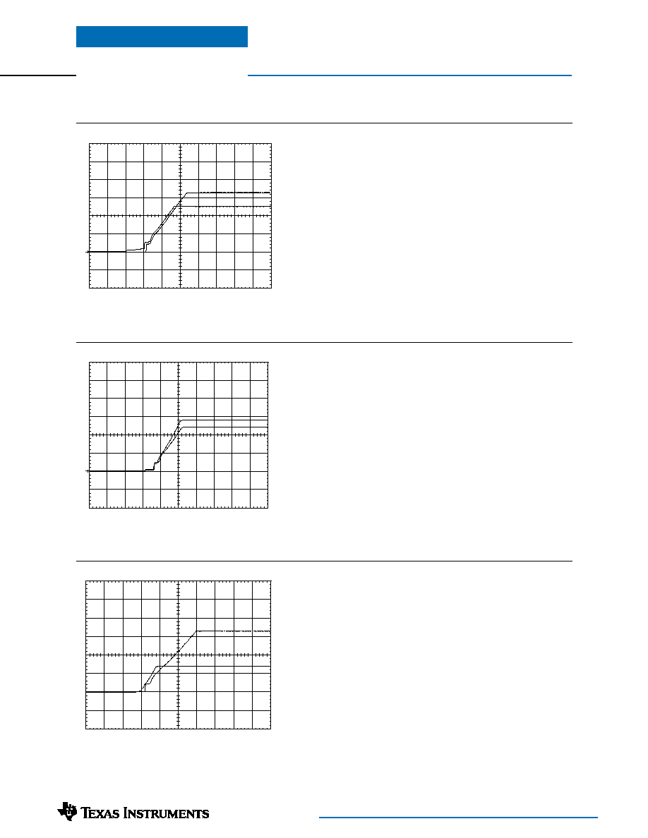
Figure 4-2; Power-Up Sequence Example with Two Type `B' Modules
Figure 4-3; Power-Up Sequence Example with Two Type `A' Modules
Figure 4-4; Power-Up Sequence Example Using Type `A' & `B' Modules
The adjacent plot shows an example of power-
up sequencing between two Type `A' modules.
In this example the PT3401 (3.3V) and PT3402
(2.5V) are featured. Each converter had a con-
stant current load of 5A applied to its respective
output.
The adjacent plot shows an example of power-
up sequencing between a Type `A' and a Type
`B' module. In this example the PT3401 (3.3V)
and PT3405 (1.4V) are featured. Each converter
had a constant current load of 5A applied to its
respective output.
The adjacent plot shows an example of power-
up sequencing between two Type `B' modules.
In this example the PT3405 (1.4V) and PT3406
(1.2V) are featured. Each converter had a con-
stant current load of 5A applied to its respective
output.
Vo1 (0.5V/Div)
Vo2 (0.5V/Div)
HORIZ SCALE: 5ms/Div
PT3400 Series

IMPORTANT NOTICE
Texas Instruments Incorporated and its subsidiaries (TI) reserve the right to make corrections, modifications,
enhancements, improvements, and other changes to its products and services at any time and to discontinue
any product or service without notice. Customers should obtain the latest relevant information before placing
orders and should verify that such information is current and complete. All products are sold subject to TI's terms
and conditions of sale supplied at the time of order acknowledgment.
TI warrants performance of its hardware products to the specifications applicable at the time of sale in
accordance with TI's standard warranty. Testing and other quality control techniques are used to the extent TI
deems necessary to support this warranty. Except where mandated by government requirements, testing of all
parameters of each product is not necessarily performed.
TI assumes no liability for applications assistance or customer product design. Customers are responsible for
their products and applications using TI components. To minimize the risks associated with customer products
and applications, customers should provide adequate design and operating safeguards.
TI does not warrant or represent that any license, either express or implied, is granted under any TI patent right,
copyright, mask work right, or other TI intellectual property right relating to any combination, machine, or process
in which TI products or services are used. Information published by TI regarding third≠party products or services
does not constitute a license from TI to use such products or services or a warranty or endorsement thereof.
Use of such information may require a license from a third party under the patents or other intellectual property
of the third party, or a license from TI under the patents or other intellectual property of TI.
Reproduction of information in TI data books or data sheets is permissible only if reproduction is without
alteration and is accompanied by all associated warranties, conditions, limitations, and notices. Reproduction
of this information with alteration is an unfair and deceptive business practice. TI is not responsible or liable for
such altered documentation.
Resale of TI products or services with statements different from or beyond the parameters stated by TI for that
product or service voids all express and any implied warranties for the associated TI product or service and
is an unfair and deceptive business practice. TI is not responsible or liable for any such statements.
Mailing Address:
Texas Instruments
Post Office Box 655303
Dallas, Texas 75265
Copyright
2002, Texas Instruments Incorporated