 | –≠–ª–µ–∫—Ç—Ä–æ–Ω–Ω—ã–π –∫–æ–º–ø–æ–Ω–µ–Ω—Ç: PT5500 | –°–∫–∞—á–∞—Ç—å:  PDF PDF  ZIP ZIP |

For technical support and more information, see inside back cover or visit www.ti.com
PT5500 Series
3-A 5-V/3.3-V Input Adjustable
Integrated Switching Regulator
SLTS132A
(Revised 10/5/2001)
Standard Application
C1 = Optional 1µF ceramic
C2 = Required 100µF (See Notes)
Ordering Information
PT5501
® =3.3 Volts
PT5502
® =2.5 Volts
PT5503
® =2.0 Volts
PT5504
® =1.8 Volts
PT5505
® =1.5 Volts
PT5506
® =1.2 Volts
PT5507
® =1.0 Volts
Pin
Function
1
Inhibit *
2
V
in
3
GND
4
V
o
5
V
o
Adjust
Features
∑
Single-Device: 5V/3.3V Input
∑
DSP Compatible
∑
90% Efficiency
∑
Small Footprint
∑
Space-Saving package
∑
Adjustable Output Voltage
∑
Output Inhibit Function
∑
Short Circuit Protection
∑
Solderable Copper Case
Pin-Out Information
C
1
C
2
+ V
O
C O M
C O M
+ V
IN
+
P T 5 5 0 0
2
3
5
4
1
I N H
V
O
A D J
* For Inhibit pin:
Open = output enabled
Ground = output disabled
Description
The PT5500 ExcaliburTM power modules
are a series of high-performance Integrated
Switching Regulators (ISRs). Rated 3A,
these modules operate from input voltages as
low as 3.1V to provide a local step-down
power source. They are an ideal compliment
to the industry's latest high-performance DSPs
and microprocessors. The series includes
output voltage options as low as 1.0VDC.
The PT5500 series is packaged in a 5-pin
thermally efficient copper case. The case is
solderable, has a small footprint, and can
accommodate both through-hole and surface
mount pin configurations.
The product features external output
voltage adjustment, an inhibit function, and
short circuit protection. A 100µF capacitor
is required for proper operation.
PT Series Suffix
(PT1234
x
)
Case/Pin
Order
Package
Configuration
Suffix
Code
Vertical
N
(EFK)
Horizontal
A
(EFL)
SMD
C
(EFM)
(Reference the applicable package code draw-
ing for the dimensions and PC board layout)
For technical support and more information, see inside back cover or visit www.ti.com
PT5500 Series
3-A 5-V/3.3-V Input Adjustable
Integrated Switching Regulator
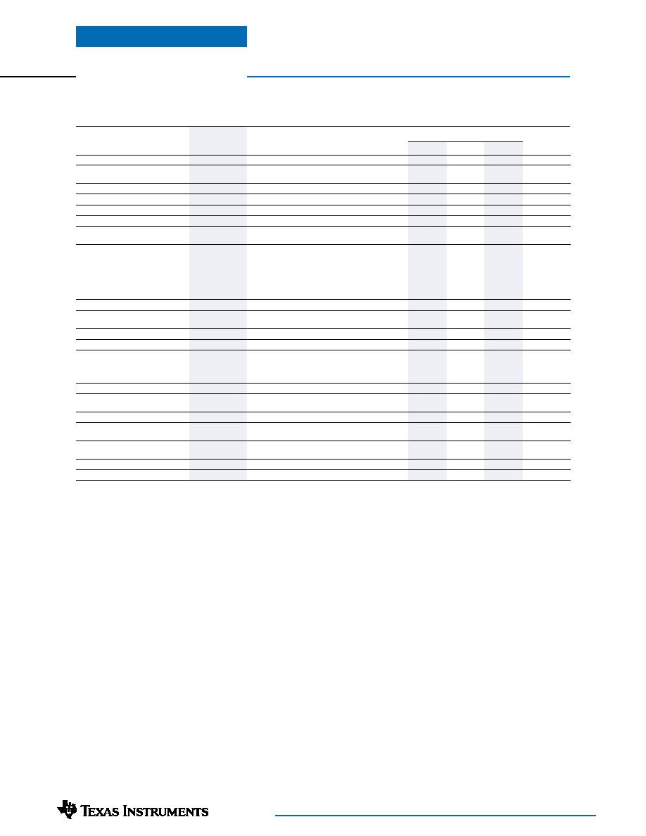
Specifications
(Unless otherwise stated, T
a
=25∞C, V
in
=5V, C
out
=100µF, and I
o
=I
o
max)
PT5500 SERIES
Characteristics
Symbols
Conditions
Min
Typ
Max
Units
Output Current
I
o
Over V
in
range
0.1
(1)
--
3.0
A
Input Voltage Range
V
in
Over I
o
range
V
o
=3.3V4.5
--
5.5
V
V
o
2.5V3.1
5.5
Set-Point Voltage Tolerance
V
o
tol
--
--
±2
%V
o
Temperature Variation
Reg
temp
≠40∞C <T
a
< +85∞C
--
±0.5
--
%V
o
Line Regulation
Reg
line
Over V
in
range
--
--
±6
mV
Load Regulation
Reg
load
Over I
o
range
--
--
±10
mV
Total Output Variation
Reg
tot
Includes set-point, line, load,
--
--
±3
%V
o
≠40∞C
T
a
+85∞C
Efficiency
PT5501
--
90
--
PT5502
--
87
--
PT5503
--
85
--
PT5504
--
83
--
%
PT5505
--
81
--
PT5506
--
79
--
PT5507
--
76
--
V
o
Ripple (pk-pk)
V
r
20MHz bandwidth
--
25
45
mV
Transient Response
t
tr
1A/µs load step from 50% to 100% I
o
max
--
50
--
µSec
V
tr
V
o
over/undershoot
--
50
100
mV
Current Limit
I
lim
--
5
--
A
Switching Frequency
o
Over V
in
and I
o
ranges
--
350
(2)
--
kHz
Inhibit Control (pin1)
Input High Voltage
V
IH
Referenced to GND (pin3)
V
in
≠0.5
--
Open
(3)
V
Input Low Voltage
V
IL
≠0.2
--
0.5
Input Low Current
I
IL
Pin 1 to GND
--
≠0.5
--
mA
External Capacitance
C
out
100
(4)
--
--
µF
Absolute Maximum
T
a
Over V
in
range
≠40
(5)
--
+85
(6)
∞C
Operating Temperature Range
Storage Temperature
T
s
--
-40
--
+125
∞C
Mechanical Shock
Per Mil-STD-883D, Method 2002.3 , 1 msec,
--
500
--
G's
Half Sine, mounted to a fixture
Mechanical Vibration
Per Mil-STD-883D, Method 2007.2,
20-2000 Hz, Soldered in a PC board
--
15
(7)
--
G's
Weight
--
--
--
6.5
--
grams
Flammability
--
Materials meet UL 94V-0
Notes: (1) The ISR will operate down to no load with reduced specifications.
(2) This is a typical value only. The switching frequency will vary with input voltage.
(3) The Inhibit control (pin 1) has an internal pull-up, and if left open-circuit the module will operate when input power is applied. A small low-leakage
(<100nA) MOSFET is recommended to control this input. Ensure an On/Off transition time of
10µs. See application notes for more information.
(4) The PT5500 Series requires a 100µF electrolytic or tantalum output capacitor for proper operation in all applications.
(5) For operation below 0∞C, the output capacitor C
2
must have stable characteristics. Use either a low ESR tantalum or OsconÆ capacitor.
(6) See SOA curves or consult factory for the appropriate derating.
(7) The case pins on the through-hole package types (suffixes N & A) must be soldered. For more information see the applicable package outline drawing.

For technical support and more information, see inside back cover or visit www.ti.com
Note A:
Characteristic data has been developed from actual products tested at 25∞C. This data is considered typical data for the ISR.
Note B:
SOA curves represent operating conditions at which internal components are at or below manufacturer's maximum rated operating temperatures.
Ripple vs Output Current
Efficiency vs Output Current
Efficiency vs Output Current
Ripple vs Output Current
Power Dissipation vs Output Current
Power Dissipation vs Output Current
Safe Operating Area; V
in
=5.0V
(See Note B)
Performance Data; V
in
=5.0V
(See Note A)
Performance Data; V
in
=3.3V
(See Note A)
Safe Operating Area; V
in
=3.3V
(See Note B)
20.0
30.0
40.0
50.0
60.0
70.0
80.0
90.0
0.0
0.5
1.0
1.5
2.0
2.5
3.0
Iout (A)
Ambient Temperature (∞C)
200LFM
120LFM
60LFM
Nat conv
Airflow
30.0
40.0
50.0
60.0
70.0
80.0
90.0
0.0
0.5
1.0
1.5
2.0
2.5
3.0
Iout (A)
Ambient Temperature (
∞
C)
200LFM
120LFM
60LFM
Nat conv
Airflow
PT5500 Series
3-A 5-V/3.3-V Input Adjustable
Integrated Switching Regulator
40
50
60
70
80
90
100
0
0.5
1
1.5
2
2.5
3
Iout (A)
Efficiency - %
PT5501
PT5502
PT5504
PT5505
0
10
20
30
40
0
0.5
1
1.5
2
2.5
3
Iout (A)
Ripple - mV
PT5505
PT5504
PT5502
PT5501
50
60
70
80
90
100
0
0.5
1
1.5
2
2.5
3
Iout (A)
Efficiency - %
PT5502
PT5504
PT5505
0
10
20
30
40
0
0.5
1
1.5
2
2.5
3
Iout (A)
Ripple - mV
PT5505
PT5504
PT5502
0
0.25
0.5
0.75
1
1.25
0
0.5
1
1.5
2
2.5
3
Iout (A)
Pd - Watts
PT5502
PT5504
PT5505
PT5501
0
0.25
0.5
0.75
1
1.25
0
0.5
1
1.5
2
2.5
3
Iout (A)
Pd - Watts
PT5505
PT5504
PT5502
Typical Characteristics

Application Notes
For technical support and more information, see inside back cover or visit www.ti.com
PT5500/5520 Series
Adjusting the Output Voltage of the PT5500/20
Series of Excalibur
Step-Down ISRs
The output voltage of both the PT5500 and PT5520
series ISRs may be adjusted higher or lower than the
factory trimmed pre-set voltage with the addition of a
single external resistor. Table 1 accordingly gives the
allowable adjustment range for each model for either
series as V
a
(min) and V
a
(max).
Adjust Up:
An increase in the output voltage is obtained by
adding a resistor R
2
, between pin 5 (V
o
adj) and pin 3 (GND).
Adjust Down:
Add a resistor
(R
1
)
, between pin 5 (V
o
adj) and
pin 4 (V
out
).
Figure 1
The values of
(R
1
)
[adjust down], and R
2
[adjust up], can
also be calculated using the following formulas. Refer to
Figure 1 and Table 2 for both the placement and value of the
required resistor; either
(R
1
)
or R
2
as appropriate.
(R
1
)
=
R
o
(V
a
≠ 0.9)
≠ R
s
k
V
o
≠ V
a
R
2
=
0.9 R
o
≠ R
s
k
V
a
≠ V
o
Where:
V
o
= Original output voltage
V
a
= Adjusted output voltage
R
o
= The resistance value from Table 1
R
s
= The series resistance from Table 1
Table 1
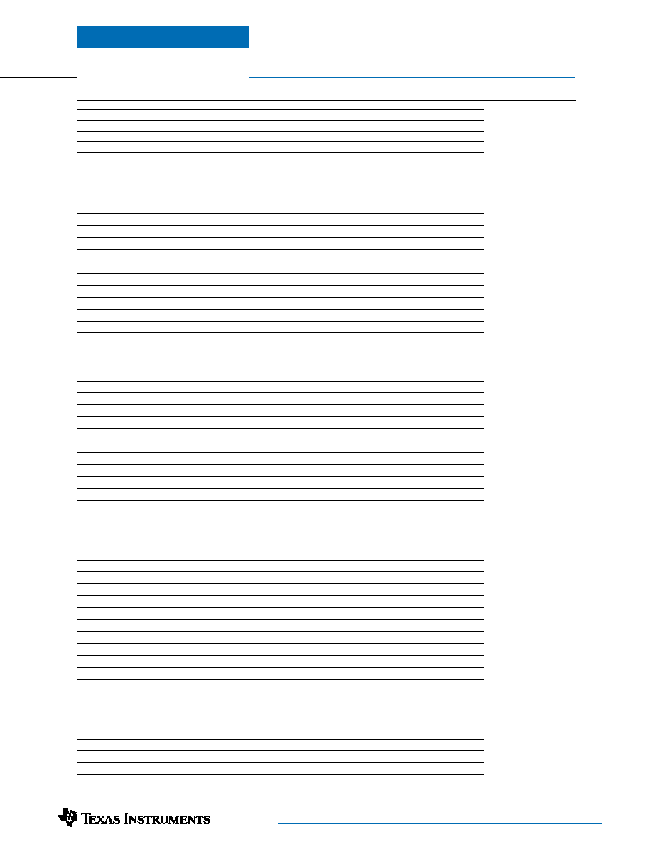
ISR ADJUSTMENT RANGE AND FORMULA PARAMETERS
3.0 Adc Rated
PT5501
PT5502
PT5503
PT5504
PT5505
PT5506
PT5507
1.5 Adc Rated
PT5521
PT5522
PT5523
PT5524
PT5525
PT5526
PT5527
Vo (nom)
3.3
2.5
2.0
1.8
1.5
1.2
1.0
Va (min)
2.88
1.97
1.64
1.5
1.3
1.08
0.97
Va (max)
3.5
2.95
2.45
2.25
1.95
1.65
1.45
Ro (k
)
10.0
10.0
10.0
10.0
10.0
10.0
10.2
Rs (k
)
49.9
20.0
20.0
20.0
20.0
20.0
20.0
R 2
A d j u s t U p
C 1
1
µ
F C e r a m i c
(Optional)
C 2
1 0 0
µ
F
(Req'd)
+ V
O
C O M
C O M
+ V
IN
+
( R 1 )
A d j D o w n
P T 5 5 0 0
2
3
5
4
V in
V o
Vo(adj)
G N D
Notes:
1. Use only a single 1% resistor in either the
(R
1
)
or R
2
location. Place the resistor as close to the ISR as possible.
2. Never connect capacitors from V
o
adj to either GND or
V
out
. Any capacitance added to the V
o
adjust pin will
affect the stability of the ISR.
3. For each model, adjustments to the output voltage may
place additional limits on the minimum input voltage.
The revised minimum input voltage must comply with the
following requirement.
V
in
(min) = (V
a
+ 0.5)V or as specified in the data sheet,
whichever is greater.
For technical support and more information, see inside back cover or visit www.ti.com
Application Notes
continued
ISR ADJUSTMENT RESISTOR VALUES
3.0 Adc Rated
PT5501
PT5502
PT5503
PT5504
PT5505
PT5506
PT5507
1.5 Adc Rated
PT5521
PT5522
PT5523
PT5524
PT5525
PT5526
PT5527
V
o
(nom)
3.3
2.5
2.0
1.8
1.5
1.2
1.0
V
a
(req.d)
0.97
(0.0)k
1.0
1.05
164.0k
1.1
(0.0)k
72.8k
1.15
(30.0)k
41.2k
1.2
25.9k
1.25
160.0k
16.7k
1.3
(0.0)k
70.0k
10.6k
1.35
(10.0)k
40.0k
6.2k
1.4
(30.0)k
25.0k
3.0k
1.45
(90.0)k
16.0k
0.4k
1.5
(0.0)k
10.0k
1.55
(6.0)k
160.0k
5.7k
1.6
(15.0)k
70.0k
2.5k
1.65
(1.4)k
(30.0)k
40.0k
0.0k
1.7
(6.7)k
(60.0)k
25.0k
1.75
(14.0)k
(150.0)k
16.0k
1.8
(25.0)k
10.0k
1.85
(43.3)k
160.0k
5.7k
1.9
(80.0)k
70.0k
2.5k
1.95
(190.0)k
40.0k
0.0k
2.0
(2.0)k
25.0k
2.05
(5.6)k
160.0k
16.0k
2.1
(10.0)k
70.0k
10.0k
2.15
(15.7)k
0.0k
5.7k
2.2
(23.3)k
25.0k
2.5k
2.25
(34.0)k
16.0k
0.0k
2.3
(50.0)k
10.0k
2.35
(76.7)k
5.7k
2.4
(130.0)k
2.5k
2.45
(284.0)k
0.0k
2.5
2.55
160.0k
2.6
70.0k
2.65
40.0k
2.7
25.0k
2.75
16.0k
2.8
10.0k
2.85
5.7k
2.9
(0.0k
2.5k
2.95
(8.5)k
0.0k
3.0
(20.1)k
3.05
(36.1)k
3.1
(60.1)k
3.15
(100.0)k
3.2
(180.0)k
3.25
(420.0)k
3.3
3.35
130.0k
3.4
40.1k
3.45
10.1k
3.48
0.0k
R1 =
(Blue)
R2 = Black
Table 2
PT5500/5520 Series