SN54AHCT16373, SN74AHCT16373
16-BIT TRANSPARENT D-TYPE LATCHES
WITH 3-STATE OUTPUTS
SCLS336H ≠ MARCH 1996 ≠ REVISED JANUARY 2000
1
POST OFFICE BOX 655303
∑
DALLAS, TEXAS 75265
D
Members of the Texas Instruments
Widebus
TM
Family
D
EPIC
TM
(Enhanced-Performance Implanted
CMOS) Process
D
Inputs Are TTL-Voltage Compatible
D
Distributed V
CC
and GND Pins Minimize
High-Speed Switching Noise
D
Flow-Through Architecture Optimizes PCB
Layout
D
Latch-Up Performance Exceeds 250 mA Per
JESD 17
D
ESD Protection Exceeds 2000 V Per
MIL-STD-883, Method 3015; Exceeds 200 V
Using Machine Model (C = 200 pF, R = 0)
D
Package Options Include Plastic Shrink
Small-Outline (DL), Thin Shrink
Small-Outline (DGG), and Thin Very
Small-Outline (DGV) Packages and 380-mil
Fine-Pitch Ceramic Flat (WD) Package
Using 25-mil Center-to-Center Spacings
description
The 'AHCT16373 devices are 16-bit transparent
D-type latches with 3-state outputs designed
specifically for driving highly capacitive or
relatively low-impedance loads. They are
particularly suitable for implementing buffer
registers, I/O ports, bidirectional bus drivers, and
working registers.
These devices can be used as two 8-bit latches or one 16-bit latch. When the latch-enable (LE) input is high,
the Q outputs follow the data (D) inputs. When LE is taken low, the Q outputs are latched at the levels set up
at the D inputs.
A buffered output-enable (OE) input can be used to place the eight outputs in either a normal logic state (high
or low logic levels) or the high-impedance state. In the high-impedance state, the outputs neither load nor drive
the bus lines significantly. The high-impedance state and the increased drive provide the capability to drive bus
lines without need for interface or pullup components.
OE does not affect internal operations of the latch. Old data can be retained or new data can be entered while
the outputs are in the high-impedance state.
To ensure the high-impedance state during power up or power down, OE should be tied to V
CC
through a pullup
resistor; the minimum value of the resistor is determined by the current-sinking capability of the driver.
The SN54AHCT16373 is characterized for operation over the full military temperature range of ≠55
∞
C to 125
∞
C.
The SN74AHCT16373 is characterized for operation from ≠40
∞
C to 85
∞
C.
Copyright
©
2000, Texas Instruments Incorporated
UNLESS OTHERWISE NOTED this document contains PRODUCTION
DATA information current as of publication date. Products conform to
specifications per the terms of Texas Instruments standard warranty.
Production processing does not necessarily include testing of all
parameters.
Please be aware that an important notice concerning availability, standard warranty, and use in critical applications of
Texas Instruments semiconductor products and disclaimers thereto appears at the end of this data sheet.
EPIC and Widebus are trademarks of Texas Instruments Incorporated.
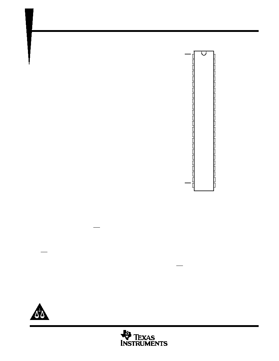
SN54AHCT16373 . . . WD PACKAGE
SN74AHCT16373 . . . DGG, DGV, OR DL PACKAGE
(TOP VIEW)
1
2
3
4
5
6
7
8
9
10
11
12
13
14
15
16
17
18
19
20
21
22
23
24
48
47
46
45
44
43
42
41
40
39
38
37
36
35
34
33
32
31
30
29
28
27
26
25
1OE
1Q1
1Q2
GND
1Q3
1Q4
V
CC
1Q5
1Q6
GND
1Q7
1Q8
2Q1
2Q2
GND
2Q3
2Q4
V
CC
2Q5
2Q6
GND
2Q7
2Q8
2OE
1LE
1D1
1D2
GND
1D3
1D4
V
CC
1D5
1D6
GND
1D7
1D8
2D1
2D2
GND
2D3
2D4
V
CC
2D5
2D6
GND
2D7
2D8
2LE
SN54AHCT16373, SN74AHCT16373
16-BIT TRANSPARENT D-TYPE LATCHES
WITH 3-STATE OUTPUTS
SCLS336H ≠ MARCH 1996 ≠ REVISED JANUARY 2000
2
POST OFFICE BOX 655303
∑
DALLAS, TEXAS 75265
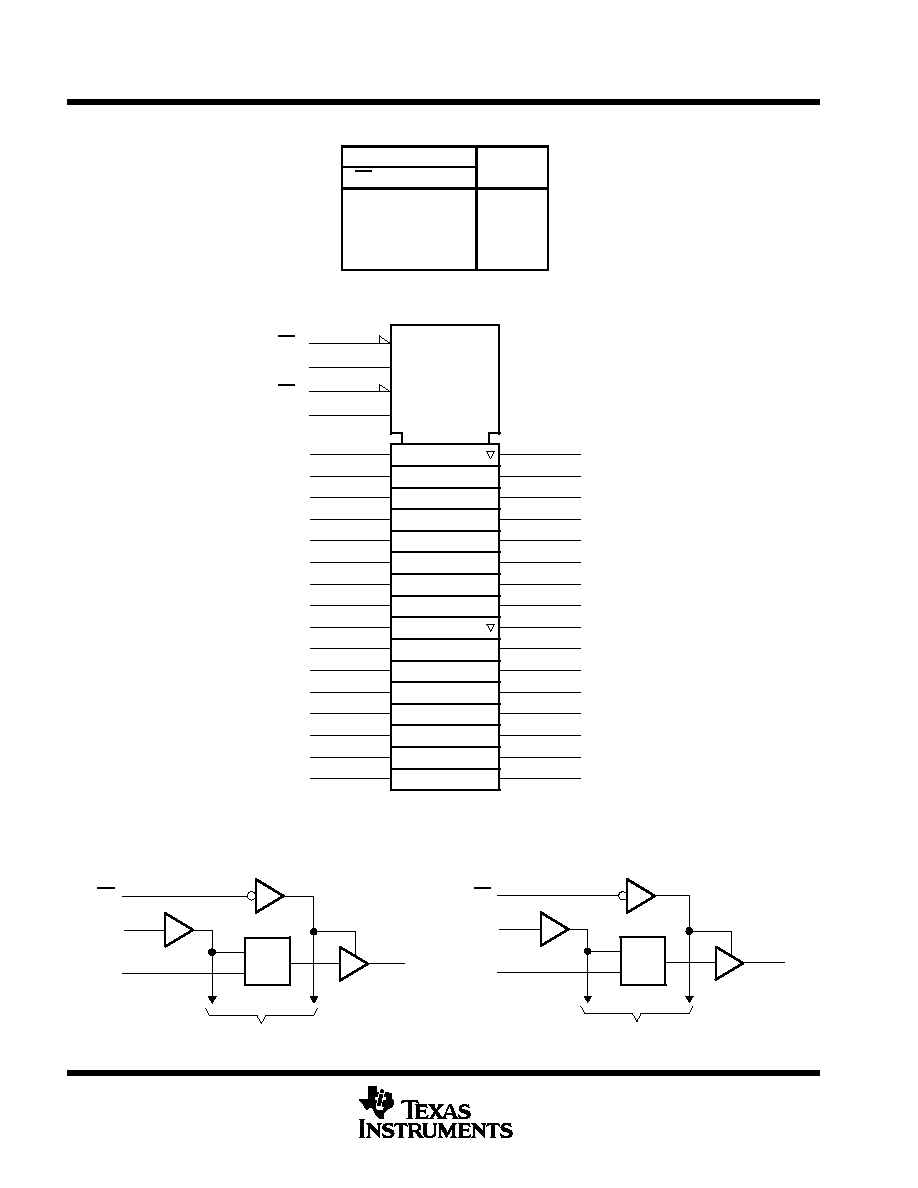
FUNCTION TABLE
(each 8-bit latch)
INPUTS
OUTPUT
OE
LE
D
Q
L
H
H
H
L
H
L
L
L
L
X
Q0
H
X
X
Z
logic symbol
This symbol is in accordance with ANSI/IEEE Std 91-1984 and IEC Publication 617-12.
1OE
2OE
1EN
1
C3
48
1LE
3D
47
1D1
46
1D2
44
1D3
43
1D4
1Q1
2
1Q2
3
1Q3
5
1Q4
6
41
1D5
40
1D6
38
1D7
37
1D8
1Q5
8
1Q6
9
1Q7
11
1Q8
12
4D
36
2D1
35
2D2
33
2D3
32
2D4
2Q1
13
2Q2
14
2Q3
16
2Q4
17
30
2D5
29
2D6
27
2D7
26
2D8
2Q5
19
2Q6
20
2Q7
22
2Q8
23
2EN
24
C4
25
2LE
1
2
logic diagram (positive logic)
1OE
1LE
1D1
To Seven Other Channels
1Q1
2OE
2LE
2D1
2Q1
To Seven Other Channels
1
48
47
24
25
36
C1
1D
13
2
C1
1D
SN54AHCT16373, SN74AHCT16373
16-BIT TRANSPARENT D-TYPE LATCHES
WITH 3-STATE OUTPUTS
SCLS336H ≠ MARCH 1996 ≠ REVISED JANUARY 2000
3
POST OFFICE BOX 655303
∑
DALLAS, TEXAS 75265
absolute maximum ratings over operating free-air temperature range (unless otherwise noted)
Supply voltage range, V
CC
≠0.5 V to 7 V
. . . . . . . . . . . . . . . . . . . . . . . . . . . . . . . . . . . . . . . . . . . . . . . . . . . . . . . . . .
Input voltage range, V
I
(see Note 1)
≠0.5 V to 7 V
. . . . . . . . . . . . . . . . . . . . . . . . . . . . . . . . . . . . . . . . . . . . . . . . . .
Output voltage range, V
O
(see Note 1)
≠0.5 V to V
CC
+ 0.5 V
. . . . . . . . . . . . . . . . . . . . . . . . . . . . . . . . . . . . . . . .
Input clamp current, I
IK
(V
I
< 0)
≠20 mA
. . . . . . . . . . . . . . . . . . . . . . . . . . . . . . . . . . . . . . . . . . . . . . . . . . . . . . . . . . .
Output clamp current, I
OK
(V
O
< 0 or V
O
> V
CC
)
±
20 mA
. . . . . . . . . . . . . . . . . . . . . . . . . . . . . . . . . . . . . . . . . . . .
Continuous output current, I
O
(V
O
= 0 to V
CC
)
±
25 mA
. . . . . . . . . . . . . . . . . . . . . . . . . . . . . . . . . . . . . . . . . . . . . .
Continuous current through each V
CC
or GND
±
75 mA
. . . . . . . . . . . . . . . . . . . . . . . . . . . . . . . . . . . . . . . . . . . . . .
Package thermal impedance,
JA
(see Note 2): DGG package
70
∞
C/W
. . . . . . . . . . . . . . . . . . . . . . . . . . . . . . .
DGV package
58
∞
C/W
. . . . . . . . . . . . . . . . . . . . . . . . . . . . . . . .
DL package
63
∞
C/W
. . . . . . . . . . . . . . . . . . . . . . . . . . . . . . . . .
Storage temperature range, T
stg
≠65
∞
C to 150
∞
C
. . . . . . . . . . . . . . . . . . . . . . . . . . . . . . . . . . . . . . . . . . . . . . . . . . .
Stresses beyond those listed under "absolute maximum ratings" may cause permanent damage to the device. These are stress ratings only, and
functional operation of the device at these or any other conditions beyond those indicated under "recommended operating conditions" is not
implied. Exposure to absolute-maximum-rated conditions for extended periods may affect device reliability.
NOTES:
1. The input and output voltage ratings may be exceeded if the input and output current ratings are observed.
2. The package thermal impedance is calculated in accordance with JESD 51.
recommended operating conditions (see Note 3)
SN54AHCT16373
SN74AHCT16373
UNIT
MIN
MAX
MIN
MAX
UNIT
VCC
Supply voltage
4.5
5.5
4.5
5.5
V
VIH
High-level input voltage
2
2
V
VIL
Low-level input voltage
0.8
0.8
V
VI
Input voltage
0
5.5
0
5.5
V
VO
Output voltage
0
VCC
0
VCC
V
IOH
High-level output current
≠8
≠8
mA
IOL
Low-level output current
8
8
mA
t/
v
Input transition rise or fall rate
20
20
ns/V
TA
Operating free-air temperature
≠55
125
≠40
85
∞
C
NOTE 3: All unused inputs of the device must be held at VCC or GND to ensure proper device operation. Refer to the TI application report,
Implications of Slow or Floating CMOS Inputs, literature number SCBA004.
PRODUCT PREVIEW information concerns products in the formative or
design phase of development. Characteristic data and other
specifications are design goals. Texas Instruments reserves the right to
change or discontinue these products without notice.
SN54AHCT16373, SN74AHCT16373
16-BIT TRANSPARENT D-TYPE LATCHES
WITH 3-STATE OUTPUTS
SCLS336H ≠ MARCH 1996 ≠ REVISED JANUARY 2000
4
POST OFFICE BOX 655303
∑
DALLAS, TEXAS 75265
electrical characteristics over recommended operating free-air temperature range (unless
otherwise noted)
PARAMETER
TEST CONDITIONS
VCC
TA = 25
∞
C
SN54AHCT16373
SN74AHCT16373
UNIT
PARAMETER
TEST CONDITIONS
VCC
MIN
TYP
MAX
MIN
MAX
MIN
MAX
UNIT
VOH
IOH = ≠50
m
A
4 5 V
4.4
4.5
4.4
4.4
V
VOH
IOH = ≠8 mA
4.5 V
3.94
3.8
3.8
V
VOL
IOL = 50
m
A
4 5 V
0.1
0.1
0.1
V
VOL
IOL = 8 mA
4.5 V
0.36
0.44
0.44
V
II
VI = VCC or GND
0 V to 5.5 V
±
0.1
±
1*
±
1
m
A
IOZ
VO = VCC or GND
5.5 V
±
0.25
±
2.5
±
2.5
m
A
ICC
VI = VCC or GND,
IO = 0
5.5 V
4
40
40
m
A
ICC
One input at 3.4 V,
Other inputs at VCC or GND
5.5 V
1.35
1.5
1.5
mA
Ci
VI = VCC or GND
5 V
2.5
10
10
pF
Co
VO = VCC or GND
5 V
4.5
pF
* On products compliant to MIL-PRF-38535, this parameter is not production tested at VCC = 0 V.
This is the increase in supply current for each input at one of the specified TTL voltage levels rather than 0 V or VCC.
timing requirements over recommended operating free-air temperature range, V
CC
= 5 V
±
0.5 V
(unless otherwise noted) (see Figure 1)
TA = 25
∞
C
SN54AHCT16373
SN74AHCT16373
UNIT
MIN
MAX
MIN
MAX
MIN
MAX
UNIT
tw
Pulse duration, LE high
6.5
6.5
6.5
ns
tsu
Setup time, data before LE
1.5
1.5
1.5
ns
th
Hold time, data after LE
3.5
3.5
3.5
ns

SN54AHCT16373, SN74AHCT16373
16-BIT TRANSPARENT D-TYPE LATCHES
WITH 3-STATE OUTPUTS
SCLS336H ≠ MARCH 1996 ≠ REVISED JANUARY 2000
5
POST OFFICE BOX 655303
∑
DALLAS, TEXAS 75265
switching characteristics over recommended operating free-air temperature range,
V
CC
= 5 V
±
0.5 V (unless otherwise noted) (see Figure 1)
PARAMETER
FROM
TO
LOAD
TA = 25
∞
C
SN54AHCT16373
SN74AHCT16373
UNIT
PARAMETER
(INPUT)
(OUTPUT)
CAPACITANCE
MIN
TYP
MAX
MIN
MAX
MIN
MAX
UNIT
tPLH
D
Q
CL = 15 pF
5.1*
8.5*
1*
9.5*
1
9.5
ns
tPHL
D
Q
CL = 15 pF
5.1*
8.5*
1*
9.5*
1
9.5
ns
tPLH
LE
Q
CL = 15 pF
5*
8.5*
1*
9.5*
1
9.5
ns
tPHL
LE
Q
CL = 15 pF
5*
8.5*
1*
9.5*
1
9.5
ns
tPZH
OE
Q
CL = 15 pF
5*
9.5*
1*
10.5*
1
10.5
ns
tPZL
OE
Q
CL = 15 pF
5*
9.5*
1*
10.5*
1
10.5
ns
tPHZ
OE
Q
CL = 15 pF
6*
10.2*
1*
11*
1
11
ns
tPLZ
OE
Q
CL = 15 pF
6.8*
10.2*
1*
11*
1
11
ns
tPLH
D
Q
CL = 50 pF
5.9
9.5
1
10.5
1
10.5
ns
tPHL
D
Q
CL = 50 pF
5.9
9.5
1
10.5
1
10.5
ns
tPLH
LE
Q
CL = 50 pF
6.4
9.5
1
10.5
1
10.5
ns
tPHL
LE
Q
CL = 50 pF
5.9
9.5
1
10.5
1
10.5
ns
tPZH
OE
Q
CL = 50 pF
6
10.5
1
11.5
1
11.5
ns
tPZL
OE
Q
CL = 50 pF
6
10.5
1
11.5
1
11.5
ns
tPHZ
OE
Q
CL = 50 pF
6.8
11.2
1
12
1
12
ns
tPLZ
OE
Q
CL = 50 pF
7.8
11.2
1
12
1
12
ns
tsk(o)
CL = 50 pF
1**
1
ns
* On products compliant to MIL-PRF-38535, this parameter is not production tested.
** On products compliant to MIL-PRF-38535, this parameter does not apply.
noise characteristics, V
CC
= 5 V, C
L
= 50 pF, T
A
= 25
∞
C (see Note 4)
PARAMETER
SN74AHCT16373
UNIT
PARAMETER
MIN
TYP
MAX
UNIT
VOL(P)
Quiet output, maximum dynamic VOL
0.32
0.8
V
VOL(V)
Quiet output, minimum dynamic VOL
≠0.1
≠0.8
V
VOH(V)
Quiet output, minimum dynamic VOH
4.7
V
VIH(D)
High-level dynamic input voltage
2
V
VIL(D)
Low-level dynamic input voltage
0.8
V
NOTE 4: Characteristics are for surface-mount packages only.
operating characteristics, V
CC
= 5 V, T
A
= 25
∞
C
PARAMETER
TEST CONDITIONS
TYP
UNIT
Cpd
Power dissipation capacitance
No load,
f = 1 MHz
22
pF
PRODUCT PREVIEW information concerns products in the formative or
design phase of development. Characteristic data and other
specifications are design goals. Texas Instruments reserves the right to
change or discontinue these products without notice.