
SN54ALS240A, SN54AS240A, SN74ALS240A, SN74AS240A
OCTAL BUFFERS/DRIVERS
WITH 3-STATE OUTPUTS
SDAS214E ≠ DECEMBER 1982 ≠ REVISED AUGUST 2002
1
POST OFFICE BOX 655303
∑
DALLAS, TEXAS 75265
D
3-State Outputs Drive Bus Lines or Buffer
Memory Address Registers
D
pnp Inputs Reduce dc Loading
description/ordering information
These octal buffers/drivers are designed
specifically to improve both the performance and
density of 3-state memory address drivers, clock
drivers, and bus-oriented receivers and
transmitters. When these devices are used with
the 'ALS241, 'AS241A, 'ALS244, and 'AS244A
devices, the circuit designer has a choice of
selected combinations of inverting and
noninverting outputs, symmetrical active-low
output-enable (OE) inputs, and complementary
OE and OE inputs. These devices feature high
fan-out and improved fan-in.
The -1 version of SN74ALS240A is identical to the
standard version, except that the recommended
maximum I
OL
for the -1 version is 48 mA. There is
no -1 version of the SN54ALS240A.
ORDERING INFORMATION
TA
PACKAGE
ORDERABLE
PART NUMBER
TOP-SIDE
MARKING
SN74ALS240AN
SN74ALS240AN
PDIP ≠ N
Tube
SN74ALS240A-1N
SN74ALS240A-1N
SN74AS240AN
SN74AS240AN
Tube
SN74ALS240ADW
ALS240A
Tape and reel
SN74ALS240ADWR
ALS240A
SOIC
DW
Tube
SN74ALS240A-1DW
ALS240A 1
0
∞
C to 70
∞
C
SOIC ≠ DW
Tape and reel
SN74ALS240A-1DWR
ALS240A-1
Tube
SN74AS240ADW
AS240A
Tape and reel
SN74AS240ADWR
AS240A
SOP
NS
Tape and reel
SN74ALS240ANSR
ALS240A
SOP ≠ NS
Tape and reel
SN74ALS240A-1NSR
ALS240A-1
SSOP
DB
Tape and reel
SN74ALS240ADBR
G240A
SSOP ≠ DB
Tape and reel
SN74ALS240A-1DBR
G240A-1
Package drawings, standard packing quantities, thermal data, symbolization, and PCB design guidelines are
available at www.ti.com/sc/package.
Copyright
2002, Texas Instruments Incorporated
PRODUCTION DATA information is current as of publication date.
Products conform to specifications per the terms of Texas Instruments
standard warranty. Production processing does not necessarily include
testing of all parameters.
Please be aware that an important notice concerning availability, standard warranty, and use in critical applications of
Texas Instruments semiconductor products and disclaimers thereto appears at the end of this data sheet.
1
2
3
4
5
6
7
8
9
10
20
19
18
17
16
15
14
13
12
11
1OE
1A1
2Y4
1A2
2Y3
1A3
2Y2
1A4
2Y1
GND
V
CC
2OE
1Y1
2A4
1Y2
2A3
1Y3
2A2
1Y4
2A1
SN54ALS240A, SN54AS240A . . . J OR W PACKAGE
SN74ALS240A . . . DB, DW, N, OR NS PACKAGE
SN74AS240A . . . DW OR N PACKAGE
(TOP VIEW)
3
2
1 20 19
9 10 11 12 13
4
5
6
7
8
18
17
16
15
14
1Y1
2A4
1Y2
2A3
1Y3
1A2
2Y3
1A3
2Y2
1A4
SN54ALS240A, SN54AS240A . . . FK PACKAGE
(TOP VIEW)
2Y4
1A1
1OE
1Y4
2A2
2OE
2Y1
GND
2A1
V
CC
On products compliant to MIL-PRF-38535, all parameters are tested
unless otherwise noted. On all other products, production
processing does not necessarily include testing of all parameters.
SN54ALS240A, SN54AS240A, SN74ALS240A, SN74AS240A
OCTAL BUFFERS/DRIVERS
WITH 3-STATE OUTPUTS
SDAS214E ≠ DECEMBER 1982 ≠ REVISED AUGUST 2002
2
POST OFFICE BOX 655303
∑
DALLAS, TEXAS 75265
description/ordering information (continued)
ORDERING INFORMATION
TA
PACKAGE
ORDERABLE
PART NUMBER
TOP-SIDE
MARKING
CDIP
J
Tube
SNJ54ALS240AJ
SNJ54ALS240AJ
CDIP ≠ J
Tube
SNJ54AS240AJ
SNJ54AS240AJ
55
∞
C to 125
∞
C
CFP
W
Tube
SNJ54ALS240AW
SNJ54ALS240AW
≠55
∞
C to 125
∞
C
CFP ≠ W
Tube
SNJ54AS240AW
SNJ54AS240AW
LCCC
FK
Tube
SNJ54ALS240AFK
SNJ54ALS240AFK
LCCC ≠ FK
Tube
SNJ54AS240AFK
SNJ54AS240AFK
Package drawings, standard packing quantities, thermal data, symbolization, and PCB design guidelines are
available at www.ti.com/sc/package.
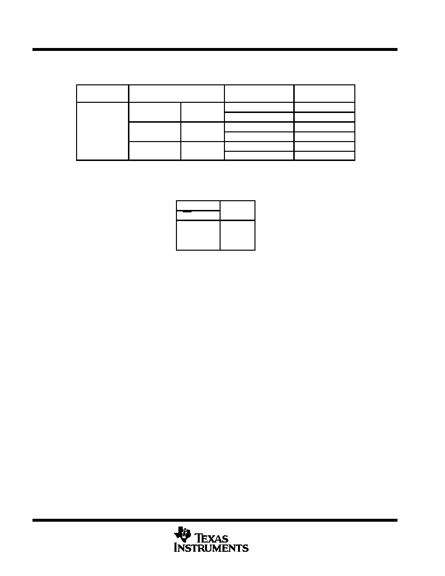
FUNCTION TABLE
(each buffer)
INPUTS
OUTPUT
OE
A
Y
L
H
L
L
L
H
H
X
Z

SN54ALS240A, SN54AS240A, SN74ALS240A, SN74AS240A
OCTAL BUFFERS/DRIVERS
WITH 3-STATE OUTPUTS
SDAS214E ≠ DECEMBER 1982 ≠ REVISED AUGUST 2002
3
POST OFFICE BOX 655303
∑
DALLAS, TEXAS 75265
logic diagram (positive logic)
1
2
4
6
8
19
11
13
15
17
3
5
7
9
12
14
16
18
1A1
1A2
1A3
1A4
1Y1
2A1
2A2
2A3
2A4
2Y1
1Y2
1Y3
1Y4
2Y2
2Y3
2Y4
1OE
2OE
absolute maximum ratings over operating free-air temperature range (unless otherwise noted)
Supply voltage, V
CC
7 V
. . . . . . . . . . . . . . . . . . . . . . . . . . . . . . . . . . . . . . . . . . . . . . . . . . . . . . . . . . . . . . . . . . . . . . . .
Input voltage, V
I
7 V
. . . . . . . . . . . . . . . . . . . . . . . . . . . . . . . . . . . . . . . . . . . . . . . . . . . . . . . . . . . . . . . . . . . . . . . . . . . .
Voltage applied to a disabled 3-state output
5.5 V
. . . . . . . . . . . . . . . . . . . . . . . . . . . . . . . . . . . . . . . . . . . . . . . . . .
Package thermal impedance,
JA
(see Note 1): DB package
70
∞
C/W
. . . . . . . . . . . . . . . . . . . . . . . . . . . . . . . . .
DW package
58
∞
C/W
. . . . . . . . . . . . . . . . . . . . . . . . . . . . . . . . .
N package
70
∞
C/W
. . . . . . . . . . . . . . . . . . . . . . . . . . . . . . . . . . .
NS package
60
∞
C/W
. . . . . . . . . . . . . . . . . . . . . . . . . . . . . . . . .
Storage temperature range, T
stg
≠ 65
∞
C to 150
∞
C
. . . . . . . . . . . . . . . . . . . . . . . . . . . . . . . . . . . . . . . . . . . . . . . . . . .
Stresses beyond those listed under "absolute maximum ratings" may cause permanent damage to the device. These are stress ratings only, and
functional operation of the device at these or any other conditions beyond those indicated under "recommended operating conditions" is not
implied. Exposure to absolute-maximum-rated conditions for extended periods may affect device reliability.
NOTE 1: The package thermal impedance is calculated in accordance with JESD 51-7.

SN54ALS240A, SN54AS240A, SN74ALS240A, SN74AS240A
OCTAL BUFFERS/DRIVERS
WITH 3-STATE OUTPUTS
SDAS214E ≠ DECEMBER 1982 ≠ REVISED AUGUST 2002
4
POST OFFICE BOX 655303
∑
DALLAS, TEXAS 75265
recommended operating conditions
MIN
NOM
MAX
UNIT
VCC
Supply voltage
4.5
5
5.5
V
VIH
High-level input voltage
2
V
VIL
Low level input voltage
SN54ALS240A
0.7
V
VIL
Low-level input voltage
SN74ALS240A, 'AS240A
0.8
V
IOH
High level output current
SN54ALS240A, SN54AS240A
≠ 12
mA
IOH
High-level output current
SN74ALS240A, SN74AS240A
≠ 15
mA
SN54ALS240A
12
SN74ALS240A
24
IOL
Low-level output current
SN74ALS240A
48
mA
SN54AS240A
48
SN74AS240A
64
TA
Operating free-air temperature
SN54ALS240A, SN54AS240A
≠ 55
125
∞
C
TA
O erating free-air tem erature
SN74ALS240A, SN74AS240A
0
70
∞
C
Applies only to the -1 version and only if VCC is between 4.75 V and 5.25 V
electrical characteristics over recommended operating free-air temperature range (unless
otherwise noted)
PARAMETER
TEST CONDITIONS
SN54ALS240A
SN74ALS240A
UNIT
PARAMETER
TEST CONDITIONS
MIN
TYP
MAX
MIN
TYP
MAX
UNIT
VIK
VCC = 4.5 V,
II = ≠ 18 mA
≠ 1.2
≠ 1.2
V
VCC = 4.5 V to 5.5 V,
IOH = ≠ 0.4 mA
VCC ≠ 2
VCC ≠ 2
VOH
IOH = ≠ 3 mA
2.4
3.2
2.4
3.2
V
VOH
VCC = 4.5 V
IOH = ≠ 12 mA
2
V
IOH = ≠ 15 mA
2
IOL = 12 mA
0.25
0.4
0.25
0.4
VOL
VCC = 4.5 V
IOL = 24 mA
0.35
0.5
V
IOL = 48 mA
0.35
0.5
IOZH
VCC = 5.5 V,
VO = 2.7 V
20
20
µ
A
IOZL
VCC = 5.5 V,
VO = 0.4 V
≠ 20
≠ 20
µ
A
II
VCC = 5.5 V,
VI = 7 V
0.1
0.1
mA
IIH
VCC = 5.5 V,
VI = 2.7 V
20
20
µ
A
IIL
VCC = 5.5 V,
VI = 0.4 V
≠ 0.1
≠ 0.1
mA
IOß
VCC = 5.5 V,
VO = 2.25 V
≠ 20
≠ 112
≠ 30
≠ 112
mA
Outputs high
4
11
4
11
ICC
VCC = 5.5 V
Outputs low
13
23
13
23
mA
Outputs disabled
14
25
14
25
Applies only to the -1 version and only if VCC is between 4.75 V and 5.25 V
All typical values are at VCC = 5 V, TA = 25
∞
C.
ß The output conditions have been chosen to produce a current that closely approximates one-half of the true short-circuit output current, IOS.

SN54ALS240A, SN54AS240A, SN74ALS240A, SN74AS240A
OCTAL BUFFERS/DRIVERS
WITH 3-STATE OUTPUTS
SDAS214E ≠ DECEMBER 1982 ≠ REVISED AUGUST 2002
5
POST OFFICE BOX 655303
∑
DALLAS, TEXAS 75265
electrical characteristics over recommended operating free-air temperature range (unless
otherwise noted)
PARAMETER
TEST CONDITIONS
SN54AS240A
SN74AS240A
UNIT
PARAMETER
TEST CONDITIONS
MIN
TYP
MAX
MIN
TYP
MAX
UNIT
VIK
VCC = 4.5 V,
II = ≠ 18 mA
≠ 1.2
≠ 1.2
V
VCC = 4 5 V to 5 5 V
IOH = ≠ 2 mA
VCC ≠ 2
VCC ≠ 2
VOH
VCC = 4.5 V to 5.5 V
IOH = ≠ 3 mA
2.4
3.4
2.4
3.4
V
VOH
VCC = 4 5 V
IOH = ≠ 12 mA
2.4
V
VCC = 4.5 V
IOH = ≠ 15 mA
2.4
VOL
VCC = 4 5 V
IOL = 48 mA
0.27
0.55
V
VOL
VCC = 4.5 V
IOL = 64 mA
0.31
0.55
V
IOZH
VCC = 5.5 V,
VO = 2.7 V
50
50
µ
A
IOZL
VCC = 5.5 V,
VO = 0.4 V
≠ 50
≠ 50
µ
A
II
VCC = 5.5 V,
VI = 7 V
0.1
0.1
mA
IIH
VCC = 5.5 V,
VI = 2.7 V
20
20
µ
A
IIL
A inputs
VCC = 5 5 V
VI = 0 4 V
≠ 1
≠ 1
mA
IIL
OE inputs
VCC = 5.5 V,
VI = 0.4 V
≠ 0.5
≠ 0.5
mA
IO
VCC = 5.5 V,
VO = 2.25 V
≠ 50
≠ 150
≠ 50
≠ 150
mA
Outputs high
11
17
11
17
ICC
VCC = 5.5 V
Outputs low
51
75
51
75
mA
Outputs disabled
24
38
24
38
All typical values are at VCC = 5 V, TA = 25
∞
C.
The output conditions have been chosen to produce a current that closely approximates one-half of the true short-circuit output current, IOS.
switching characteristics (see Figure 1)
PARAMETER
FROM
(INPUT)
TO
(OUTPUT)
VCC = 4.5 V to 5.5 V,
CL = 50 pF,
R1 = 500
,
R2 = 500
,
TA = MIN to MAXß
UNIT
SN54ALS240A
SN74ALS240A
MIN
MAX
MIN
MAX
tPLH
A
Y
2
22
2
9
ns
tPHL
A
Y
2
11
2
9
ns
tPZH
OE
Y
4
34
5
13
ns
tPZL
OE
Y
5
26
5
18
ns
tPHZ
OE
Y
1
15
2
10
ns
tPLZ
OE
Y
3
24
3
12
ns
ß For conditions shown as MIN or MAX, use the appropriate value specified under recommended operating conditions.