SN54BCT543, SN74BCT543
OCTAL REGISTERED TRANSCEIVERS
WITH 3-STATE OUTPUTS
SCBS026C ≠ NOVEMBER 1988 ≠ REVISED APRIL 1994
Copyright
©
1994, Texas Instruments Incorporated
2≠1
POST OFFICE BOX 655303
∑
DALLAS, TEXAS 75265
∑
State-of-the-Art BiCMOS Design
Significantly Reduces I
CCZ
∑
3-State True Outputs
∑
Back-to-Back Registers for Storage
∑
ESD Protection Exceeds 2000 V
Per MIL-STD-883C, Method 3015
∑
Package Options Include Plastic
Small-Outline Packages (DW), Ceramic
Chip Carriers (FK) and Flatpacks (W), and
Plastic and Ceramic 300-mil DIPs (JT, NT)
description
The
BCT543 octal transceiver contains two sets
of D-type latches for temporary storage of data
flowing in either direction. Separate latch-enable
(LEAB or LEBA) and output-enable (OEAB or
OEBA) inputs are provided for each register to
permit independent control in either direction of
data flow.
The A-to-B enable (CEAB) input must be low in
order to enter data from A or to output data from
B. If CEAB is low and LEAB is low, the A-to-B
latches are transparent; a subsequent low-to-high
transition of LEAB puts the A latches in the storage
mode. With CEAB and OEAB both low, the 3-state
B outputs are active and reflect the data present
at the output of the A latches. Data flow from B to
A is similar but requires using the CEBA, LEBA,
and OEBA inputs.
The SN54BCT543 is characterized for operation
over the full military temperature range of ≠ 55
∞
C
to 125
∞
C. The SN74BCT543 is characterized for
operation from 0
∞
C to 70
∞
C.
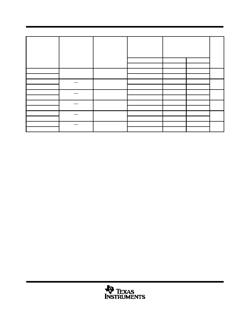
FUNCTION TABLE
INPUTS
OUTPUT
CEAB
LEAB
OEAB
A
B
H
X
X
X
Z
X
X
H
X
Z
L
H
L
X
B0
L
L
L
L
L
L
L
L
H
H
A-to-B data flow is shown; B-to-A flow control is the
same except that it uses CEBA, LEBA, and OEBA.
Output level before the indicated steady-state input
conditions were established.
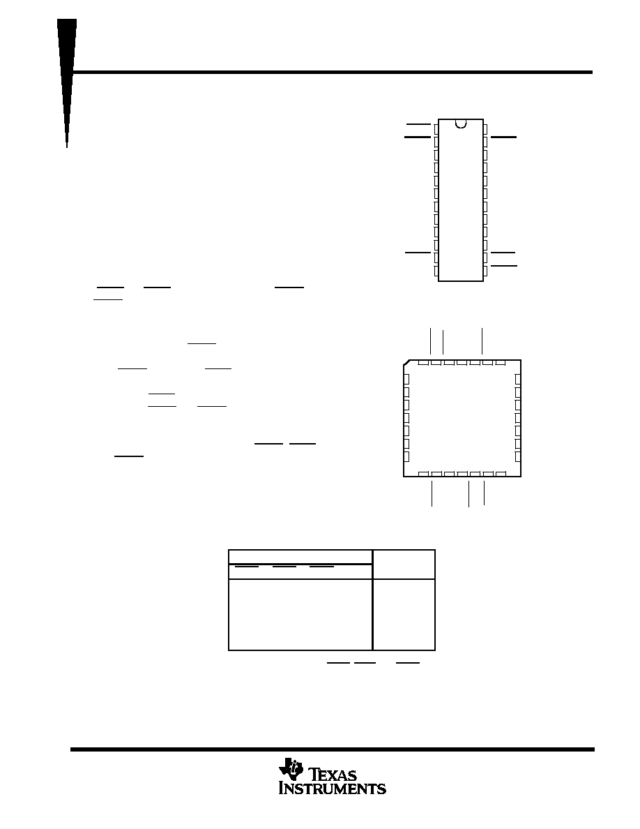
SN54BCT543 . . . JT OR W PACKAGE
SN74BCT543 . . . DW OR NT PACKAGE
(TOP VIEW)
1
2
3
4
5
6
7
8
9
10
11
12
24
23
22
21
20
19
18
17
16
15
14
13
LEBA
OEBA
A1
A2
A3
A4
A5
A6
A7
A8
CEAB
GND
V
CC
CEBA
B1
B2
B3
B4
B5
B6
B7
B8
LEAB
OEAB
SN54BCT543 . . . FK PACKAGE
(TOP VIEW)
3 2 1 28 27
12 13
5
6
7
8
9
10
11
25
24
23
22
21
20
19
B2
B3
B4
NC
B5
B6
B7
A2
A3
A4
NC
A5
A6
A7
4
26
14 15 16 17 18
A8
CEAB
GND
NC
OEAB
LEAB
B8
A1
OEBA
LEBA
NC
CEBA
B1
V
CC
NC ≠ No internal connection
PRODUCTION DATA information is current as of publication date.
Products conform to specifications per the terms of Texas Instruments
standard warranty. Production processing does not necessarily include
testing of all parameters.
SN54BCT543, SN74BCT543
OCTAL REGISTERED TRANSCEIVERS
WITH 3-STATE OUTPUTS
SCBS026C ≠ NOVEMBER 1988 ≠ REVISED APRIL 1994
2≠2
POST OFFICE BOX 655303
∑
DALLAS, TEXAS 75265
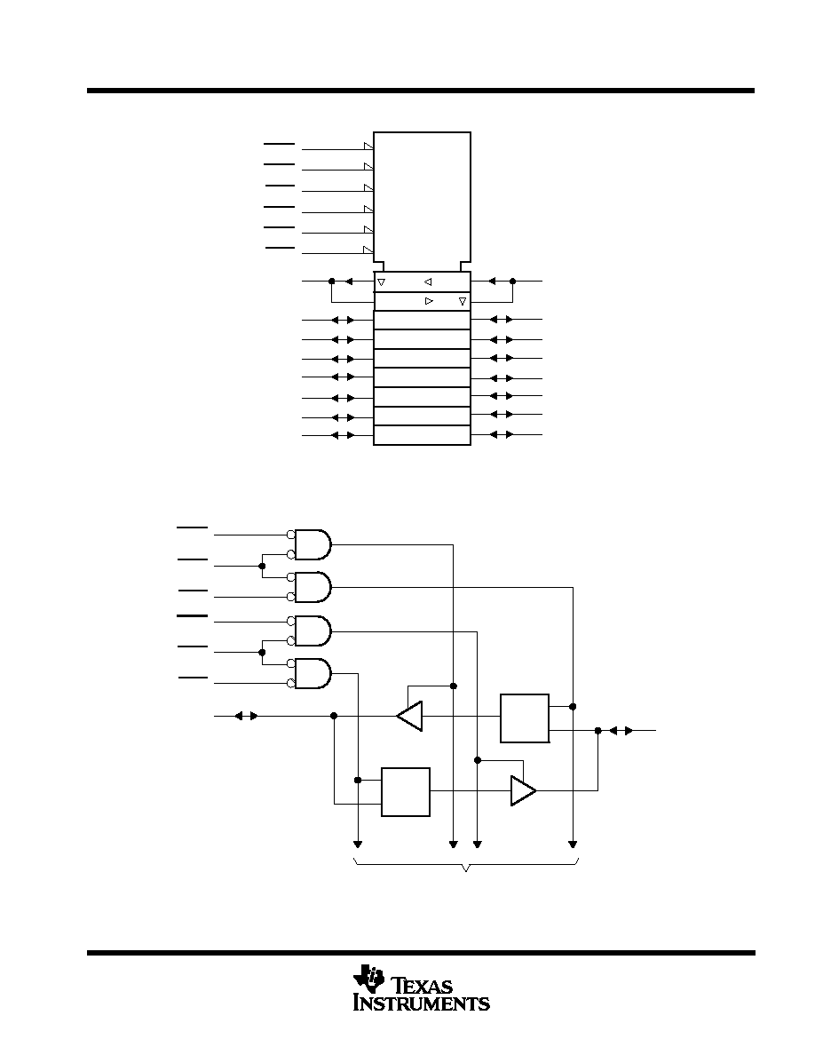
logic symbol
1
1
4
2C6
14
3
A1
4
A2
B1
22
5D
5
A3
6
A4
7
A5
8
A6
9
A7
10
A8
B2
21
B3
20
B5
18
B4
19
B6
17
B8
15
B7
16
LEAB
3
G2
11
CEAB
2EN4
13
OEAB
1C5
1
LEBA
G1
23
CEBA
1EN3
2
OEBA
6D
This symbol is in accordance with ANSI/IEEE Std 91-1984 and IEC Publication 617-12.
logic diagram (positive logic)
OEBA
CEBA
LEBA
OEAB
CEAB
LEAB
A1
B1
C1
1D
C1
1D
2
23
1
13
11
14
3
22
To Seven Other Channels
Pin numbers shown are for the DW, JT, NT, and W packages.
SN54BCT543, SN74BCT543
OCTAL REGISTERED TRANSCEIVERS
WITH 3-STATE OUTPUTS
SCBS026C ≠ NOVEMBER 1988 ≠ REVISED APRIL 1994
2≠3
POST OFFICE BOX 655303
∑
DALLAS, TEXAS 75265
absolute maximum ratings over operating free-air temperature range (unless otherwise noted)
Supply voltage range, V
CC
≠ 0.5 V to 7 V
. . . . . . . . . . . . . . . . . . . . . . . . . . . . . . . . . . . . . . . . . . . . . . . . . . . . . . . . . .
Input voltage range: Control inputs (see Note 1)
≠ 0.5 V to 7 V
. . . . . . . . . . . . . . . . . . . . . . . . . . . . . . . . . . . . . . . .
I/O ports (see Note 1)
≠ 0.5 V to 5.5 V
. . . . . . . . . . . . . . . . . . . . . . . . . . . . . . . . . . . . . . . . . .
Voltage range applied to any output in the disabled or power-off state, V
O
≠ 0.5 V to 7 V
. . . . . . . . . . . . . . . . .
Voltage range applied to any output in the high state, V
O
≠ 0.5 V to V
CC
. . . . . . . . . . . . . . . . . . . . . . . . . . . . . . .
Input clamp current, I
IK
≠30 mA
. . . . . . . . . . . . . . . . . . . . . . . . . . . . . . . . . . . . . . . . . . . . . . . . . . . . . . . . . . . . . . . . . .
Current into any output in the low state: SN54BCT543
96 mA
. . . . . . . . . . . . . . . . . . . . . . . . . . . . . . . . . . . . . . . .
SN74BCT543
128 mA
. . . . . . . . . . . . . . . . . . . . . . . . . . . . . . . . . . . . . . .
Operating free-air temperature range:
SN54BCT543
≠ 55
∞
C to 125
∞
C
. . . . . . . . . . . . . . . . . . . . . . . . . . . . . . . .
SN74BCT543 0
∞
C to 70
∞
C
. . . . . . . . . . . . . . . . . . . . . . . . . . . . . . . . . . . .
Storage temperature range
≠ 65
∞
C to 150
∞
C
. . . . . . . . . . . . . . . . . . . . . . . . . . . . . . . . . . . . . . . . . . . . . . . . . . . . . . . .
Stresses beyond those listed under "absolute maximum ratings" may cause permanent damage to the device. These are stress ratings only, and
functional operation of the device at these or any other conditions beyond those indicated under "recommended operating conditions" is not
implied. Exposure to absolute-maximum-rated conditions for extended periods may affect device reliability.
NOTE 1: The input and output voltage ratings may be exceeded if the input and output current ratings are observed.
recommended operating conditions
SN54BCT543
SN74BCT543
UNIT
MIN
NOM
MAX
MIN
NOM
MAX
UNIT
VCC
Supply voltage
4.5
5
5.5
4.5
5
5.5
V
VIH
High-level input voltage
2
2
V
VIL
Low-level input voltage
0.8
0.8
V
IIK
Input clamp current
≠18
≠18
mA
IOH
High-level output current
≠ 12
≠ 15
mA
IOL
Low-level output current
48
64
mA
TA
Operating free-air temperature
≠ 55
125
0
70
∞
C
SN54BCT543, SN74BCT543
OCTAL REGISTERED TRANSCEIVERS
WITH 3-STATE OUTPUTS
SCBS026C ≠ NOVEMBER 1988 ≠ REVISED APRIL 1994
2≠4
POST OFFICE BOX 655303
∑
DALLAS, TEXAS 75265
electrical characteristics over recommended operating free-air temperature range (unless
otherwise noted)
PARAMETER
TEST CONDITIONS
SN54BCT543
SN74BCT543
UNIT
PARAMETER
TEST CONDITIONS
MIN
TYP
MAX
MIN
TYP
MAX
UNIT
VIK
VCC = 4.5 V,
II = ≠18 mA
≠1.2
≠1.2
V
IOH = ≠ 3 mA
2.4
3.3
2.4
3.3
VOH
VCC = 4.5 V
IOH = ≠12 mA
2
3.2
V
IOH = ≠15 mA
2
3.1
VOL
VCC = 4 5 V
IOL = 48 mA
0.38
0.55
V
VOL
VCC = 4.5 V
IOL = 64 mA
0.42
0.55
V
II
VCC = 5.5 V,
VI = 5.5 V
0.4
0.4
mA
I
A or B port
VCC = 5 5 V
VI = 2 7 V
70
70
µ
A
IIH
Control input
VCC = 5.5 V,
VI = 2.7 V
20
20
µ
A
I
A or B port
VCC = 5 5 V
VI = 0 5 V
≠ 0.65
≠ 0.65
mA
IIL
Control input
VCC = 5.5 V,
VI = 0.5 V
≠ 0.6
≠ 0.6
mA
IOSß
VCC = 5.5 V,
VO = 0
≠100
≠ 225
≠100
≠ 225
mA
ICCL
A or B port
VCC = 5.5 V
45
71
45
71
mA
ICCH
A or B port
VCC = 5.5 V
5
8
5
8
mA
ICCZ
A or B port
VCC = 5.5 V
9
15
9
15
mA
Ci
Control input
VCC = 5 V,
VI = 2.5 V or 0.5 V
6
6
pF
Cio
A or B port
VCC = 5 V,
VO = 2.5 V or 0.5 V
16
16
pF
All typical values are at VCC = 5 V, TA = 25
∞
C.
For I/O ports, the parameters IIH and IIL include the off-state output current.
ß Not more than one output should be tested at a time, and the duration of the test should not exceed one second.
timing requirements over recommended ranges of supply voltage and operating free-air
temperature (unless otherwise noted)
VCC = 5 V,
TA = 25
∞
C
SN54BCT543
SN74BCT543
UNIT
MIN
MAX
MIN
MAX
MIN
MAX
tw
Pulse duration, LEAB or LEBA low
7
8
7
ns
tsu
Setup time, data before LEAB or LEBA
High or low
4.5
5.5
4.5
ns
th
Hold time, data after LEAB or LEBA
High or low
1.5
1.5
1.5
ns
SN54BCT543, SN74BCT543
OCTAL REGISTERED TRANSCEIVERS
WITH 3-STATE OUTPUTS
SCBS026C ≠ NOVEMBER 1988 ≠ REVISED APRIL 1994
2≠5
POST OFFICE BOX 655303
∑
DALLAS, TEXAS 75265
switching characteristics (see Note 2)
PARAMETER
FROM
(INPUT)
TO
(OUTPUT)
VCC = 5 V,
CL = 50 pF,
R1 = 500
,
R2 = 500
,
TA = 25
∞
C
VCC = 4.5 V to 5.5 V,
CL = 50 pF,
R1 = 500
,
R2 = 500
,
TA = MIN to MAX
UNIT
BCT543
SN54BCT543
SN74BCT543
MIN
TYP
MAX
MIN
MAX
MIN
MAX
tPLH
A or B
B or A
2
5.7
7.5
2
9.9
2
8.8
ns
tPHL
A or B
B or A
2
6.3
8.2
2
9.7
2
9.6
ns
tPLH
LE
A or B
2
8.2
10.3
2
13.9
2
12.9
ns
tPHL
LE
A or B
2
8.5
10.6
2
13.2
2
12.7
ns
tPZH
OE
A or B
1
6.8
8.6
1
11.4
1
10.7
ns
tPZL
OE
A or B
1
8.7
10.8
1
12.8
1
12.3
ns
tPHZ
OE
A or B
1
5.5
7.2
1
8.8
1
8.1
ns
tPLZ
OE
A or B
1
4.7
6.4
1
8.1
1
7.2
ns
tPZH
CE
A or B
1
7.6
9.8
1
12.8
1
12
ns
tPZL
CE
A or B
1
9.5
11.6
1
13.8
1
13.5
ns
tPHZ
CE
A or B
1
5.8
7.5
1
9.3
1
8.5
ns
tPLZ
CE
A or B
1
4.8
6.7
1
8.4
1
7.6
ns
For conditions shown as MIN or MAX, use the appropriate value specified under recommended operating conditions.
NOTE 2: Load circuits and voltage waveforms are shown in Section 1.