 | –≠–ª–µ–∫—Ç—Ä–æ–Ω–Ω—ã–π –∫–æ–º–ø–æ–Ω–µ–Ω—Ç: SN65173 | –°–∫–∞—á–∞—Ç—å:  PDF PDF  ZIP ZIP |
SN55173, SN65173, SN75173
QUADRUPLE DIFFERENTIAL LINE RECEIVERS
SLLS144E ≠ OCTOBER 1980 ≠ REVISED APRIL 2000
1
POST OFFICE BOX 655303
∑
DALLAS, TEXAS 75265
D
Meet or Exceed the Requirements of
TIA/EIA-422-B, TIA/EIA-423-B, and
TIA/EIA-485-A and ITU Recommendations
V.10, V.11, X.26, and X.27
D
Designed for Multipoint Bus Transmission
on Long Bus Lines in Noisy Environments
D
3-State Outputs
D
Common-Mode Input Voltage Range of
≠ 12 V to 12 V
D
Input Sensitivity . . .
±
200 mV
D
Input Hysteresis . . . 50 mV Typ
D
High Input Impedance . . . 12 k
Min
D
Operate From Single 5-V Supply
D
Low Power Requirements
D
Pin-to-Pin Replacement for AM26LS32
description
The SN55173, SN65173, and SN75173 are
monolithic quadruple differential line receivers
with 3-state outputs. They are designed to meet
the requirements of TIA/EIA-422-B,
TIA/EIA-423-B, TIA/EIA-485-A, and several ITU
recommendations. The standards are for
balanced multipoint bus transmission at rates up
to 10 megabits per second. The four receivers
share two OR enable inputs, one active when
high, the other active when low. These devices
feature high input impedance, input hysteresis for
increased noise immunity, and input sensitivity of
±
200 mV over a common-mode input voltage
range of ≠ 12 V to 12 V. Fail-safe design specifies
that if the inputs are open circuited, the outputs are
always high. The SN65173 and SN75173 are
designed for optimum performance when used
with the SN75172 or SN75174 quad differential
line drivers.
The SN55173 is characterized over the full military temperature range of ≠ 55
∞
C to 125
∞
C. The SN65173 is
characterized for operation from ≠40
∞
C to 85
∞
C. The SN75173 is characterized for operation from 0
∞
C to 70
∞
C.
Copyright
©
2000, Texas Instruments Incorporated
PRODUCTION DATA information is current as of publication date.
Products conform to specifications per the terms of Texas Instruments
standard warranty. Production processing does not necessarily include
testing of all parameters.
Please be aware that an important notice concerning availability, standard warranty, and use in critical applications of
Texas Instruments semiconductor products and disclaimers thereto appears at the end of this data sheet.
1
2
3
4
5
6
7
8
16
15
14
13
12
11
10
9
1B
1A
1Y
G
2Y
2A
2B
GND
V
CC
4B
4A
4Y
G
3Y
3A
3B
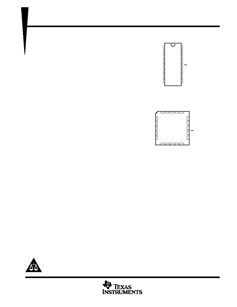
SN55173 . . . J PACKAGE
SN65173, SN75173 . . . D OR N PACKAGE
(TOP VIEW)
3
2
1 20 19
9 10 11 12 13
4
5
6
7
8
18
17
16
15
14
4A
4Y
NC
G
3Y
1Y
G
NC
2Y
2A
SN55173 . . . FK PACKAGE
(TOP VIEW)
1A
1B
NC
3B
3A
4B
2B
GND
NC
NC ≠ No internal connection
V
CC
THE SN55173 IS NOT RECOMMENDED
FOR NEW DESIGNS.
SN55173, SN65173, SN75173
QUADRUPLE DIFFERENTIAL LINE RECEIVERS
SLLS144E ≠ OCTOBER 1980 ≠ REVISED APRIL 2000
2
POST OFFICE BOX 655303
∑
DALLAS, TEXAS 75265
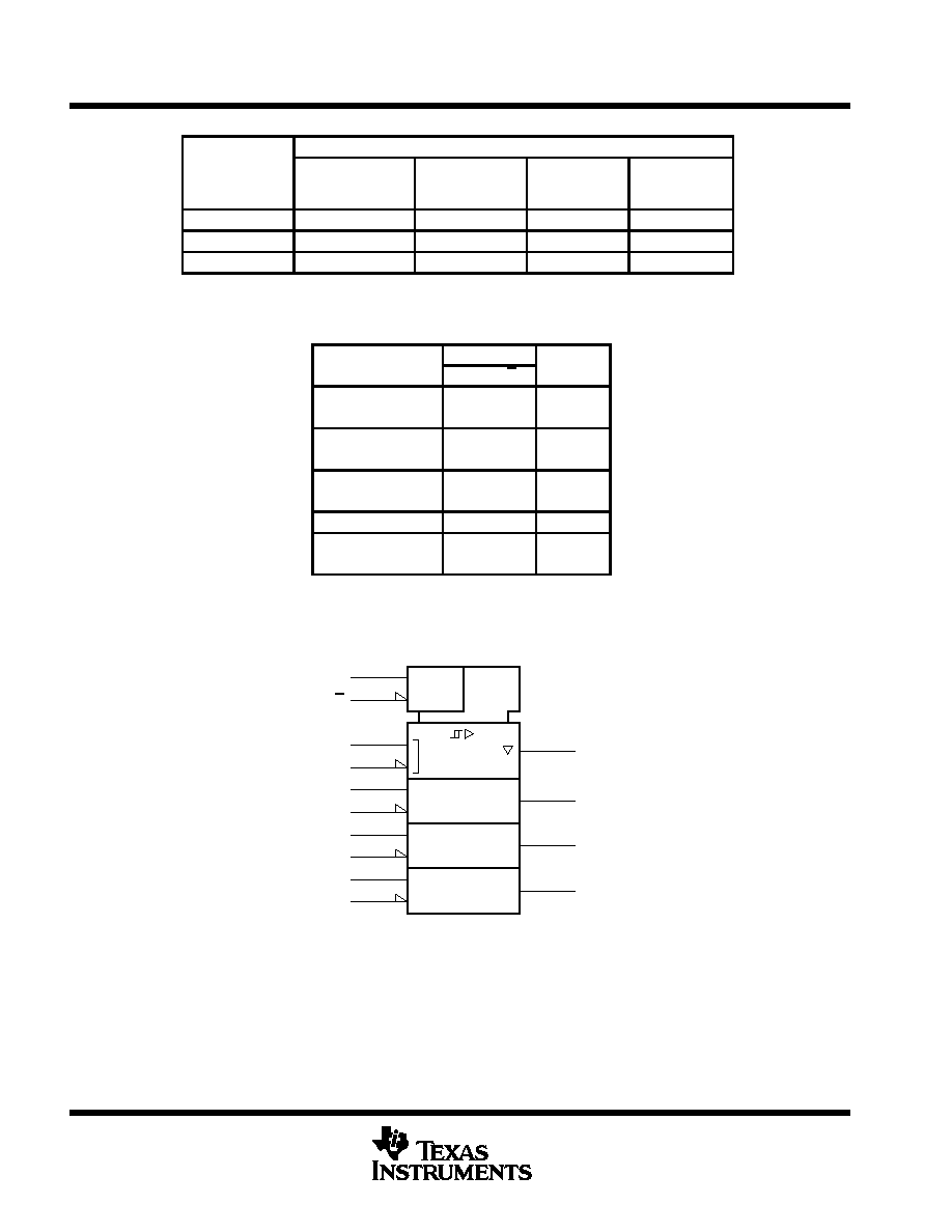
AVAILABLE OPTIONS
PACKAGED DEVICES
TA
PLASTIC
SMALL OUTLINE
(D)
PLASTIC
CHIP CARRIER
(FK)
CERAMIC DIP
(J)
PLASTIC DIP
(N)
0
∞
C to 70
∞
C
SN75173D
--
--
SN75173N
≠40
∞
C to 85
∞
C
SN65173D
--
--
SN65173N
≠55
∞
C to 125
∞
C
--
SN55173FK
SN55173J
--
The D package is available taped and reeled. Add the suffix R to the device type (e.g., SN75173DR).
FUNCTION TABLE
(each receiver)
DIFFERENTIAL
ENABLES
OUTPUT
A≠B
G
G
Y
VID
0 2 V
H
X
H
VID
0.2 V
X
L
H
0 2 V < VID < 0 2 V
H
X
?
≠0.2 V < VID < 0.2 V
X
L
?
VID
0 2 V
H
X
L
VID
≠0.2 V
X
L
L
X
L
H
Z
Open circuit
X
L
H
Open circuit
H
X
H
H = high level, L = low level, ? = indeterminate,
X = irrelevant, Z = high impedance (off)
logic symbol
This symbol is in accordance with ANSI/IEEE Std 91-1984 and IEC Publication 617-12.
4B
4A
3B
3A
2B
2A
1B
1A
G
G
4Y
3Y
2Y
1Y
13
11
5
3
15
14
9
10
7
6
1
2
12
4
EN
Pin numbers shown are for the D, J, and N packages.
1

SN55173, SN65173, SN75173
QUADRUPLE DIFFERENTIAL LINE RECEIVERS
SLLS144E ≠ OCTOBER 1980 ≠ REVISED APRIL 2000
3
POST OFFICE BOX 655303
∑
DALLAS, TEXAS 75265
logic diagram (positive logic)
4Y
3Y
2Y
1Y
13
11
5
3
15
14
9
10
7
6
1
2
12
4
4B
4A
3B
3A
2B
2A
1B
1A
G
G
Pin numbers shown are for the D, J, and N packages.
schematics of inputs and outputs
TYPICAL OF ALL OUTPUTS
EQUIVALENT OF G OR G INPUT
EQUIVALENT OF EACH A OR B INPUT
Output
VCC
8.3 k
NOM
85
NOM
VCC
Input
20 k
NOM
960
NOM
100 k
NOM
B Pins Only
100 k
NOM
A Pins Only
960
NOM
VCC
Input
SN55173, SN65173, SN75173
QUADRUPLE DIFFERENTIAL LINE RECEIVERS
SLLS144E ≠ OCTOBER 1980 ≠ REVISED APRIL 2000
4
POST OFFICE BOX 655303
∑
DALLAS, TEXAS 75265
absolute maximum ratings over operating free-air temperature range (unless otherwise noted)
Supply voltage, V
CC
(see Note 1)
7 V
. . . . . . . . . . . . . . . . . . . . . . . . . . . . . . . . . . . . . . . . . . . . . . . . . . . . . . . . . . . . .
Input voltage (V
I
or B inputs)
±
25 V
. . . . . . . . . . . . . . . . . . . . . . . . . . . . . . . . . . . . . . . . . . . . . . . . . . . . . . . . . . . . . . .
Differential input voltage, V
ID
(see Note 2)
±
25 V
. . . . . . . . . . . . . . . . . . . . . . . . . . . . . . . . . . . . . . . . . . . . . . . . . . .
Enable input voltage, V
I
7 V
. . . . . . . . . . . . . . . . . . . . . . . . . . . . . . . . . . . . . . . . . . . . . . . . . . . . . . . . . . . . . . . . . . . . . .
Low-level output current, I
OL
50
mA
. . . . . . . . . . . . . . . . . . . . . . . . . . . . . . . . . . . . . . . . . . . . . . . . . . . . . . . . . . . . . .
Package thermal impedance,
JA
(see Note 3): D package
73
∞
C/W
. . . . . . . . . . . . . . . . . . . . . . . . . . . . . . . . . . .
N package
67
∞
C/W
. . . . . . . . . . . . . . . . . . . . . . . . . . . . . . . . . . .
Continuous total dissipation
See Dissipation Rating Table
. . . . . . . . . . . . . . . . . . . . . . . . . . . . . . . . . . . . . . . . . . .
Case temperature for 60 seconds, T
C
: FK package
260
∞
C
. . . . . . . . . . . . . . . . . . . . . . . . . . . . . . . . . . . . . . . . . .
Lead temperature 1,6 mm (1/16 inch) from case for 10 seconds: D or N package
260
∞
C
. . . . . . . . . . . . . . . .
Lead temperature 1,6 mm (1/16 inch) from case for 60 seconds: J package
300
∞
C
. . . . . . . . . . . . . . . . . . . . .
Storage temperature range, T
stg
≠ 65
∞
C to 150
∞
C
. . . . . . . . . . . . . . . . . . . . . . . . . . . . . . . . . . . . . . . . . . . . . . . . . . .
Stresses beyond those listed under "absolute maximum ratings" may cause permanent damage to the device. These are stress ratings only, and
functional operation of the device at these or any other conditions beyond those indicated under "recommended operating conditions" is not
implied. Exposure to absolute-maximum-rated conditions for extended periods may affect device reliability.
NOTES:
1. All voltage values, except differential input voltage, are with respect to network ground terminal.
2. Differential input voltage is measured at the noninverting input with respect to the corresponding inverting input.
3. The package thermal impedance is calculated in accordance with JESD 51.
DISSIPATION RATING TABLE
PACKAGE
TA
25
∞
C
POWER RATING
DERATING
FACTOR
TA = 70
∞
C
POWER RATING
TA = 125
∞
C
POWER RATING
FK
1375 mW
11 mW/
∞
C
880 mW
275 mW
J
1375 mW
11 mW/
∞
C
880 mW
275 mW
recommended operating conditions
MIN
NOM
MAX
UNIT
Supply voltage VCC
SN55173
4.5
5
5.5
V
Supply voltage, VCC
SN65173, SN75173
4.75
5
5.25
V
Common-mode input voltage, VIC
±
12
V
Differential input voltage, VID
±
12
V
High-level enable-input voltage, VIH
2
V
Low-level enable-input voltage, VIL
0.8
V
High-level output current, IOH
≠ 400
µ
A
Low-level output current, IOL
16
mA
SN55173
≠ 55
125
Operating free-air temperature, TA
SN65173
≠40
85
∞
C
SN75173
0
70
SN55173, SN65173, SN75173
QUADRUPLE DIFFERENTIAL LINE RECEIVERS
SLLS144E ≠ OCTOBER 1980 ≠ REVISED APRIL 2000
5
POST OFFICE BOX 655303
∑
DALLAS, TEXAS 75265
electrical characteristics over recommended ranges of common-mode input voltage, supply
voltage, and operating free-air temperature
PARAMETER
TEST CONDITIONS
MIN
TYP
MAX
UNIT
VIT+
Positive-going input threshold voltage
VO = 2.7 V,
IO = ≠ 0.4 mA
0.2
V
VIT≠
Negative-going input threshold voltage
VO = 0.5 V,
IO = 16 mA
≠ 0.2
V
Vhys
Hysteresis (VIT+ ≠ VIT≠)
See Figure 4
50
mV
VIK
Enable-input clamp voltage
II = ≠ 18 mA
≠ 1.5
V
SN55173
2.5
V
VOH
High-level output voltage
VID = 200 mV,
IOH = ≠ 400
µ
A
SN65173,
SN75173
2.7
V
VOL
Low level output voltage
VID = 200 mV
See Figure 1
IOL = 8 mA
0.45
V
VOL
Low-level output voltage
VID = ≠ 200 mV,
See Figure 1
IOL = 16 mA
0.5
V
IOZ
High-impedance-state output current
VO = 0.4 V to 2.4 V
±
20
µ
A
II
Line input current
Other input at 0 V
See Note 3
VI = 12 V
1
mA
II
Line input current
Other input at 0 V,
See Note 3
VI = ≠ 7 V
≠ 0.8
mA
IIH
High-level enable-input current
VIH = 2.7 V
20
µ
A
IIL
Low-level enable-input current
VIL = 0.4 V
≠ 100
µ
A
ri
Input resistance
12
k
IOS
Short-circuit output current
≠ 15
≠ 85
mA
ICC
Supply current
Outputs disabled
70
mA
All typical values are at VCC = 5 V, TA = 25
∞
C.
The algebraic convention, in which the less positive (more negative) limit is designated as minimum, is used in this data sheet for threshold voltage
levels only.
NOTE 3: Refer to TIA/EIA-422-B and TIA/EIA-423-B for exact conditions.
switching characteristics, V
CC
= 5 V, T
A
= 25
∞
C
PARAMETER
TEST CONDITIONS
MIN
TYP
MAX
UNIT
tPLH Propagation delay time, low-to-high-level output
VID = ≠ 1.5 V to 1.5 V,
20
35
ns
tPHL Propagation delay time, high-to-low-level output
ID
,
CL = 15 pF,
See Figure 1
22
35
ns
tPZH Output enable time to high level
CL = 15 pF,
See Figure 2
17
22
ns
tPZL
Output enable time to low level
CL = 15 pF,
See Figure 3
20
25
ns
tPHZ Output disable time from high level
CL = 5 pF,
See Figure 2
21
30
ns
tPLZ
Output disable time from low level
CL = 5 pF,
See Figure 3
30
40
ns