
www.ti.com
FEATURES
D, DB, DW, OR PW PACKAGE
(TOP VIEW)
1
2
3
4
5
6
7
8
16
15
14
13
12
11
10
9
C1+
V+
C1-
C2+
C2-
V-
DOUT2
RIN2
V
CC
GND
DOUT1
RIN1
ROUT1
DIN1
DIN2
ROUT2
APPLICATIONS
DESCRIPTION/ORDERING INFORMATION
SN65C3232E,, SN75C3232E
3-V TO 5.5-V TWO-CHANNEL RS-232 1-MBIT/S LINE DRIVERS/RECEIVERS
WITH
±
15-kV IEC ESD PROTECTION
SLLS697 ≠ DECEMBER 2005
∑
Operate With 3-V to 5.5-V V
CC
Supply
∑
Operate up to 1 Mbit/s
∑
Low Supply Current . . . 300
µ
A Typ
∑
External Capacitors . . . 4
◊
0.1
µ
F
∑
Accept 5-V Logic Input With 3.3-V Supply
∑
Latch-Up Performance Exceeds 100 mA Per
JESD 78, Class II
∑
ESD Protection for RS-232 Pins
≠
±
15-kV Human-Body Model (HBM)
≠
±
15-kV IEC 61000-4-2 Air-Gap Discharge
≠
±
8-kV IEC 61000-4-2 Contact Discharge
∑
Battery-Powered Systems
∑
PDAs
∑
Notebooks
∑
Laptops
∑
Palmtop PCs
∑
Hand-Held Equipment
The SN65C3232E and SN75C3232E consist of two line drivers, two line receivers, and a dual charge-pump
circuit with
±
15-kV ESD protection pin to pin (serial-port connection pins, including GND). These devices provide
the electrical interface between an asynchronous communication controller and the serial-port connector. The
charge pump and four small external capacitors allow operation from a single 3-V to 5.5-V supply. The devices
operate at data signaling rates up to 1 Mbit/s and a driver output slew rate of 14 V/
µ
s to 150 V/
µ
s.
ORDERING INFORMATION
T
A
PACKAGE
(1)
ORDERABLE PART NUMBER
TOP-SIDE MARKING
Tube of 40
SN65C3232ED
65C3232
SOIC ≠ D
Reel of 2500
SN65C3232EDR
65C3232
Tube of 40
SN65C3232EDW
SOIC ≠ DW
≠40
∞
C to 85
∞
C
Reel of 2000
SN65C3232EDWR
65C3232
SSOP ≠ DB
Reel of 2000
SN65C3232EDBR
CB3232
Tube of 90
SN65C3232EPW
TSSOP ≠ PW
Reel of 2000
SN65C3232EPWR
75C3232
Tube of 40
SN75C3232ED
SOIC ≠ D
Reel of 2500
SN75C3232EDR
75C3232
Tube of 40
SN75C3232EDW
SOIC ≠ DW
0
∞
C to 70
∞
C
Reel of 2000
SN75C3232EDWR
75C3232
SSOP ≠ DB
Reel of 2000
SN75C3232EDBR
Tube of 90
SN75C3232EPW
TSSOP ≠ PW
CA3232
Reel of 2000
SN75C3232EPWR
(1)
Package drawings, standard packing quantities, thermal data, symbolization, and PCB design guidelines are available at
www.ti.com/sc/package.
Please be aware that an important notice concerning availability, standard warranty, and use in critical applications of Texas
Instruments semiconductor products and disclaimers thereto appears at the end of this data sheet.
PRODUCTION DATA information is current as of publication date.
Copyright © 2005, Texas Instruments Incorporated
Products conform to specifications per the terms of the Texas
Instruments standard warranty. Production processing does not
necessarily include testing of all parameters.

www.ti.com
SN65C3232E,, SN75C3232E
3-V TO 5.5-V TWO-CHANNEL RS-232 1-MBIT/S LINE DRIVERS/RECEIVERS
WITH
±
15-kV IEC ESD PROTECTION
SLLS697 ≠ DECEMBER 2005
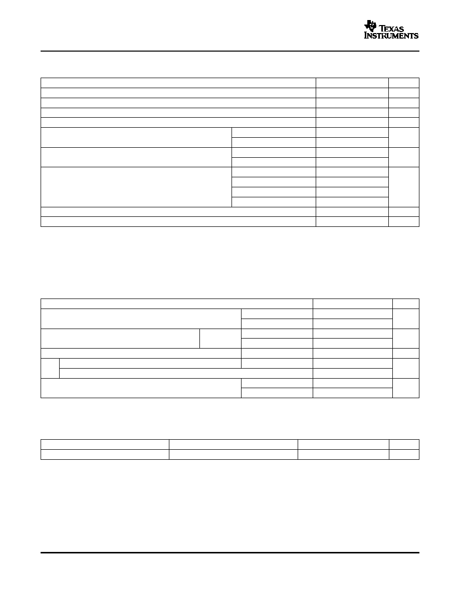
Table 1. 1-Mbit/s RS-232 Parts
SUPPLY
TEMPERATURE
PART
NO. OF
NO. OF
ESD
V
CC
FEATURE
PIN/PACKAGE
RANGE
NO.
DRIVERS
RECEIVERS
(V)
±
15-kV Air-Gap,
16-pin SOIC,
SN65C3221E
1
1
±
8-kV Contact,
3.3 or 5
Auto powerdown
SSOP, TSSOP
±
15-kV HBM
±
15-kV Air-Gap,
16-pin SOIC,
SN65C3232E
2
2
±
8-kV Contact,
3.3 or 5
Low pin count
SSOP, TSSOP
±
15-kV HBM
±
8-kV Air-Gap,
Auto powerdown plus,
MAX3227I
1
1
±
8-kV Contact,
3.3 or 5
16-pin SSOP
ready signal
±
15-kV HBM
16-pin SOIC,
SN65C3221
1
1
±
15-kV HBM
3.3 or 5
Auto powerdown
SSOP, TSSOP
≠40
∞
C to 85
∞
C
Auto powerdown,
20-pin SOIC,
SN65C3223
2
2
±
15-kV HBM
3.3 or 5
enable signal
SSOP, TSSOP
Enable,
20-pin SOIC,
SN65C3222
2
2
±
15-kV HBM
3.3 or 5
powerdown signal
SSOP, TSSOP
16-pin SOIC,
SN65C3232
2
2
±
15-kV HBM
3.3 or 5
Low pin count
SSOP, TSSOP
28-pin SOIC,
SN65C3238
5
3
±
15-kV HBM
3.3 or 5
Auto powerdown plus
SSOP, TSSOP
28-pin SOIC,
SN65C3243
3
5
±
15-kV HBM
3.3 or 5
Auto powerdown
SSOP, TSSOP
±
15-kV Air-Gap,
16-pin SOIC,
SN75C3221E
1
1
±
8-kV Contact,
3.3 or 5
Auto powerdown
SSOP, TSSOP
±
15-kV HBM
±
15-kV Air-Gap,
16-pin SOIC,
SN75C3232E
2
2
±
8-kV Contact,
3.3 or 5
Low pin count
SSOP, TSSOP
±
15-kV HBM
±
8-kV Air-Gap,
Auto powerdown plus,
MAX3227C
1
1
±
8-kV Contact,
3.3 or 5
16-pin SSOP
ready signal
±
15-kV HBM
16-pin SOIC,
SN75C3221
1
1
±
15-kV HBM
3.3 or 5
Auto powerdown
SSOP, TSSOP
0
∞
C to 70
∞
C
Auto powerdown,
20-pin SOIC,
SN75C3223
2
2
±
15-kV HBM
3.5 or 5
enable signal
SSOP, TSSOP
Enable,
20-pin SOIC,
SN75C3222
2
2
±
15-kV HBM
3.3 or 5
powerdown signal
SSOP, TSSOP
16-pin SOIC,
SN75C3232
2
2
±
15-kV HBM
3.3 or 5
Low pin count
SSOP, TSSOP
28-pin SOIC,
SN75C3238
5
3
±
15-kV HBM
3.3 or 5
Auto powerdown plus
SSOP, TSSOP
28-pin SOIC,
SN75C3243
3
5
±
15-kV HBM
3.3 or 5
Auto powerdown
SSOP, TSSOP
2
www.ti.com
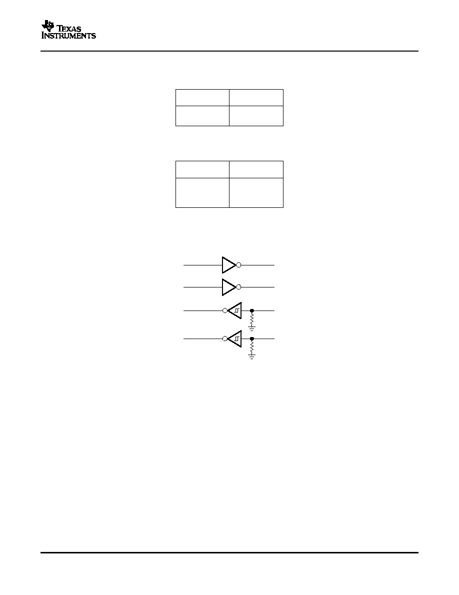
DIN1
DOUT1
RIN1
ROUT1
DIN2
DOUT2
RIN2
ROUT2
11
10
12
9
14
7
13
8
5 k
W
5 k
W
SN65C3232E,, SN75C3232E
3-V TO 5.5-V TWO-CHANNEL RS-232 1-MBIT/S LINE DRIVERS/RECEIVERS
WITH
±
15-kV IEC ESD PROTECTION
SLLS697 ≠ DECEMBER 2005
FUNCTION TABLES
xxx
EACH DRIVER
(1)
INPUT
OUTPUT
DIN
DOUT
L
H
H
L
(1)
H = high level, L = low level
EACH RECEIVER
(1)
INPUT
OUTPUT
RIN
ROUT
L
H
H
L
Open
H
(1)
H = high level, L = low level,
Open = input disconnected or
connected driver off
LOGIC DIAGRAM (POSITIVE LOGIC)
3
www.ti.com
Absolute Maximum Ratings
(1)
Recommended Operating Conditions
(1)
Electrical Characteristics
(1)
SN65C3232E,, SN75C3232E
3-V TO 5.5-V TWO-CHANNEL RS-232 1-MBIT/S LINE DRIVERS/RECEIVERS
WITH
±
15-kV IEC ESD PROTECTION
SLLS697 ≠ DECEMBER 2005
over operating free-air temperature range (unless otherwise noted)
MIN
MAX
UNIT
V
CC
Supply voltage range
(2)
≠0.3
6
V
V+
Positive output supply voltage range
(2)
≠0.3
7
V
V≠
Negative output supply voltage range
(2)
0.3
≠7
V
V+ ≠ V≠
Supply voltage difference
(2)
13
V
Drivers
≠0.3
6
V
I
Input voltage range
V
Receivers
≠25
25
Drivers
≠13.2
13.2
V
O
Output voltage range
V
Receivers
≠0.3
V
CC
+ 0.3
D package
82
DB package
46
JA
Package thermal impedance
(3) (4)
∞
C/W
DW package
57
PW package
108
T
J
Operating virtual junction temperature
150
∞
C
T
stg
Storage temperature range
≠65
150
∞
C
(1)
Stresses beyond those listed under "absolute maximum ratings" may cause permanent damage to the device. These are stress ratings
only, and functional operation of the device at these or any other conditions beyond those indicated under "recommended operating
conditions" is not implied. Exposure to absolute-maximum-rated conditions for extended periods may affect device reliability.
(2)
All voltages are with respect to network GND.
(3)
Maximum power dissipation is a function of T
J
(max),
JA
, and T
A
. The maximum allowable power dissipation at any allowable ambient
temperature is P
D
= (T
J
(max) ≠ T
A
)/
JA
. Operating at the absolute maximum T
J
of 150
∞
C can affect reliability.
(4)
The package thermal impedance is calculated in accordance with JESD 51-7.
MIN
NOM
MAX
UNIT
V
CC
= 3.3 V
3
3.3
3.6
Supply voltage
V
V
CC
= 5 V
4.5
5
5.5
V
CC
= 3.3 V
2
V
IH
Driver high-level input voltage
DIN
V
V
CC
= 5 V
2.4
V
IL
Driver low-level input voltage
DIN
0.8
V
Driver input voltage
DIN
0
5.5
V
I
V
Receiver input voltage
≠25
25
SN65C3232E
≠40
85
T
A
Operating free-air temperature
∞
C
SN75C3232E
0
70
(1)
Test conditions are C1≠C4 = 0.1
µ
F at V
CC
= 3.3 V
±
0.3 V; C1 = 0.047
µ
F, C2≠C4 = 0.33
µ
F at V
CC
= 5 V
±
0.5 V (see
Figure 4
).
over recommended ranges of supply voltage and operating free-air temperature (unless otherwise noted)
PARAMETER
TEST CONDITIONS
MIN
TYP
(2)
MAX
UNIT
I
CC
Supply current
No load,
V
CC
= 3.3 V or 5 V
0.3
1
mA
(1)
Test conditions are C1≠C4 = 0.1
µ
F at V
CC
= 3.3 V
±
0.3 V; C1 = 0.047
µ
F, C2≠C4 = 0.33
µ
F at V
CC
= 5 V
±
0.5 V (see
Figure 4
).
(2)
All typical values are at V
CC
= 3.3 V or V
CC
= 5 V, and T
A
= 25
∞
C.
4

www.ti.com
DRIVER SECTION
Electrical Characteristics
(1)
Switching Characteristics
(1)
ESD Protection
SN65C3232E,, SN75C3232E
3-V TO 5.5-V TWO-CHANNEL RS-232 1-MBIT/S LINE DRIVERS/RECEIVERS
WITH
±
15-kV IEC ESD PROTECTION
SLLS697 ≠ DECEMBER 2005
over recommended ranges of supply voltage and operating free-air temperature (unless otherwise noted)
PARAMETER
TEST CONDITIONS
MIN
TYP
(2)
MAX
UNIT
V
OH
High-level output voltage
DOUT at R
L
= 3 k
to GND,
DIN = GND
5
5.5
V
V
OL
Low-level output voltage
DOUT at R
L
= 3 k
to GND,
DIN = V
CC
≠5
≠5.4
V
I
IH
High-level input current
V
I
= V
CC
±
0.01
±
1
µ
A
I
IL
Low-level input current
V
I
at GND
±
0.01
±
1
µ
A
V
CC
= 3.6 V,
V
O
= 0 V
±
35
±
60
I
OS
(3)
Short-circuit output current
mA
V
CC
= 5.5 V,
V
O
= 0 V
±
35
±
90
r
o
Output resistance
V
CC
, V+, and V≠ = 0 V,
V
O
=
±
2 V
300
10M
(1)
Test conditions are C1≠C4 = 0.1
µ
F at V
CC
= 3.3 V
±
0.3 V; C1 = 0.047
µ
F, C2≠C4 = 0.33
µ
F at V
CC
= 5 V
±
0.5 V (see
Figure 4
) .
(2)
All typical values are at V
CC
= 3.3 V or V
CC
= 5 V, and T
A
= 25
∞
C.
(3)
Short-circuit durations should be controlled to prevent exceeding the device absolute power dissipation ratings, and not more than one
output should be shorted at a time.
over recommended ranges of supply voltage and operating free-air temperature (unless otherwise noted)
PARAMETER
TEST CONDITIONS
MIN TYP
(2)
MAX UNIT
C
L
= 250 pF,
V
CC
= 3 V to 4.5 V
1000
Maximum data rate
R
L
= 3 k
,
kbit/s
(see
Figure 1
)
One DOUT switching
C
L
= 1000 pF,
V
CC
= 3.5 V to 5.5 V
1000
t
sk(p)
Pulse skew
(3)
C
L
= 150 pF to 2500 pF, R
L
= 3 k
to 7 k
, See
Figure 2
300
ns
Slew rate,
SR(tr)
transition region
R
L
= 3 k
to 7 k
, C
L
= 150 pF to 1000 pF, V
CC
= 3.3 V
14
150
V/
µ
s
(see
Figure 1
)
(1)
Test conditions are C1≠C4 = 0.1
µ
F at V
CC
= 3.3 V
±
0.3 V; C1 = 0.047
µ
F, C2≠C4 = 0.33
µ
F at V
CC
= 5 V
±
0.5 V (see
Figure 4
).
(2)
All typical values are at V
CC
= 3.3 V or V
CC
= 5 V, and T
A
= 25
∞
C.
(3)
Pulse skew is defined as |t
PLH
≠ t
PHL
| of each channel of the same device.
TERMINAL
TEST CONDITIONS
TYP
UNIT
NAME
NO.
HBM
±
15
DOUT
7, 14
IEC 61000-4-2 Air-Gap Discharge
±
15
kV
IEC 61000-4-2 Contact Discharge
±
8
5