 | –≠–Ľ–Ķ–ļ—ā—Ä–ĺ–Ĺ–Ĺ—č–Ļ –ļ–ĺ–ľ–Ņ–ĺ–Ĺ–Ķ–Ĺ—ā: SN65HVD23 | –°–ļ–į—á–į—ā—Ć:  PDF PDF  ZIP ZIP |

SN65HVD20, SN65HVD21
SN65HVD22, SN65HVD23, SN65HVD24
SLLS552D - DECEMBER 2002 - REVISED APRIL 2005
EXTENDED COMMON MODE RS 485 TRANSCEIVERS
FEATURES
D
Common-Mode Voltage Range (-20 V to 25 V)
More Than Doubles TIA/EIA-485 Requirement
D
Receiver Equalization Extends Cable Length,
Signaling Rate (HVD23, HVD24)
D
Reduced Unit-Load for up to 256 Nodes
D
Bus I/O Protection to Over 16-kV HBM
D
Failsafe Receiver for Open-Circuit,
Short-Circuit and Idle-Bus Conditions
D
Low Standby Supply Current 1-
Ķ
A Max
D
More Than 100 mV Receiver Hysteresis
APPLICATIONS
D
Long Cable Solutions
-
Factory Automation
-
Security Networks
-
Building HVAC
D
Severe Electrical Environments
-
Electrical Power Inverters
-
Industrial Drives
-
Avionics
DESCRIPTION
The transceivers in the HVD2x family offer performance
far exceeding typical RS-485 devices. In addition to
meeting all requirements of the TIA/EIA-485-A standard,
the HVD2x family operates over an extended range of
common-mode voltage, and has features such as high
ESD protection, wide receiver hysteresis, and failsafe
operation. This family of devices is ideally suited for
long-cable networks, and other applications where the
environment is too harsh for ordinary transceivers.
These devices are designed for bidirectional data
transmission on multipoint twisted-pair cables. Example
applications are digital motor controllers, remote sensors
and terminals, industrial process control, security stations,
and environmental control systems.
These devices combine a 3-state differential driver and a
differential receiver, which operate from a single 5-V power
supply. The driver differential outputs and the receiver
differential inputs are connected internally to form a
differential bus port that offers minimum loading to the bus.
This port features an extended common-mode voltage
range making the device suitable for multipoint
applications over long cable runs.
-20 V
+25 V
-7 V
+12 V
SUPER-485
RS-485
-20 V
-15 V
-10 V
-5 V
0
5 V
10 V
15 V
20 V
25 V
HVD2x Devices Operate Over a Wider Common-Mode Voltage Range
0.1
1
10
100
10
100
1000
HVD20
HVD23
HVD24
HVD21
HVD22
Cable Length - m
Signaling Rate - Mbps
HVD2x APPLICATION SPACE
PRODUCTION DATA information is current as of publication date. Products
conform to specifications per the terms of Texas Instruments standard warranty.
Production processing does not necessarily include testing of all parameters.
Please be aware that an important notice concerning availability, standard warranty, and use in critical applications of Texas Instruments
semiconductor products and disclaimers thereto appears at the end of this data sheet.
www.ti.com
Copyright
2002 - 2003, Texas Instruments Incorporated
SN65HVD20, SN65HVD21
SN65HVD22, SN65HVD23, SN65HVD24
SLLS552D - DECEMBER 2002 - REVISED APRIL 2005
www.ti.com
2
These devices have limited built-in ESD protection. The leads should be shorted together or the device placed in conductive foam during
storage or handling to prevent electrostatic damage to the MOS gates.
DESCRIPTION (continued)
The `HVD20 provides high signaling rate (up to 25 Mbps) for interconnecting networks of up to 64 nodes.
The `HVD21 allows up to 256 connected nodes at moderate data rates (up to 5 Mbps). The driver output slew rate is
controlled to provide reliable switching with shaped transitions which reduce high-frequency noise emissions.
The `HVD22 has controlled driver output slew rate for low radiated noise in emission-sensitive applications and for
improved signal quality with long stubs. Up to 256 `HVD22 nodes can be connected at signaling rates up to 500 kbps.
The `HVD23 implements receiver equalization technology for improved jitter performance on differential bus applications
with data rates up to 25 Mbps at cable lengths up to 160 meters.
The `HVD24 implements receiver equalization technology for improved jitter performance on differential bus applications
with data rates in the range of 1 Mbps to 10 Mbps at cable lengths up to 1000 meters.
The receivers also include a failsafe circuit that provides a high-level output within 250 microseconds after loss of the input
signal. The most common causes of signal loss are disconnected cables, shorted lines, or the absence of any active
transmitters on the bus. This feature prevents noise from being received as valid data under these fault conditions. This
feature may also be used for Wired-Or bus signaling.
The SN65HVD2X devices are characterized for operation over the temperature range of -40
į
C to 85
į
C.
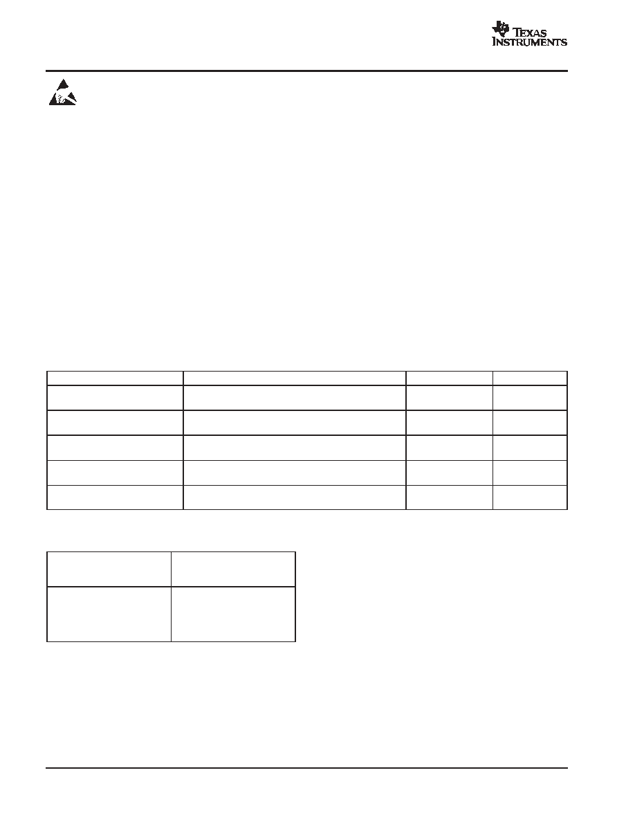
PRODUCT SELECTION GUIDE
PART NUMBERS
CABLE LENGTH AND SIGNALING RATE(1)
NODES
MARKING
SN65HVD20
Up to 50 m at 25 Mbps
Up to 64
D: VP20
P: 65HVD20
SN65HVD21
Up to 150 m at 5 Mbps (with slew rate limit)
Up to 256
D: VP21
P: 65HVD21
SN65HVD22
Up to1200 m at 500 kbps (with slew rate limit)
Up to 256
D: VP22
P: 65HVD22
SN65HVD23
Up to 160 m at 25 Mbps (with receiver equalization)
Up to 64
D: VP23
P: 65HVD23
SN65HVD24
Up to 500 m at 3 Mbps (with receiver equalization)
Up to 256
D: VP24
P: 65HVD24
(1) Distance and signaling rate predictions based upon Belden 3105A cable and 15% eye pattern jitter.
AVAILABLE OPTIONS
PLASTIC THROUGH-HOLE
P-PACKAGE
(JEDEC MS-001)
PLASTIC SMALL-OUTLINE(1)
D-PACKAGE
(JEDEC MS-012)
SN65HVD20P
SN65HVD21P
SN65HVD22P
SN65HVD23P
SN65HVD24P
SN65HVD20D
SN65HVD21D
SN65HVD22D
SN65HVD23D
SN65HVD24D
(1) Add R suffix for taped and reeled carriers.
SN65HVD20, SN65HVD21
SN65HVD22, SN65HVD23, SN65HVD24
SLLS552D - DECEMBER 2002 - REVISED APRIL 2005
www.ti.com
3
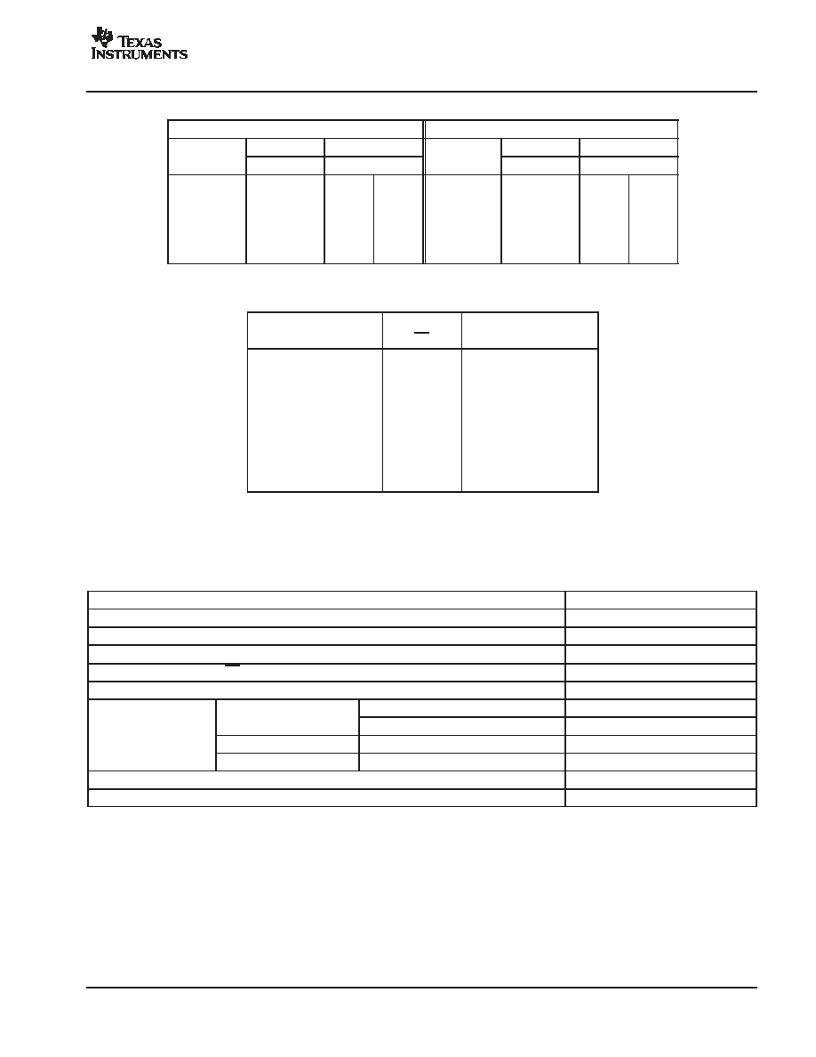
DRIVER FUNCTION TABLE
HVD20, HVD21, HVD22
HVD23, HVD24
INPUT
ENABLE
OUTPUTS
INPUT
ENABLE
OUTPUTS
D
DE
A
B
D
DE
A
B
H
H
H
L
H
H
H
L
L
H
L
H
L
H
L
H
X
L
Z
Z
X
L
Z
Z
X
OPEN
Z
Z
X
OPEN
Z
Z
OPEN
H
H
L
OPEN
H
L
H
H = high level, L= low level, X = don't care, Z = high impedance (off), ? = indeterminate
RECEIVER FUNCTION TABLE
DIFFERENTIAL INPUT
ENABLE
OUTPUT
VID = (VA ≠ VB)
RE
R
0.2 V
VID
L
H
-0.2 V < VID < 0.2 V
L
H (see Note A)
VID
-0.2 V
L
L
X
H
Z
X
OPEN
Z
Open circuit
L
H
Short Circuit
L
H
Idle (terminated) bus
L
H
H = high level, L= low level, Z = high impedance (off)
NOTE A:
If the differential input VID remains within the transition range for
more than 250
Ķ
s, the integrated failsafe circuitry detects a bus
fault, and set the receiver output to a high state. See Figure 15.
ABSOLUTE MAXIMUM RATINGS
over operating free-air temperature range unless otherwise noted(1)
SN65HVD2X
Supply voltage(2), VCC
-0.5 V to 7 V
Voltage at any bus I/O terminal
-27 V to 27 V
Voltage input, transient pulse, A and B, (through 100
, see Figure 16)
-60 V to 60 V
Voltage input at any D, DE or RE terminal
-0.5 V to VCC+ 0.5 V
Receiver output current, IO
-10 mA to 10 mA
Human Body Model(3)
A, B, GND
16 kV
Electrostatic discharge
Human Body Model(3)
All pins
5 kV
Electrostatic discharge
Charged-Device Model(4)
All pins
1.5 kV
Machine Model(5)
All pins
200 V
Continuous total power dissipation
See Power Dissipation Rating Table
Junction temperature, TJ
150
į
C
(1) Stresses beyond those listed under "absolute maximum ratings" may cause permanent damage to the device. These are stress ratings only, and
functional operation of the device at these or any other conditions beyond those indicated under "recommended operating conditions" is not
implied. Exposure to absolute-maximum-rated conditions for extended periods may affect device reliability.
(2) All voltage values, except differential I/O bus voltages, are with respect to network ground terminal.
(3) Tested in accordance with JEDEC Standard 22, Test Method A114-A.
(4) Tested in accordance with JEDEC Standard 22, Test Method C101.
(5) Tested in accordance with JEDEC Standard 22, Test Method A115-A.

SN65HVD20, SN65HVD21
SN65HVD22, SN65HVD23, SN65HVD24
SLLS552D - DECEMBER 2002 - REVISED APRIL 2005
www.ti.com
4
POWER DISSIPATION RATINGS
PACKAGE
CIRCUIT BOARD
MODEL
TA
25
į
C
POWER RATING
DERATING FACTOR(3)
ABOVE TA = 25
į
C
TA = 70
į
C
POWER RATING
TA = 85
į
C
POWER RATING
D
Low-K(1)
577 mW
4.62 mW/
į
C
369 mW
300 mW
D
High-K(2)
913 mW
7.3 mW/
į
C
584 mW
474 mW
P
Low-K(1)
984 mW
7.87 mW/
į
C
630 mW
512 mW
P
High-K(2)
1344 mW
10.8 mW/
į
C
860 mW
700 mW
(1) In accordance with the Low-K thermal metric definitions of EIA/JESD51-3.
(2) In accordance with the High-K thermal metric definitions of EIA/JESD51-7.
(3) This is the inverse of the junction-to-ambient thermal resistance when board-mounted and with no air flow.
THERMAL CHARACTERISTICS
PARAMETER
TEST CONDITIONS
VALUE
UNITS
JB
Junction-to-board thermal resistance
D
86.2
JB
Junction-to-board thermal resistance
P
56
į
C/W
JC
Junction-to-case thermal resistance
D
47.1
į
C/W
JC
Junction-to-case thermal resistance
P
54
HVD20
VCC = 5 V, TJ = 25
į
C,
25 Mbps
295
HVD21
VCC = 5 V, TJ = 25 C,
RL = 54
, CL = 50 pF (driver),
C = 15 pF (receiver),
5 Mbps
260
Typical
HVD22
RL = 54 , CL = 50 pF (driver),
CL = 15 pF (receiver),
50% Duty cycle square-wave signal,
500 kbps
233
Typical
HVD23
50% Duty cycle square-wave signal,
Driver and receiver enabled
25 Mbps
302
PD
Device power dissipation
HVD24
Driver and receiver enabled
5 Mbps
267
mW
PD
Device power dissipation
HVD20
25 Mbps
408
mW
HVD21
VCC = 5.5 V, TJ = 125
į
C,RL = 54
,
C = 50 pF, C = 15 pF (receiver),
5 Mbps
342
Worst case
HVD22
VCC = 5.5 V, TJ = 125 C,RL = 54 ,
CL = 50 pF, CL = 15 pF (receiver),
50% Duty cycle square-wave signal,
500 kbps
300
Worst case
HVD23
50% Duty cycle square-wave signal,
Driver and receiver enabled
25 Mbps
417
HVD24
Driver and receiver enabled
5 Mbps
352
TSD
Thermal shut-down junction temperature
170
į
C
RECOMMENDED OPERATING CONDITIONS
MIN
NOM
MAX
UNIT
Supply voltage, VCC
4.5
5
5.5
V
Voltage at any bus I/O terminal
A, B
-20
25
V
High-level input voltage, VIH
D, DE, RE
2
VCC
V
Low-level input voltage, VIL
D, DE, RE
0
0.8
V
Differential input voltage, VID
A with respect to B
-25
25
V
Output current
Driver
-110
110
mA
Output current
Receiver
-8
8
mA
Operating free-air temperature, TA(1)
-40
85
į
C
Junction temperature, TJ
-40
130
į
C
(1) Maximum free-air temperature operation is allowed as long as the device recommended junction temperature is not exceeded.

SN65HVD20, SN65HVD21
SN65HVD22, SN65HVD23, SN65HVD24
SLLS552D - DECEMBER 2002 - REVISED APRIL 2005
www.ti.com
5
DRIVER ELECTRICAL CHARACTERISTICS
over recommended operating conditions (unless otherwise noted)(1)
PARAMETER
TEST CONDITIONS
MIN
TYP(1)
MAX
UNIT
VIK
Input clamp voltage
II = -18 mA
-1.5
0.75
V
VO
Open-circuit output voltage
A or B, No load
0
VCC
V
Steady-state differential output voltage
No load (open circuit)
3.3
4.2
VCC
VOD(SS)
Steady-state differential output voltage
magnitude
RL = 54
,
See Figure 1
1.8
2.5
V
VOD(SS)
magnitude
With common-mode loading, See Figure 2
1.8
V
|
VOD(SS)|
Change in steady-state differential output
voltage between logic states
See Figure 1 and Figure 3
-0.1
0.1
V
VOC(SS)
Steady-state common-mode output voltage
See Figure 1
2.1
2.5
2.9
V
VOC(SS)
Change in steady-state common-mode output
voltage, VOC(H) ≠ VOC(L)
See Figure 1 and Figure 4
-0.1
0.1
V
VOC(PP)
Peak-to-peak common-mode output voltage,
VOC(MAX) ≠ VOC(MIN)
RL = 54
, CL = 50 pF,
See Figure 1 and Figure 4
0.35
V
VOD(RING)
Differential output voltage over and under shoot
RL = 54
, CL = 50 pF, See Figure 5
10%
II
Input current
D, DE
-100
100
Ķ
A
IO(OFF)
Output current with power off
VCC < = 2.5 V
See receiver line input
IOZ
High impedance state output current
DE at 0 V
See receiver line input
current
IOS
Short-circuit output current
VO = -20 V to 25 V,
See Figure 9
-250
250
mA
COD
Differential output capacitance
See receiver CI
(1) All typical values are at VCC = 5 V and 25
į
C.
DRIVER SWITCHING CHARACTERISTICS
over recommended operating conditions (unless otherwise noted)
PARAMETER
TEST CONDITIONS
MIN
TYP(1)
MAX
UNIT
t
Differential output propagation delay, low-to- high
R = 54 ,
HVD20, HVD23
6
10
20
tPLH
Differential output propagation delay, low-to- high
RL = 54
,
HVD20, HVD23
6
10
20
tPLH
Differential output propagation delay, low-to- high
RL = 54
,
CL = 50 pF,
HVD21, HVD24
20
32
60
ns
t
Differential output propagation delay, high-to-low
CL = 50 pF,
See Figure 3
HVD21, HVD24
20
32
60
ns
tPHL
Differential output propagation delay, high-to-low
CL = 50 pF,
See Figure 3
HVD22
160
280
500
ns
tPHL
Differential output propagation delay, high-to-low
See Figure 3
HVD22
160
280
500
t
Differential output rise time
R = 54 ,
HVD20, HVD23
2
6
12
tr
Differential output rise time
RL = 54
,
HVD20, HVD23
2
6
12
tr
Differential output rise time
RL = 54
,
CL = 50 pF,
HVD21, HVD24
20
40
60
ns
t
Differential output fall time
CL = 50 pF,
See Figure 3
HVD21, HVD24
20
40
60
ns
tf
Differential output fall time
CL = 50 pF,
See Figure 3
HVD22
200
400
600
ns
tf
Differential output fall time
See Figure 3
HVD22
200
400
600
t
Propagation delay time, high-impedance-to-high-level output
HVD20, HVD23
40
tPZH
Propagation delay time, high-impedance-to-high-level output
RE at 0 V,
HVD20, HVD23
40
tPZH
Propagation delay time, high-impedance-to-high-level output
RE at 0 V,
HVD21, HVD24
100
ns
t
Propagation delay time, high-level-output-to-high-impedance
RE at 0 V,
See Figure 6
HVD21, HVD24
100
ns
tPHZ
Propagation delay time, high-level-output-to-high-impedance
See Figure 6
HVD22
300
ns
tPHZ
Propagation delay time, high-level-output-to-high-impedance
See Figure 6
HVD22
300
t
Propagation delay time, high-impedance-to-low-level output
HVD20, HVD23
40
tPZL
Propagation delay time, high-impedance-to-low-level output
RE at 0 V,
HVD20, HVD23
40
tPZL
Propagation delay time, high-impedance-to-low-level output
RE at 0 V,
HVD21, HVD24
100
ns
t
Propagation delay time, low-level-output-to-high-impedance
RE at 0 V,
See Figure 7
HVD21, HVD24
100
ns
tPLZ
Propagation delay time, low-level-output-to-high-impedance
See Figure 7
HVD22
300
ns
tPLZ
Propagation delay time, low-level-output-to-high-impedance
See Figure 7
HVD22
300
td(standby) Time from an active differential output to standby
RE at VCC, See Figure 8
2
Ķ
s
td(wake)
Wake-up time from standby to an active differential output
RE at VCC, See Figure 8
8
Ķ
s
HVD20, HVD23
2
tsk(p)
Pulse skew | tPLH ≠ tPHL |
HVD21, HVD24
6
ns
tsk(p)
Pulse skew | tPLH ≠ tPHL |
HVD22
50
ns
(1) All typical values are at VCC = 5 V and 25
į
C.