SN65LV1021/SN65LV1212
10-MHz TO 40-MHz, 10:1 LVDS SERIALIZER/DESERIALIZER
SLLS526F ≠ FEBRUARY 2002 ≠ REVISED NOVEMBER 2002
1
POST OFFICE BOX 655303
∑
DALLAS, TEXAS 75265
D
100-Mbps to 400-Mbps Serial LVDS Data
Payload Bandwidth at 10-MHz to 40-MHz
System Clock
D
Pin-Compatible Superset of NSM
DS92LV1021/DS92LV1212
D
Chipset (Serializer/Deserializer) Power
Consumption <350 mW (Typ) at 40 MHz
D
Synchronization Mode for Faster Lock
D
Lock Indicator
D
No External Components Required for PLL
D
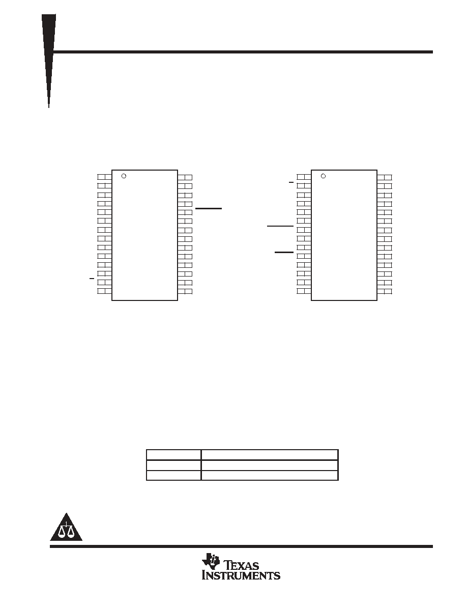
Low-Cost 28-Pin SSOP Package
D
Industrial Temperature Qualified,
T
A
= ≠ 40
∞
C to 85
∞
C
D
Programmable Edge Trigger on Clock
(Rising or Falling Edge)
D
Flow-Through Pinout for Easy PCB Layout
1
2
3
4
5
6
7
8
9
10
11
12
13
14
28
27
26
25
24
23
22
21
20
19
18
17
16
15
SYNC1
SYNC2
D
IN0
D
IN1
D
IN2
D
IN3
D
IN4
D
IN5
D
IN6
D
IN7
D
IN8
D
IN9
TCLK_R/F
TCLK
DV
CC
DV
CC
AV
CC
AGND
PWRDN
AGND
D
O
+
D
O
≠
AGND
DEN
AGND
AV
CC
DGND
DGND
SN65LV1021
Serializer
1
2
3
4
5
6
7
8
9
10
11
12
13
14
28
27
26
25
24
23
22
21
20
19
18
17
16
15
AGND
RCLK_R/F
REFCLK
AV
CC
R
I
+
R
I
≠
PWRDN
REN
RCLK
LOCK
AV
CC
AGND
AGND
DGND
R
OUT0
R
OUT1
R
OUT2
R
OUT3
R
OUT4
DV
CC
DGND
DV
CC
DGND
R
OUT5
R
OUT6
R
OUT7
R
OUT8
R
OUT9
SN65LV1212
Deserializer
description
The SN65LV1021 serializer and SN65LV1212 deserializer comprise a 10-bit serdes chipset designed to
transmit and receive serial data over LVDS differential backplanes at equivalent parallel word rates from 10 MHz
to 40 MHz. Including overhead, this translates into a serial data rate between 120-Mbps and 480-Mbps
payload-encoded throughput.
Upon power up, the chipset link can be initialized via a synchronization mode with internally generated SYNC
patterns, or the deserializer can be allowed to synchronize to random data. By using the synchronization mode,
the deserializer establishes lock within specified, shorter time parameters.
The device can be entered into a power-down state when no data transfer is required. Alternatively, a mode is
available to place the output pins in the high-impedance state without losing PLL lock.
The SN65LV1021 and SN65LV1212 are characterized for operation over ambient air temperature of ≠ 40
∞
C to
85
∞
C.
ORDERING INFORMATION
DEVICE
PART NUMBER
Serializer
SN65LV1021DB
Deserializer
SN65LV1212DB
Copyright
2002, Texas Instruments Incorporated
PRODUCTION DATA information is current as of publication date.
Products conform to specifications per the terms of Texas Instruments
standard warranty. Production processing does not necessarily include
testing of all parameters.
Please be aware that an important notice concerning availability, standard warranty, and use in critical applications of
Texas Instruments semiconductor products and disclaimers thereto appears at the end of this data sheet.

SN65LV1021/SN65LV1212
10-MHz TO 40-MHz, 10:1 LVDS SERIALIZER/DESERIALIZER
SLLS526F ≠ FEBRUARY 2002 ≠ REVISED NOVEMBER 2002
2
POST OFFICE BOX 655303
∑
DALLAS, TEXAS 75265
block diagrams
SYNC1
SYNC2
DEN
A+
A≠
PLL
10
SN65LVDS1021
LVDS
Timing /
Control
Input Latch
Parallel-to-Serial
TCLK_R/F
DIN
Y+
Y≠
PLL
SN65LVDS1212
Timing /
Control
Output Latch
Serial-to-Parallel
Clock
Recovery
10
DOUT
REN
REFCLK
LOCK
RCLK_R/F
RCLK
(10 MHz to
40 MHz)
TCLK
(10 MHz
to
40 MHz)
functional description
The SN65LV1021 and SN65LV1212 are a 10-bit serializer/deserializer chipset designed to transmit data over
differential backplanes or unshielded twisted pair (UTP) at clock speeds from 10 MHz to 40 MHz. The chipset
has five states of operation: initialization mode, synchronization mode, data transmission mode, power-down
mode, and high-impedance mode. The following sections describe each state of operation.
initialization mode
Initialization of both devices must occur before data transmission can commence. Initialization refers to
synchronization of the serializer and deserializer PLLs to local clocks.
When V
CC
is applied to the serializer and/or deserializer, the respective outputs enter the high-impedance state,
while on-chip power-on circuitry disables internal circuitry. When V
CC
reaches 2.45 V, the PLL in each device
begins locking to a local clock. For the serializer, the local clock is the transmit clock (TCLK) provided by an
external source. For the deserializer, a local clock must be applied to the REFCLK pin. The serializer outputs
remain in the high-impedance state, while the PLL locks to the TCLK.

SN65LV1021/SN65LV1212
10-MHz TO 40-MHz, 10:1 LVDS SERIALIZER/DESERIALIZER
SLLS526F ≠ FEBRUARY 2002 ≠ REVISED NOVEMBER 2002
3
POST OFFICE BOX 655303
∑
DALLAS, TEXAS 75265
functional description (continued)
synchronization mode
The deserializer PLL must synchronize to the serializer in order to receive valid data. Synchronization can be
accomplished in one of two ways:
D
Rapid Synchronization: The serializer has the capability to send specific SYNC patterns consisting of six
ones and six zeros switching at the input clock rate. The transmission of SYNC patterns enables the
deserializer to lock to the serializer signal within a deterministic time frame. This transmission of SYNC
patterns is selected via the SYNC1 and SYNC2 inputs on the serializer. Upon receiving valid a SYNC1 or
SYNC2 pulse (wider than 6 clock cycles), 1026 cycles of SYNC pattern are sent.
When the deserializer detects edge transitions at the LVDS input, it attempts to lock to the embedded clock
information. The deserializer LOCK output remains high while its PLL locks to the incoming data or SYNC
patterns present on the serial input. When the deserializer locks to the LVDS data, the LOCK output goes low.
When LOCK is low, the deserializer outputs represent incoming LVDS data. One approach is to tie the
deserializer LOCK output directly to SYNC1 or SYNC2.
D
Random-Lock Synchronization: The deserializer can attain lock to a data stream without requiring the
serializer to send special SYNC patterns. This allows the SN65LV1212 to operate in open-loop applications.
Equally important is the deserializer's ability to support hot insertion into a running backplane. In the
open-loop or hot-insertion case, it is assumed the data stream is essentially random. Therefore, because
lock time varies due to data stream characteristics, the exact lock time cannot be predicted. The primary
constraint on the random lock time is the initial phase relation between the incoming data and the REFCLK
when the deserializer powers up.
The data contained in the data stream can also affect lock time. If a specific pattern is repetitive, the deserializer
could enter false lock--falsely recognizing the data pattern as the start/stop bits. This is referred to as repetitive
multitransition (RMT); see Figure 1 for RMT examples. RMT occurs when more than one low-high transition
takes place per clock cycle over multiple cycles. In the worst case, the deserializer could become locked to the
data pattern rather than the clock. Circuitry within the deserializer can detect that the possibility of false lock
exists. Upon detection, the circuitry prevents the LOCK output from becoming active until the potential false lock
pattern changes. Notice that the RMT pattern only affects the deserializer lock time, and once the deserializer
is in lock, the RMT pattern does not affect the deserializer state as long as the same data boundary happens
each cycle. The deserializer does not go into lock unitil it finds a unique four consecutive cycles of data boundary
(stop/start bits) at the same position.
The deserializer stays in lock until it cannot detect the same data boundary (stop/start bits) for four consecutive
cycles. Then the desiralizer goes out of lock and hunts for the new data boundary (stop/start bits). In the event
of loss of synchronization, the LOCK pin output goes high and the outputs (including RCLK) enter a
high-impedance state. The user's system should monitor the LOCK pin in order to detect a loss of
synchronization. Upon detection of loss of lock, sending sync patterns for resynchronization is desirable if
reestablishing lock within a specific time is critical. However, the deserializer can lock to random data as
previously noted.

SN65LV1021/SN65LV1212
10-MHz TO 40-MHz, 10:1 LVDS SERIALIZER/DESERIALIZER
SLLS526F ≠ FEBRUARY 2002 ≠ REVISED NOVEMBER 2002
4
POST OFFICE BOX 655303
∑
DALLAS, TEXAS 75265
synchronization mode (continued)
Start
Bit
Stop
Bit
DIN0 Held Low and DIN1 Held High
DIN0
DIN1
Start
Bit
Stop
Bit
Start
Bit
Stop
Bit
DIN4 Held Low and DIN5 Held High
DIN4
DIN5
Start
Bit
Stop
Bit
Start
Bit
Stop
Bit
DIN8 Held Low and DIN9 Held High
DIN8
DIN9
Start
Bit
Stop
Bit
Figure 1. RMT Pattern Examples
data transmission mode
After initialization and synchronization, the serializer accepts parallel data from inputs D
IN0
≠ D
IN9
. The serializer
uses the TCLK input to latch the incoming data. The TCLK_R/F pin selects which edge the serializer uses to
strobe incoming data. If either of the SYNC inputs is high for 6 TCLK cycles, the data at D
IN0
≠ D
IN9
is ignored
regardless of the clock edge selected and 1026 cycles of SYNC pattern are sent.
After determining which clock edge to use, a start and stop bit, appended internally, frames the data bits in the
register. The start bit is always high and the stop bit is always low. The start and stop bits function as the
embedded clock bits in the serial stream.
The serializer transmits serialized data and appended clock bits (10+2 bits) from the serial data output (DO
±
)
at 12 times the TCLK frequency. For example, if TCLK is 10 MHz, the serial rate is 10
◊
12 = 120 Mbps. Because
only 10 bits are input data, the useful data rate is 10 times the TCLK frequency. For instance, if TCLK = 12 MHz,
the useful data rate is 10
◊
12 = 120 Mbps. The data source, which provides TCLK, must be in the range of
10 MHz to 40 MHz.

SN65LV1021/SN65LV1212
10-MHz TO 40-MHz, 10:1 LVDS SERIALIZER/DESERIALIZER
SLLS526F ≠ FEBRUARY 2002 ≠ REVISED NOVEMBER 2002
5
POST OFFICE BOX 655303
∑
DALLAS, TEXAS 75265
functional description (continued)
The serializer outputs (DO
±
) can drive point-to-point connections or limited multipoint or multidrop backplanes.
The outputs transmit data when the enable pin (DEN) is high, PWRDN is high, and SYNC1 and SYNC2 are low.
When DEN is driven low, the serializer output pins enter the high-impedance state.
Once the deserializer has synchronized to the serializer, the LOCK pin transitions low. The deserializer locks
to the embedded clock and uses it to recover the serialized data. R
OUTx
data is valid when LOCK is low,
otherwise R
OUT0
≠ R
OUT9
is invalid. The R
OUT0
≠R
OUT9
data is strobed out by RCLK. The specific RCLK edge
polarity to be used is selected by the RCLK_R/F input. The R
OUT0
≠ R
OUT9
, LOCK and RCLK outputs can drive
a maximum of three CMOS input gates (15-pF load, total for all three) with a 40-MHz clock.
power down
When no data transfer is required, the power-down mode can be used. The serializer and deserializer use the
power-down mode, a low-power sleep mode, to reduce power consumption. The deserializer enters power
down when you drive PWRDN and REN low. The serializer enters power down when the PWRDN is driven low.
In power down, the PLL stops and the outputs enter a high-impedance state, which disables load current and
reduces supply current to the milliampere range. To exit power down, you must drive the PWRDN pin high.
Before valid data exchanges between the serializer and deserializer can resume, you must reinitialize and
resynchronize the devices to each other. Initialization of the serializer takes 1026 TCLK cycles. The deserializer
initializes and drives LOCK high until lock to the LVDS clock occurs.
high-impedance mode
The serializer enters the high-impedance mode when the DEN pin is driven low. This puts both driver output
pins (DO+ and DO≠) into a high-impedance state. When you drive DEN high, the serializer returns to its previous
state, as long as all other control pins remain static (SYNC1, SYNC2, PWRDN, TCLK_R/F). When the REN pin
is driven low, the deserializer enters high-impedance mode. Consequently, the receiver output pins
(R
OUT0
≠ R
OUT9
) and RCLK are placed into the high-impedance state. The LOCK output remains active,
reflecting the state of the PLL.
Deserializer Truth Table
INPUTS
OUTPUTS
PWRDN
REN
ROUT[0:9]
LOCK
RCLK
H
H
Z
H
Z
H
H
Active
L
Active
L
X
Z
Z
Z
H
L
Z
Active
Z
NOTES:
1. LOCK output reflects the state of the deserializer with regard
to the selected data stream.
2. RCLK active indicates the RCLK is running if the deserializer
is locked. The timing of RCLK with respect to ROUT is
determined by RCLK_R/F.
3. ROUT and RCLK are 3-stated when LOCK is asserted high.