 | –≠–Ľ–Ķ–ļ—ā—Ä–ĺ–Ĺ–Ĺ—č–Ļ –ļ–ĺ–ľ–Ņ–ĺ–Ĺ–Ķ–Ĺ—ā: SN74AC573 | –°–ļ–į—á–į—ā—Ć:  PDF PDF  ZIP ZIP |
SN54AC573, SN74AC573
OCTAL D-TYPE TRANSPARENT LATCHES
WITH 3-STATE OUTPUTS
SCAS542B - OCTOBER 1995 ≠ REVISED NOVEMBER 1996
1
POST OFFICE BOX 655303
∑
DALLAS, TEXAS 75265
D
3-State Outputs Drive Bus Lines Directly
D
EPIC
TM
(Enhanced-Performance Implanted
CMOS) 1-
Ķ
m Process
D
Package Options Include Plastic
Small-Outline (DW) Shrink Small-Outline
(DB), and Thin Shrink Small-Outline (PW)
Packages, Ceramic Chip Carriers (FK) and
Flatpacks (W), and Standard Plastic (N) and
Ceramic (J) DIPs
description
These 8-bit latches feature 3-state outputs
designed specifically for driving highly capacitive
or relatively low-impedance loads. The devices
are particularly suitable for implementing buffer
registers, I/O ports, bidirectional bus drivers, and
working registers.
The eight latches are D-type transparent latches.
When the latch-enable (LE) input is high, the Q
outputs follow the data (D) inputs. When LE is
taken low, the Q outputs are latched at the logic
levels set up at the D Inputs.
A buffered output-enable (OE) input can be used
to place the eight outputs in either a normal logic
state (high or low logic levels) or the high-imped-
ance state. In the high-impedance state, the
outputs neither load nor drive the bus lines
significantly. The high-impedance state and
increased drive provide the capability to drive bus
lines in a bus-organized system without need for
interface or pullup components.
OE does not affect the internal operations of the latches. Old data can be retained or new data can be entered
while the outputs are in the high-impedance state.
The SN54AC573 is characterized for operation over the full military temperature range of ≠55
_
C to 125
_
C.
The SN74AC573 is characterized for operation from ≠40
_
C to 85
_
C.
FUNCTION TABLE
(each latch)
INPUTS
OUTPUT
OE
LE
D
Q
L
H
H
H
L
H
L
L
L
L
X
Q0
H
X
X
Z
Copyright
©
1996, Texas Instruments Incorporated
EPIC is a trademark of Texas Instruments Incorporated.
UNLESS OTHERWISE NOTED this document contains PRODUCTION
DATA information current as of publication date. Products conform to
specifications per the terms of Texas Instruments standard warranty.
Production processing does not necessarily include testing of all
parameters.
Please be aware that an important notice concerning availability, standard warranty, and use in critical applications of
Texas Instruments semiconductor products and disclaimers thereto appears at the end of this data sheet.
1
2
3
4
5
6
7
8
9
10
20
19
18
17
16
15
14
13
12
11
OE
1D
2D
3D
4D
5D
6D
7D
8D
GND
V
CC
1Q
2Q
3Q
4Q
5Q
6Q
7Q
8Q
LE
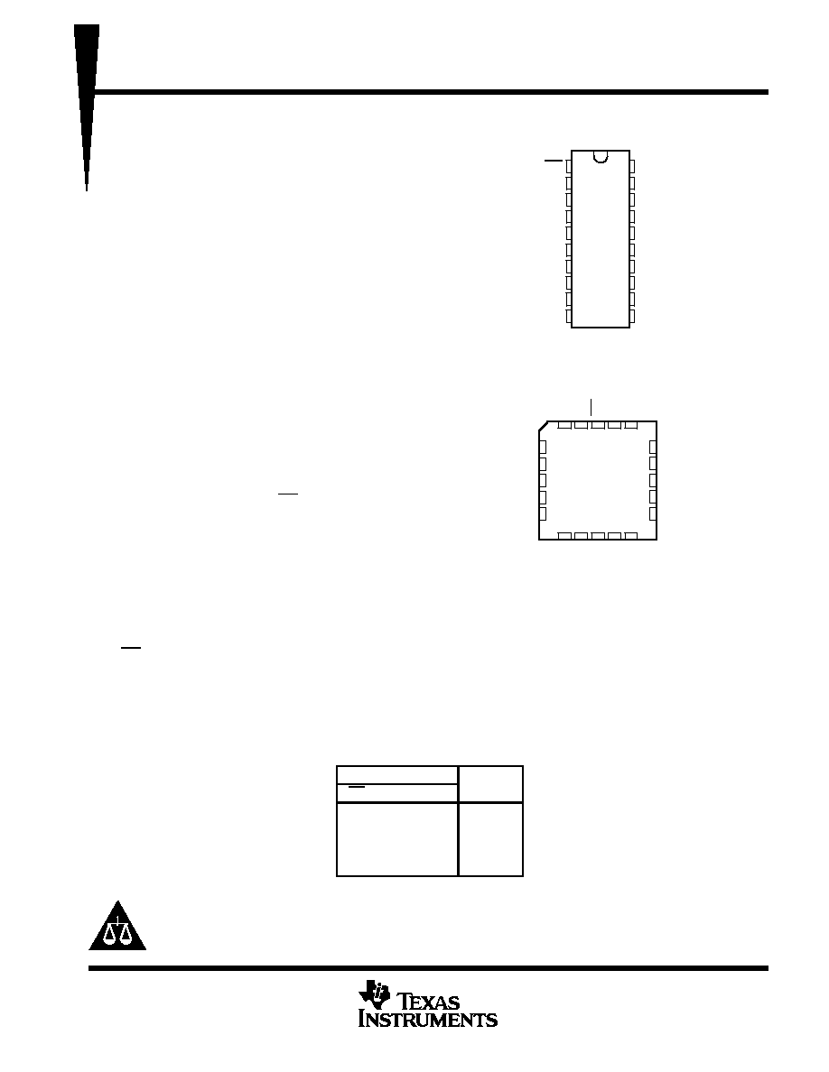
SN54AC573 . . . J OR W PACKAGE
SN74AC573 . . . DB, DW, N, OR PW PACKAGE
(TOP VIEW)
3
2
1 20 19
9 10 11 12 13
4
5
6
7
8
18
17
16
15
14
2Q
3Q
4Q
5Q
6Q
3D
4D
5D
6D
7D
2D
1D
OE
8Q
7Q
1Q
8D
GND
LE
V
CC
SN54AC573 . . . FK PACKAGE
(TOP VIEW)

SN54AC573, SN74AC573
OCTAL D-TYPE TRANSPARENT LATCHES
WITH 3-STATE OUTPUTS
SCAS542B - OCTOBER 1995 ≠ REVISED NOVEMBER 1996
2
POST OFFICE BOX 655303
∑
DALLAS, TEXAS 75265
logic symbol
This symbol is in accordance with ANSI/IEEE Std 91-1984
and IEC Publication 617-12.
OE
1D
2
1D
3
2D
4
3D
5
4D
6
5D
C1
11
LE
1Q
19
2Q
18
3Q
17
4Q
16
5Q
15
6Q
14
7Q
13
8Q
12
7
6D
8
7D
9
8D
EN
1
absolute maximum ratings over operating free-air temperature range (unless otherwise noted)
Supply voltage range, V
CC
≠0.5 V to + 7 V
. . . . . . . . . . . . . . . . . . . . . . . . . . . . . . . . . . . . . . . . . . . . . . . . . . . . . . . . .
Input voltage range, V
I
(see Note 1)
≠0.5 V to V
CC
+ 0.5 V
. . . . . . . . . . . . . . . . . . . . . . . . . . . . . . . . . . . . . . . . . . .
Output voltage range, V
O
(see Note 1)
≠0.5 V to V
CC
+ 0.5 V
. . . . . . . . . . . . . . . . . . . . . . . . . . . . . . . . . . . . . . . .
Input clamp current, I
IK
(V
I
< 0 or V
I
> V
CC
)
Ī
20 mA
. . . . . . . . . . . . . . . . . . . . . . . . . . . . . . . . . . . . . . . . . . . . . . . .
Output clamp current, I
OK
(V
O
< 0 or V
O
> V
CC
)
Ī
20 mA
. . . . . . . . . . . . . . . . . . . . . . . . . . . . . . . . . . . . . . . . . . . .
Continuous output current, I
O
(V
O
= 0 to V
CC
)
Ī
50 mA
. . . . . . . . . . . . . . . . . . . . . . . . . . . . . . . . . . . . . . . . . . . . . .
Continuous current through, V
CC
or GND
Ī
200 mA
. . . . . . . . . . . . . . . . . . . . . . . . . . . . . . . . . . . . . . . . . . . . . . . . .
Maximum power dissipation at T
A
= 55
į
C (in still air) (see Note 2): DB package
0.6 W
. . . . . . . . . . . . . . . . . . .
DW package
1.6 W
. . . . . . . . . . . . . . . . . .
N package
1.3 W
. . . . . . . . . . . . . . . . . . . .
PW package
0.7 W
. . . . . . . . . . . . . . . . . .
Storage temperature range, T
stg
≠65
į
C to 150
į
C
. . . . . . . . . . . . . . . . . . . . . . . . . . . . . . . . . . . . . . . . . . . . . . . . . . .
Stresses beyond those listed under "absolute maximum ratings" may cause permanent damage to the device. These are stress ratings only, and
functional operation of the device at these or any other conditions beyond those indicated under "recommended operating conditions" is not
implied. Exposure to absolute-maximum-rated conditions for extended periods may affect device reliability.
NOTES:
1. The input and output voltage ratings may be exceeded if the input and output current ratings are observed.
2. The maximum package power dissipation is calculated using a junction temperature of 150
_
C and a board trace length of 750 mils,
except for the N package, which has a trace length of zero.
logic diagram (positive logic)
OE
LE
1D
1Q
1
11
2
19
To Seven Other Channels
C1
1D
SN54AC573, SN74AC573
OCTAL D-TYPE TRANSPARENT LATCHES
WITH 3-STATE OUTPUTS
SCAS542B - OCTOBER 1995 ≠ REVISED NOVEMBER 1996
3
POST OFFICE BOX 655303
∑
DALLAS, TEXAS 75265
recommended operating conditions (see Note 3)
SN54AC573
SN74AC573
UNIT
MIN
MAX
MIN
MAX
UNIT
VCC
Supply voltage
2
6
2
6
V
VCC = 3 V
2.1
2.1
VIH
High-level input voltage
VCC = 4.5 V
3.15
3.15
V
VCC = 5.5 V
3.85
3.85
VCC = 3 V
0.9
0.9
VIL
Low-level input voltage
VCC = 4.5 V
1.35
1.35
V
VCC = 5.5 V
1.65
1.65
VI
Input voltage
0
VCC
0
VCC
V
VO
Output voltage
0
VCC
0
VCC
V
VCC = 3 V
≠ 12
≠ 12
IOH
High-level output current
VCC = 4.5 V
≠ 24
≠ 24
mA
VCC = 5.5 V
≠ 24
≠ 24
VCC = 3 V
12
12
IOL
Low-level output current
VCC = 4.5 V
24
24
mA
VCC = 5.5 V
24
24
t/
v
Input transition rise or fall rate
0
8
0
8
ns/V
TA
Operating free-air temperature
≠ 55
125
≠ 40
85
į
C
NOTE 3: Unused inputs must be held high or low to prevent them from floating.
electrical characteristics over recommended operating free-air temperature range (unless
otherwise noted)
PARAMETER
TEST CONDITIONS
VCC
TA = 25
į
C
SN54AC573
SN74AC573
UNIT
PARAMETER
TEST CONDITIONS
VCC
MIN
TYP
MAX
MIN
MAX
MIN
MAX
UNIT
3 V
2.9
2.9
2.9
IOH = ≠ 50
Ķ
A
4.5 V
4.4
4.4
4.4
5.5 V
5.4
5.4
5.4
VOH
IOH = ≠ 12 mA
3 V
2.58
2.48
2.48
V
IOH = 24 mA
4.5 V
3.94
3.8
3.8
IOH = ≠ 24 mA
5.5 V
4.94
4.8
4.8
IOH = ≠ 75 mA
5.5 V
3.85
3.85
3 V
0.1
0.1
0.1
IOL = 50
Ķ
A
4.5 V
0.1
0.1
0.1
5.5 V
0.1
0.1
0.1
VOL
IOL = 12 mA
3 V
0.36
0.44
0.44
V
IOL = 24 mA
4.5 V
0.36
0.44
0.44
IOL = 24 mA
5.5 V
0.36
0.44
0.44
IOL = 75 mA
5.5 V
1.65
1.65
II
VI = VCC or GND
5.5 V
Ī
0.1
Ī
1
Ī
1
Ķ
A
IOZ
VO = VCC or GND
5.5 V
Ī
0.25
Ī
5
Ī
2.5
Ķ
A
ICC
VI = VCC or GND, IO = 0
5.5 V
4
80
40
Ķ
A
Ci
VI = VCC or GND
5 V
5
pF
Not more than one output should be tested at a time, and the duration of the test should not exceed 10 ms.
PRODUCT PREVIEW information concerns products in the formative or
design phase of development. Characteristic data and other
specifications are design goals. Texas Instruments reserves the right to
change or discontinue these products without notice.
SN54AC573, SN74AC573
OCTAL D-TYPE TRANSPARENT LATCHES
WITH 3-STATE OUTPUTS
SCAS542B - OCTOBER 1995 ≠ REVISED NOVEMBER 1996
4
POST OFFICE BOX 655303
∑
DALLAS, TEXAS 75265
timing requirements over recommended operating free-air temperature range, V
CC
= 3.3 V
Ī
0.3 V
(unless otherwise noted) (see Figure 1)
TA = 25
į
C
SN54AC573
SN74AC573
UNIT
MIN
MAX
MIN
MAX
MIN
MAX
UNIT
tw
Pulse duration, LE high
6
8
7
ns
tsu
Setup time, data before LE
3.5
5
4
ns
th
Hold time, data after LE
2
3
2
ns
timing requirements over recommended operating free-air temperature range, V
CC
= 5 V
Ī
0.5 V
(unless otherwise noted) (see Figure 1)
TA = 25
į
C
SN54AC573
SN74AC573
UNIT
MIN
MAX
MIN
MAX
MIN
MAX
UNIT
tw
Pulse duration, LE high
4
6
5
ns
tsu
Setup time, data before LE
3
4.5
3.5
ns
th
Hold time, data after LE
2
3
2
ns
switching characteristics over recommended operating free-air temperature range,
V
CC
= 3 V
Ī
0.3 V (unless otherwise noted) (see Figure 1)
PARAMETER
FROM
TO
TA = 25
į
C
SN54AC573
SN74AC573
UNIT
PARAMETER
(INPUT)
(OUTPUT)
MIN
MAX
MIN
MAX
MIN
MAX
UNIT
tPLH
D
Q
2.5
13
1.5
16.5
2
15
ns
tPHL
D
Q
2.5
12
1.5
15.5
2
14
ns
tPLH
LE
Q
2.5
13
1.5
16.5
2
15
ns
tPHL
LE
Q
2.5
12
1.5
15.5
2
14
ns
tPZH
OE
Q
2.5
11
1.5
13.5
2
12
ns
tPZL
OE
Q
2.5
11
1.5
14
2
12.5
ns
tPHZ
OE
Q
2.5
12.5
1.5
15
2
13.5
ns
tPLZ
OE
Q
2.5
9.5
1.5
12
2
10.5
ns
switching characteristics over recommended operating free-air temperature range,
V
CC
= 5 V
Ī
0.5 V (unless otherwise noted) (see Figure 1)
PARAMETER
FROM
TO
TA = 25
į
C
SN54AC573
SN74AC573
UNIT
PARAMETER
(INPUT)
(OUTPUT)
MIN
MAX
MIN
MAX
MIN
MAX
UNIT
tPLH
D
Q
2.5
10
1.5
13
2
11.5
ns
tPHL
D
Q
2.5
9.5
1.5
12.5
2
11
ns
tPLH
LE
Q
2.5
9.5
1.5
12.5
2
11
ns
tPHL
LE
Q
2.5
8.5
1.5
11.5
2
10
ns
tPZH
OE
Q
2.5
9
1.5
11.5
2
10
ns
tPZL
OE
Q
2.5
8.5
1.5
11
2
9.5
ns
tPHZ
OE
Q
2.5
11
1.5
13.5
2
12
ns
tPLZ
OE
Q
2.5
8
1.5
10.5
2
9
ns
operating characteristics, V
CC
= 5 V, T
A
= 25
į
C
PARAMETER
TEST CONDITIONS
TYP
UNIT
Cpd
Power dissipation capacitance
CL = 50 pF, f = 1 MHz
25
pF
PRODUCT PREVIEW information concerns products in the formative or
design phase of development. Characteristic data and other
specifications are design goals. Texas Instruments reserves the right to
change or discontinue these products without notice.
SN54AC573, SN74AC573
OCTAL D-TYPE TRANSPARENT LATCHES
WITH 3-STATE OUTPUTS
SCAS542B - OCTOBER 1995 ≠ REVISED NOVEMBER 1996
5
POST OFFICE BOX 655303
∑
DALLAS, TEXAS 75265
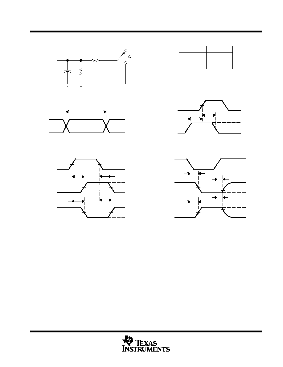
PARAMETER MEASUREMENT INFORMATION
50% VCC
50% VCC
50% VCC
50% VCC
VCC
VCC
0 V
0 V
th
tsu
VOLTAGE WAVEFORMS
Data Input
tPLH
tPHL
tPHL
tPLH
VOH
VOH
VOL
VOL
VCC
0 V
50% VCC
50% VCC
Input
Out-of-Phase
Output
In-Phase
Output
Timing Input
50% VCC
VOLTAGE WAVEFORMS
From Output
Under Test
CL = 50 pF
(see Note A)
LOAD CIRCUIT
S1
2
◊
VCC
500
500
Output
Control
(low-level
enabling)
Output
Waveform 1
S1 at 2
◊
VCC
(see Note B)
Output
Waveform 2
S1 at Open
(see Note B)
VOL
VOH
tPZL
tPZH
tPLZ
tPHZ
[
VCC
0 V
50% VCC
VOL + 0.3 V
50% VCC
[
0 V
Open
VOLTAGE WAVEFORMS
tPLH/tPHL
tPLZ/tPZL
tPHZ/tPZH
Open
2
◊
VCC
Open
TEST
S1
3 V
0 V
tw
VOLTAGE WAVEFORMS
Input
50% VCC
50% VCC
VOH ≠ 0.3 V
50% VCC
50% VCC
50% VCC
50% VCC
VCC
GND
NOTES: A. CL includes probe and jig capacitance.
B. Waveform 1 is for an output with internal conditions such that the output is low except when disabled by the output control.
Waveform 2 is for an output with internal conditions such that the output is high except when disabled by the output control.
C. All input pulses are supplied by generators having the following characteristics: PRR
1 MHz, ZO = 50
, tr
2.5 ns, tf
2.5 ns.
D. The outputs are measured one at a time with one input transition per measurement.
Figure 1. Load Circuit and Voltage Waveforms