SN74ACT2235
1024
◊
9
◊
2
ASYNCHRONOUS BIDIRECTIONAL FIRST-IN, FIRST-OUT MEMORY
SCAS148E ≠ DECEMBER 1990 ≠ REVISED APRIL 1998
1
POST OFFICE BOX 655303
∑
DALLAS, TEXAS 75265
D
Independent Asynchronous Inputs and
Outputs
D
Low-Power Advanced CMOS Technology
D
Bidirectional
D
Dual 1024 by 9 Bits
D
Programmable Almost-Full/Almost-Empty
Flag
D
Empty, Full, and Half-Full Flags
D
Access Times of 25 ns With a 50-pF Load
D
Data Rates up to 50 MHz
D
Fall-Through Times of 22 ns Maximum
D
High Output Drive for Direct Bus Interface
D
Package Options Include 44-Pin Plastic
Leaded Chip Carriers (FN) and 64-Pin Thin
Quad Flat (PAG, PM) Packages
description
A FIFO memory is a storage device that allows data to be written into and read from its array at independent
data rates. The SN74ACT2235 is arranged as two 1024 by 9-bit FIFOs for high speed and fast access times.
It processes data at rates up to 50 MHz, with access times of 25 ns in a bit-parallel format.
The SN74ACT2235 consists of bus-transceiver circuits, two 1024
◊
9 FIFOs, and control circuitry arranged for
multiplexed transmission of data directly from the data bus or from the internal FIFO memories. Enable (GAB
and GBA) inputs are provided to control the transceiver functions. The select-control (SAB and SBA) inputs are
provided to select whether real-time or stored data is transferred. The circuitry used for select control eliminates
the typical decoding glitch that occurs in a multiplexer during the transition between stored and real-time data.
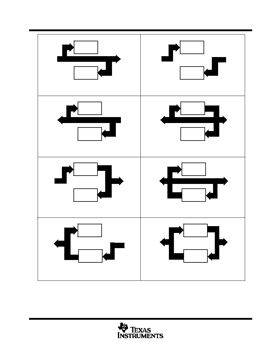
Figure 2 shows the eight fundamental bus-management functions that can be performed with the
SN74ACT2235.
For more information on this device family, see the application report,
1K
◊
9
◊
2 Asynchronous FIFO
SN74ACT2235, literature number SCAA010.
The SN74ACT2235 is characterized for operation from 0
∞
C to 70
∞
C.
B2
B3
B4
V
CC
B5
B6
B7
B8
GND
AF/AEB
HFB
39
38
37
36
35
34
33
32
31
30
29
18 19
7
8
9
10
11
12
13
14
15
16
17
A3
A4
V
CC
A5
A6
A7
A8
GND
AF/AEA
HFA
LDCKA
20 21 22 23
FN PACKAGE
(TOP VIEW)
GAB
GND
B0
B1
5 4
3
2 1
6
44
A2
A1
A0
GND
GBA
SBA
SAB
EMPTY
A
UNCKA
FULLB
LDCKB
FULLA
UNCKB
EMPTYB
DAF
RST
A
RSTB
DBF
42 41 40
43
24 25 26 27 28
Copyright
©
1998, Texas Instruments Incorporated
PRODUCTION DATA information is current as of publication date.
Products conform to specifications per the terms of Texas Instruments
standard warranty. Production processing does not necessarily include
testing of all parameters.
Please be aware that an important notice concerning availability, standard warranty, and use in critical applications of
Texas Instruments semiconductor products and disclaimers thereto appears at the end of this data sheet.

SN74ACT2235
1024
◊
9
◊
2
ASYNCHRONOUS BIDIRECTIONAL FIRST-IN, FIRST-OUT MEMORY
SCAS148E ≠ DECEMBER 1990 ≠ REVISED APRIL 1998
2
POST OFFICE BOX 655303
∑
DALLAS, TEXAS 75265
V
CC
V
CC
A3
A4
V
CC
GND
GND
A5
A6
V
CC
V
CC
A7
A8
GND
GND
AF/AEA
HFA
A1
A0
GND
GBA
A2
GND
SBA
GND
B1
B2
SAB
B0
EMPTYB
UNCKA
FULLA
DAF
EMPTY
A
LDCKB
NC
NC
LDCKA
NC
FULLB
RSTB
DBF
UNCKB
RST
A
NC
GND
GAB
17 18 19 20 21 22
25 26 27 28 29 30 31 32
24
23
64 63 62 61 60 59 58 57 56 55 54 53 52 51 50 49
PAG OR PM PACKAGE
(TOP VIEW)
NC
V
CC
B3
B4
GND
GND
V
CC
B5
B6
V
CC
B7
B8
GND
GND
AF/AEB
HFB
NC ≠ No internal connection
V
CC
1
2
3
4
5
6
7
8
9
10
11
12
13
14
15
16
48
47
46
45
44
43
42
41
40
39
38
37
36
35
34
33

SN74ACT2235
1024
◊
9
◊
2
ASYNCHRONOUS BIDIRECTIONAL FIRST-IN, FIRST-OUT MEMORY
SCAS148E ≠ DECEMBER 1990 ≠ REVISED APRIL 1998
3
POST OFFICE BOX 655303
∑
DALLAS, TEXAS 75265
logic symbol
26
UNCKA
LDCKA
A1
24
DEF B FLAG
20
EMPTYB
DEF A FLAG
21
EMPTYA
25
FULLA
18
17
LDCKA
UNCKA
Reset A
22
EN2
2
GBA
EN1
43
GAB
0
1
SBA
1
44
SAB
27
FULL B
UNCKB
19
LDCKB
28
23
RESET B
LDCKB
UNCKB
FIFO
1024
◊
9
◊
2
SN74ACT2235
A2
A3
A4
A5
A6
A7
B1
B2
B3
B4
B5
B6
B7
40
39
38
37
35
34
33
5
6
7
8
10
11
12
A8
13
B8
32
MODE
ALMOST-FULL/
15
AF/AEA
ALMOST-EMPTY A
AF/AEB
30
ALMOST-FULL/
ALMOST-EMPTY A
0
4
A0
B0
41
0
8
8
A Data
B Data
HALF-FULL A
16
HFA
HFB
29
HALF-FULL B
RSTA
DAF
FULLA
EMPTYA
RSTB
DBF
FULLB
EMPTYB
This symbol is in accordance with ANSI/IEEE Std 91-1984 and IEC Publication 617-12.
Pin numbers shown are for the FN package.

SN74ACT2235
1024
◊
9
◊
2
ASYNCHRONOUS BIDIRECTIONAL FIRST-IN, FIRST-OUT MEMORY
SCAS148E ≠ DECEMBER 1990 ≠ REVISED APRIL 1998
4
POST OFFICE BOX 655303
∑
DALLAS, TEXAS 75265
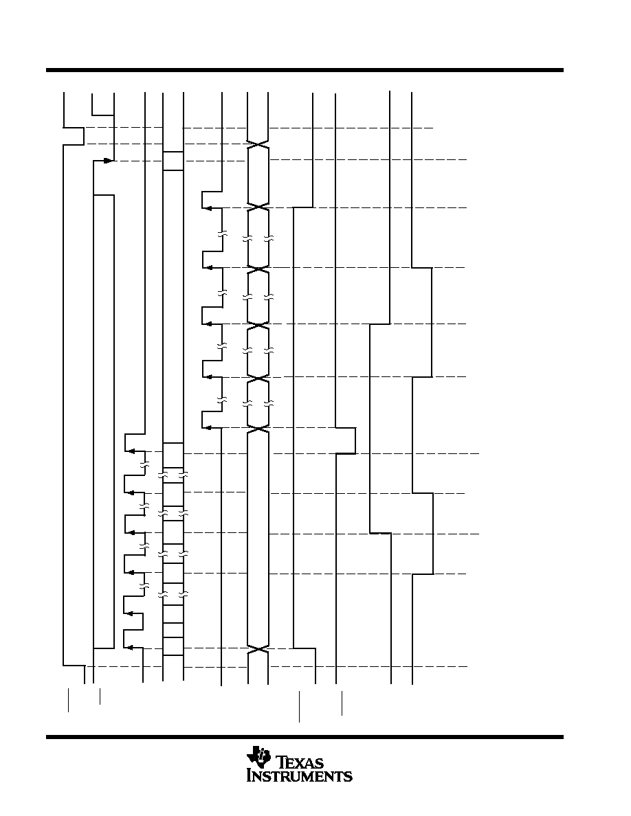
logic diagram (positive logic)
Q
D
B0
Q
D
One of Nine Channels
SAB
SBA
EMPTYB
UNCKB
GBA
GAB
RSTA
DAF
FULLA
LDCKA
A0
RSTB
DBF
FULLB
LDCKB
To Other Channels
One of Nine Channels
To Other Channels
EMPTYA
UNCKA
AF/AEA
AF/AEB
HFB
FIFO A
1024
◊
9
HFA
FIFO B
1024
◊
9

SN74ACT2235
1024
◊
9
◊
2
ASYNCHRONOUS BIDIRECTIONAL FIRST-IN, FIRST-OUT MEMORY
SCAS148E ≠ DECEMBER 1990 ≠ REVISED APRIL 1998
5
POST OFFICE BOX 655303
∑
DALLAS, TEXAS 75265
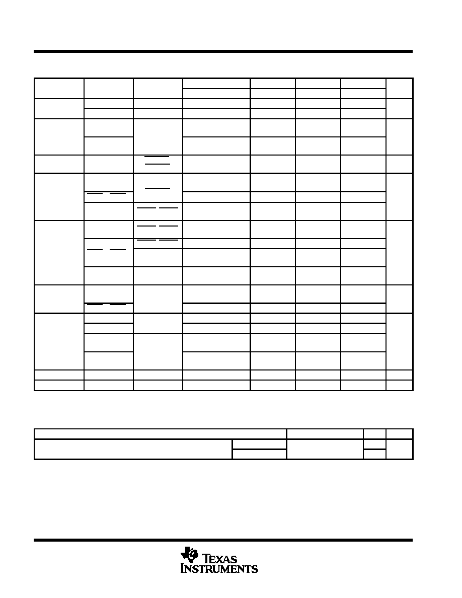
Terminal Functions
TERMINAL
I/O
DESCRIPTION
NAME
NO.
I/O
DESCRIPTION
AF/AEA
AF/AEB
15
30
O
Almost full/almost empty flags. The almost-full/almost-empty A flag (AF/AEA) is defined by the
almost-full/almost-empty offset value for FIFO A (X). AF/AEA is high when FIFO A contains X or fewer words
or 1024≠X words. AF/AEA is low when FIFO A contains between (X + 1) or (1023 ≠ X) words. The operation
of the almost-full/almost-empty B flag (AF/AEB) is the same as AF/AEA for FIFO B.
A0≠A8
4≠8,
10≠13
I/O
A-data inputs and outputs
B0≠B8
32≠35,
37≠41
I/O
B-data inputs and outputs
DAF
DBF
21
24
I
Define-flag inputs. The high-to-low transition of DAF stores the binary value on A0≠A8 as the
almost-full/almost-empty offset value for FIFO A (X). The high-to-low transition of DBF stores the binary value
of B0≠B8 as the almost-full/almost-empty offset value for FIFO B (Y).
EMPTYA
EMPTYB
20
25
O
Empty flags. EMPTYA and EMPTYB are low when their corresponding memories are empty and high when
they are not empty.
FULLA
FULLB
18
27
O
Full flags. FULLA and FULLB are low when their corresponding memories are full and high when they are
not full.
HFA
HFB
16
29
O
Half-full flags. HFA and HFB are high when their corresponding memories contain 512 or more words and
low when they contain 511 or fewer words.
LDCKA
LDCKB
17
28
I
Load clocks. Data on A0≠A8 is written into FIFO A on a low-to-high transition of LDCKA. Data on B0≠B8 is
written into FIFO B on a low-to-high transition of LDCKB. When the FIFOs are full, LDCKA and LDCKB have
no effect on the data residing in memory.
GAB
GBA
2
43
I
Output enables. GAB, GBA control the transceiver functions. When GBA is low, A0≠A8 are in the
high-impedance state. When GAB is low, B0≠B8 are in the high-impedance state.
RSTA
RSTB
22
23
I
Reset. A reset is accomplished in each direction by taking RSTA and RSTB low. This sets EMPTYA,
EMPTYB, FULLA, FULLB, and AF/AEB high. Both FIFOs must be reset upon power up.
SAB
SBA
1
44
I
Select-control inputs. SAB and SBA select whether real-time or stored data is transferred. A low level selects
real-time data and a high level selects stored data. Eight fundamental bus-management functions can be
performed as shown in Figure 2.
UNCKA
UNCKB
19
26
I
Unload clocks. Data in FIFO A is read to B0≠B8 on a low-to-high transition of UNCKB. Data in FIFO B is read
to A0≠A8 on a low-to-high transition of UNCKB. When the FIFOs are empty, UNCKA and UNCKB have no
effect on data residing in memory.
Terminals listed are for the FN package.
programming procedure for AF/AEA
The almost-full/almost-empty flags (AF/AEA, AF/AEB) are programmed during each reset cycle. The
almost-full/almost-empty offset value for FIFO A (X) and for FIFO B (Y) is either a user-defined value or the
default values of X = 256 and Y = 256. Below are instructions to program AF/AEA using both methods. AF/AEB
is programmed in the same manner for FIFO B.
user-defined X
Take DAF from high to low. This stores A0≠A8 as X.
If RSTA is not already low, take RSTA low.
With DAF held low, take RSTA high. This defines AF/AEA using X.
To retain the current offset for the next reset, keep DAF low.
default X
To redefine AF/AE using the default value of X = 256, hold DAF high during the reset cycle.
Figure 1
SN74ACT2235
1024
◊
9
◊
2
ASYNCHRONOUS BIDIRECTIONAL FIRST
-IN, FIRST
-OUT
MEMOR
Y
SCAS148E
≠ DECEMBER 1990 ≠ REVISED APRIL 1998
6
POST
OFFICE BOX 655303
∑
DALLAS, TEXAS 75265
ŒŒ
ŒŒ
ŒŒ
ŒŒ
ŒŒ
ŒŒ
ŒŒ
ŒŒ
ŒŒ
ŒŒ
ŒŒ
ŒŒ
ŒŒ
……
ŒŒ
ŒŒ
ŒŒ
ŒŒ
ŒŒ
ŒŒ
ŒŒ
ŒŒ
ŒŒ
ŒŒ
ŒŒ
ŒŒ
ŒŒ
ŒŒ
ŒŒ
ŒŒ
ŒŒ
ŒŒ
ŒŒ
FULLA
EMPTYA
A0≠A8
DAF
Q0≠Q8
AF/AEA
ŒŒŒ
ŒŒŒ
ŒŒŒ
ŒŒŒ
ŒŒŒ
ŒŒŒ
ŒŒŒ
ŒŒŒ
ŒŒŒ
ŒŒŒ
ŒŒŒ
ŒŒŒ
ŒŒŒ
ŒŒŒ
ŒŒŒ
ŒŒŒ
ŒŒŒ
ŒŒŒ
ŒŒŒ
ŒŒŒ
ŒŒŒ
ŒŒŒ
ŒŒŒ
ŒŒŒ
ŒŒŒ
ŒŒŒ
ŒŒŒ
ŒŒŒ
ŒŒŒ
Don't Care
HFA
LDCKA
UNCKA
Don't Care
Word
RSTA
Word
1
Word
2
Word
257
Word 1
Word
2
Word
257
Word
512
Word
768
Word
1024
Word
513
Word
258
Word
514
Word
768
Word
769
Word
1024
ŒŒŒ
ŒŒŒ
ŒŒŒ
Invalid
Invalid
Set Flag to Empty + 256/
Full ≠ 256 (default)
Empty + 256
Full
Half Full
Full ≠ 256
Empty
Full ≠ 256
Half Full
Empty + 256
Operation of FIFO B is identical to that of FIFO A.
Last valid data stays on outputs when FIFO goes empty due to a read.
Load X into
Flag Register
Set Flag to
Empty + X/Full ≠ X
(0 X 511)
X
1024
Figure 1. Timing Diagram for FIFO A
SN74ACT2235
1024
◊
9
◊
2
ASYNCHRONOUS BIDIRECTIONAL FIRST-IN, FIRST-OUT MEMORY
SCAS148E ≠ DECEMBER 1990 ≠ REVISED APRIL 1998
7
POST OFFICE BOX 655303
∑
DALLAS, TEXAS 75265
FIFO A
Bus A
In
Bus B
Out
FIFO B
Out
In
SAB
L
SBA
X
GAB
H
GBA
L
FIFO A
In
Out
FIFO B
Out
In
Bus A
Bus B
SAB
X
SBA
L
GAB
L
GBA
H
SAB
H
SBA
X
GAB
H
GBA
L
SAB
X
SBA
H
GAB
L
GBA
H
SAB
X
SBA
X
GAB
L
GBA
L
SAB
H
SBA
L
GAB
H
GBA
H
SAB
L
SBA
H
GAB
H
GBA
H
SAB
H
SBA
H
GAB
H
GBA
H
FIFO A
Bus A
In
Bus B
Out
FIFO B
Out
In
FIFO A
Bus A
In
Bus B
Out
FIFO B
Out
In
FIFO A
Bus A
In
Bus B
Out
FIFO B
Out
In
FIFO A
Bus A
In
Bus B
Out
FIFO B
Out
In
FIFO A
Bus A
In
Bus B
Out
FIFO B
Out
In
FIFO A
In
Out
FIFO B
Out
In
Bus A
Bus B
Figure 2. Bus-Management Functions

SN74ACT2235
1024
◊
9
◊
2
ASYNCHRONOUS BIDIRECTIONAL FIRST-IN, FIRST-OUT MEMORY
SCAS148E ≠ DECEMBER 1990 ≠ REVISED APRIL 1998
8
POST OFFICE BOX 655303
∑
DALLAS, TEXAS 75265
SELECT-MODE CONTROL
CONTROL
OPERATION
SAB
SBA
A BUS
B BUS
L
L
Real-time B to A bus
Real-time A to B bus
L
H
FIFO B to A bus
Real-time A to B bus
H
L
Real-time B to A bus
FIFO A to B bus
H
H
FIFO B to A bus
FIFO A to B bus
OUTPUT-ENABLE CONTROL
CONTROL
OPERATION
GAB
GBA
A BUS
B BUS
H
H
A bus enabled
B bus enabled
L
H
A bus enabled
Isolation/input to B bus
H
L
Isolation/input to A bus
B bus enabled
L
L
Isolation/input to A bus
Isolation/input to B bus
Figure 2. Bus-Management Functions (Continued)
absolute maximum ratings over operating free-air temperature range (unless otherwise noted)
Supply voltage range, V
CC
≠0.5 V to 7 V
. . . . . . . . . . . . . . . . . . . . . . . . . . . . . . . . . . . . . . . . . . . . . . . . . . . . . . . . . .
Input voltage range, V
I
: Control inputs
≠0.5 V to 7 V
. . . . . . . . . . . . . . . . . . . . . . . . . . . . . . . . . . . . . . . . . . . . . . . .
I/O ports
≠0.5 V to 5.5 V
. . . . . . . . . . . . . . . . . . . . . . . . . . . . . . . . . . . . . . . . . . . . . . . . . . . .
Voltage range applied to a disabled 3-state output
5.5 V
. . . . . . . . . . . . . . . . . . . . . . . . . . . . . . . . . . . . . . . . . . . . .
Package thermal impedance,
JA
(see Note 1): FN package
46
∞
C/W
. . . . . . . . . . . . . . . . . . . . . . . . . . . . . . . . .
PAG package
58
∞
C/W
. . . . . . . . . . . . . . . . . . . . . . . . . . . . . . . .
PM package
67
∞
C/W
. . . . . . . . . . . . . . . . . . . . . . . . . . . . . . . . .
Storage temperature range, T
stg
≠65
∞
C to 150
∞
C
. . . . . . . . . . . . . . . . . . . . . . . . . . . . . . . . . . . . . . . . . . . . . . . . . . . .
Maximum junction temperature, T
J
150
∞
C
. . . . . . . . . . . . . . . . . . . . . . . . . . . . . . . . . . . . . . . . . . . . . . . . . . . . . . . . .
Stresses beyond those listed under "absolute maximum ratings" may cause permanent damage to the device. These are stress ratings only, and
functional operation of the device at these or any other conditions beyond those indicated under "recommended operating conditions" is not
implied. Exposure to absolute-maximum-rated conditions for extended periods may affect device reliability.
NOTE 1: The package thermal impedance is calculated in accordance with JESD 51.
recommended operating conditions
ACT2235-20
ACT2235-30
ACT2235-40
ACT2235-60
UNIT
MIN
MAX
MIN
MAX
MIN
MAX
MIN
MAX
UNIT
VCC
Supply voltage
4.5
5.5
4.5
5.5
4.5
5.5
4.5
5.5
V
VIH
High-level input voltage
2
2
2
2
V
VIL
Low-level input voltage
0.8
0.8
0.8
0.8
V
IOH
High level output current
A or B ports
≠8
≠8
≠8
≠8
mA
IOH
High-level output current
Status flags
≠8
≠8
≠8
≠8
mA
IOL
Low level output current
A or B ports
16
16
16
16
mA
IOL
Low-level output current
Status flags
8
8
8
8
mA
TA
Operating free-air temperature
0
70
0
70
0
70
0
70
∞
C

SN74ACT2235
1024
◊
9
◊
2
ASYNCHRONOUS BIDIRECTIONAL FIRST-IN, FIRST-OUT MEMORY
SCAS148E ≠ DECEMBER 1990 ≠ REVISED APRIL 1998
9
POST OFFICE BOX 655303
∑
DALLAS, TEXAS 75265
electrical characteristics over recommended operating free-air temperature range (unless
otherwise noted)
PARAMETER
TEST CONDITIONS
MIN
TYP
MAX
UNIT
VOH
VCC = 4.5 V,
IOH = ≠8 mA
2.4
V
VOL
Flags
VCC = 4.5 V,
IOL = 8 mA
0.5
V
VOL
I/O ports
VCC = 4.5 V,
IOL = 16 mA
0.5
V
II
VCC = 5.5 V,
VI = VCC or 0
±
5
µ
A
IOZ
VCC = 5.5 V,
VO = VCC or 0
±
5
µ
A
ICC
VI = VCC ≠ 0.2 V or 0
10
400
µ
A
ICCß
VCC = 5.5 V,
One input at 3.4 V,
Other inputs at VCC or GND
1
mA
Ci
VI = 0,
f = 1 MHz
4
pF
Co
VO = 0,
f = 1 MHz
8
pF
All typical values are at VCC = 5 V, TA = 25
∞
C.
ICC is tested with outputs open.
ß This is the supply current when each input is at one of the specified TTL voltage levels rather than 0 V or VCC.
timing requirements over recommended operating conditions (unless otherwise noted) (see
Figure 3)
'ACT2235-20
'ACT2235-30
'ACT2235-40
'ACT2235-60
UNIT
MIN
MAX
MIN
MAX
MIN
MAX
MIN
MAX
UNIT
f l k
Clock frequency
LDCKA or LDCKB
50
33
25
16.7
MHz
fclock
Clock frequency
UNCKA or UNCKB
50
33
25
16.7
MHz
RSTA or RSTB low
20
20
25
25
LDCKA or LDCKB low
8
10
14
20
t
Pulse duration
LDCKA or LDCKB high
8
10
14
20
ns
tw
Pulse duration
UNCKA or UNCKB low
8
10
14
20
ns
UNCKA or UNCKB high
8
10
14
20
DAF or DBF high
10
10
10
10
Data before LDCKA
or LDCKB
4
4
5
5
Define AF/AE:
D0≠D8 before DAF or DBF
5
5
5
5
tsu
Setup time
Define AF/AE: DAF or DBF
before RSTA or RSTB
7
7
7
7
ns
Define AF/AE (default):
DAF or DBF high before
RSTA or RSTB
5
5
5
5
RSTA or RSTB inactive (high)
before LDCKA or LDCKB
5
5
5
5
Data after LDCKA or LDCKB
1
1
2
2
Define AF/AE: D0≠D8
after DAF or DBF
0
0
0
0
th
Hold time
Define AF/AE: DAF or DBF low
after RSTA or RSTB
0
0
0
0
ns
Define AF/AE (default):
DAF or DBF high after
RSTA or RSTB
0
0
0
0
SN74ACT2235
1024
◊
9
◊
2
ASYNCHRONOUS BIDIRECTIONAL FIRST-IN, FIRST-OUT MEMORY
SCAS148E ≠ DECEMBER 1990 ≠ REVISED APRIL 1998
10
POST OFFICE BOX 655303
∑
DALLAS, TEXAS 75265
switching characteristics over recommended ranges of supply voltage and operating free-air
temperature, C
L
= 50 pF (unless otherwise noted) (see Figure 3)
PARAMETER
FROM
TO
'ACT2235-20
'ACT2235-30
'ACT2235-40
'ACT2235-60
UNIT
PARAMETER
(INPUT)
(OUTPUT)
MIN
TYP
MAX
MIN
MAX
MIN
MAX
MIN
MAX
UNIT
f
LDCK
50
33
25
16.7
MHz
fmax
UNCK
50
33
25
16.7
MHz
t d
LDCK
,
LDCKB
B or A
8
22
8
22
8
24
8
26
ns
tpd
UNCKA
,
UNCKB
B or A
12
17
25
12
25
12
35
12
45
ns
tPLH
LDCK
,
LDCKB
EMPTYA,
EMPTYB
4
15
4
15
4
17
4
19
ns
UNCKA
,
UNCKB
EMPTYA,
EMPTYB
2
17
2
17
2
19
2
21
tPHL
RSTA
, RSTB
EMPTYB
2
18
2
18
2
20
2
22
ns
LDCK
,
LDCKB
FULLA, FULLB
4
15
4
15
4
17
4
19
UNCKA
,
UNCKB
FULLA, FULLB
4
15
4
15
4
17
4
19
FULLA, FULLB
2
15
2
15
2
17
2
19
tPLH
RSTA
, RSTB
AF/AEA,
AF/AEB
2
15
2
15
2
17
2
19
ns
LDCK
,
LDCKB
HFA, HFB
2
15
2
15
2
17
2
19
tPHL
UNCKA
,
UNCKB
HFA, HFB
4
18
4
18
4
20
4
22
ns
PHL
RSTA
, RSTB
,
1
15
1
15
1
17
1
19
SAB or SBA
B or A
1
11
1
11
1
12
1
14
A or B
B or A
1
11
1
11
1
12
1
14
tpd
LDCK
,
LDCKB
AF/AEA,
2
18
2
18
2
20
2
22
ns
UNCKA
,
UNCKB
,
AF/AEB
2
18
2
18
2
20
2
22
ten
GBA or GAB
A or B
2
11
2
11
2
13
2
15
ns
tdis
GBA or GAB
A or B
1
9
1
9
1
11
1
13
ns
All typical values are at VCC = 5 V, TA = 25
∞
C.
These parameters are measured with the internal output state of the storage register opposite that of the bus input.
operating characteristics, V
CC
= 5 V, T
A
= 25
∞
C
PARAMETER
TEST CONDITIONS
TYP
UNIT
C d
Power dissipation capacitance per 1K bits
Outputs enabled
CL = 50 pF
f = 5 MHz
71
pF
Cpd
Power dissipation capacitance per 1K bits
Outputs disabled
CL = 50 pF,
f = 5 MHz
57
pF

SN74ACT2235
1024
◊
9
◊
2
ASYNCHRONOUS BIDIRECTIONAL FIRST-IN, FIRST-OUT MEMORY
SCAS148E ≠ DECEMBER 1990 ≠ REVISED APRIL 1998
11
POST OFFICE BOX 655303
∑
DALLAS, TEXAS 75265
PARAMETER MEASUREMENT INFORMATION
VOH
VOL
th
tPLH
tPHL
Output
Control
Output
Waveform 1
S1 at 7 V
Output
Waveform 2
S1 at Open
tPZL
tPZH
tPLZ
tPHZ
1.5 V
1.5 V
1.5 V
1.5 V
3 V
0 V
1.5 V
1.5 V
VOH
VOL
0 V
1.5 V
VOL + 0.3 V
1.5 V
VOH ≠ 0.3 V
0 V
1.5 V
3 V
0 V
1.5 V
1.5 V
0 V
3 V
0 V
1.5 V
1.5 V
tw
Input
3 V
3 V
3.5 V
VOLTAGE WAVEFORMS
SETUP AND HOLD TIMES
VOLTAGE WAVEFORMS
PROPAGATION DELAY TIMES
VOLTAGE WAVEFORMS
PULSE DURATION
VOLTAGE WAVEFORMS
ENABLE AND DISABLE TIMES
Timing
Input
Data
Input
Output
Input
S1
500
LOAD CIRCUIT
500
7 V
From Output
Under Test
Test
Point
NOTE A: CL includes probe and jig capacitance.
CL = 50 pF
(see Note A)
tsu
tPZH
tPZL
tPHZ
tPLZ
tPLH
tPHL
Open
Closed
Open
Closed
Open
Open
PARAMETER
S1
ten
tdis
tpd
Figure 3. Load Circuit and Voltage Waveforms
SN74ACT2235
1024
◊
9
◊
2
ASYNCHRONOUS BIDIRECTIONAL FIRST-IN, FIRST-OUT MEMORY
SCAS148E ≠ DECEMBER 1990 ≠ REVISED APRIL 1998
12
POST OFFICE BOX 655303
∑
DALLAS, TEXAS 75265
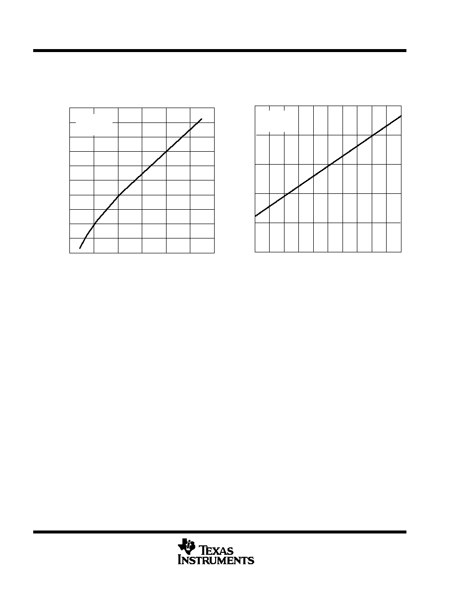
TYPICAL CHARACTERISTICS
Figure 4
PROPAGATION DELAY TIME
vs
LOAD CAPACITANCE
0
50
100
200
250
150
300
CL ≠ Load Capacitance ≠ pF
VCC = 5 V
TA = 25
∞
C
RL = 500
pd
t
≠
Propagation Delay T
ime ≠ ns
typ + 8
typ + 6
typ + 4
typ + 2
typ
typ ≠ 2
Figure 5
POWER-DISSIPATION CAPACITANCE
vs
SUPPLY VOLTAGE
C
pd
VCC ≠ Supply Voltage ≠ V
VCC = 5 V
fi = 5 MHz
TA = 25
∞
C
≠ Power Dissipation Capacitance ≠ pF
4.5
4.6
4.7
4.9
5
4.8
5.1
5.2
5.3
5.4
5.5
typ + 2
typ + 1
typ
typ ≠ 1
typ ≠ 2
typ ≠ 3

IMPORTANT NOTICE
Texas Instruments and its subsidiaries (TI) reserve the right to make changes to their products or to discontinue
any product or service without notice, and advise customers to obtain the latest version of relevant information
to verify, before placing orders, that information being relied on is current and complete. All products are sold
subject to the terms and conditions of sale supplied at the time of order acknowledgement, including those
pertaining to warranty, patent infringement, and limitation of liability.
TI warrants performance of its semiconductor products to the specifications applicable at the time of sale in
accordance with TI's standard warranty. Testing and other quality control techniques are utilized to the extent
TI deems necessary to support this warranty. Specific testing of all parameters of each device is not necessarily
performed, except those mandated by government requirements.
CERTAIN APPLICATIONS USING SEMICONDUCTOR PRODUCTS MAY INVOLVE POTENTIAL RISKS OF
DEATH, PERSONAL INJURY, OR SEVERE PROPERTY OR ENVIRONMENTAL DAMAGE ("CRITICAL
APPLICATIONS"). TI SEMICONDUCTOR PRODUCTS ARE NOT DESIGNED, AUTHORIZED, OR
WARRANTED TO BE SUITABLE FOR USE IN LIFE-SUPPORT DEVICES OR SYSTEMS OR OTHER
CRITICAL APPLICATIONS. INCLUSION OF TI PRODUCTS IN SUCH APPLICATIONS IS UNDERSTOOD TO
BE FULLY AT THE CUSTOMER'S RISK.
In order to minimize risks associated with the customer's applications, adequate design and operating
safeguards must be provided by the customer to minimize inherent or procedural hazards.
TI assumes no liability for applications assistance or customer product design. TI does not warrant or represent
that any license, either express or implied, is granted under any patent right, copyright, mask work right, or other
intellectual property right of TI covering or relating to any combination, machine, or process in which such
semiconductor products or services might be or are used. TI's publication of information regarding any third
party's products or services does not constitute TI's approval, warranty or endorsement thereof.
Copyright
©
1999, Texas Instruments Incorporated