
www.ti.com
FEATURES
PW PACKAGE
(TOP VIEW)
1
2
3
4
5
6
7
8
9
10
20
19
18
17
16
15
14
13
12
11
OE
1D
2D
3D
4D
5D
6D
7D
8D
GND
V
CC
1Q
2Q
3Q
4Q
5Q
6Q
7Q
8Q
LE
DESCRIPTION
SN74AHC573-Q1
OCTAL TRANSPARENT D-TYPE LATCH
WITH 3-STATE OUTPUTS
SCLS697 ≠ DECEMBER 2005
∑
Qualified for Automotive Applications
∑
Customer-Specific Configuration Control Can
Be Supported Along With Major-Change
Approval
∑
Operating Range 2-V to 5.5-V V
CC
∑
3-State Outputs Directly Drive Bus Lines
The SN74AHC573-Q1 is an octal transparent D-type latch designed for 2-V to 5.5-V V
CC
operation.
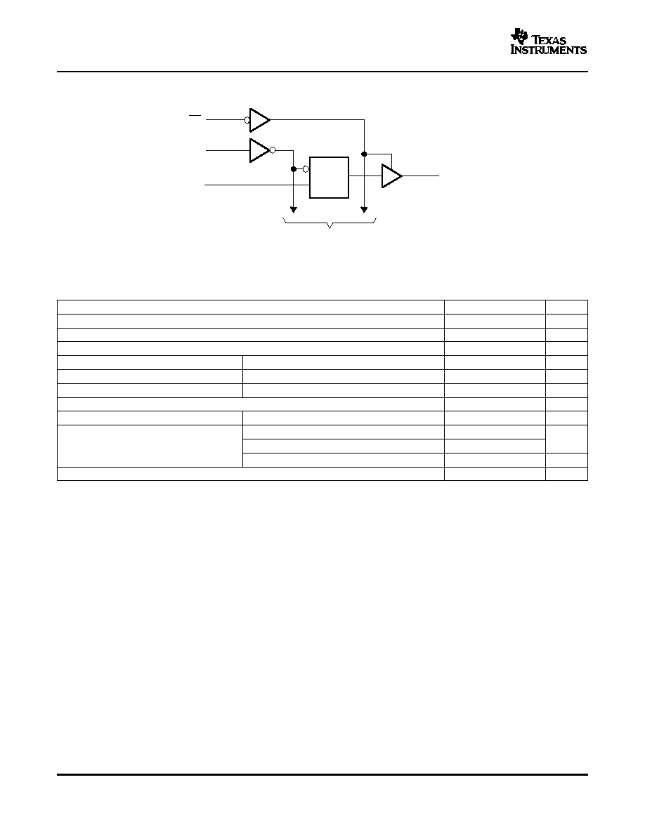
When the latch-enable (LE) input is high, the Q outputs follow the data (D) inputs. When LE is low, the Q outputs
are latched at the logic levels of the D inputs.
A buffered output-enable (OE) input can be used to place the eight outputs in either a normal logic state (high or
low) or the high-impedance state. In the high-impedance state, the outputs neither load nor drive the bus lines
significantly. The high-impedance state and increased drive provide the capability to drive bus lines without
interface or pullup components.
OE does not affect the internal operations of the latches. Old data can be retained or new data can be entered
while the outputs are in the high-impedance state.
To ensure the high-impedance state during power up or power down, OE should be tied to V
CC
through a pullup
resistor; the minimum value of the resistor is determined by the current-sinking capability of the driver.
ORDERING INFORMATION
T
A
PACKAGE
(1)
ORDERABLE PART NUMBER
TOP-SIDE MARKING
≠40
∞
C to 125
∞
C
TSSOP ≠ PW
Reel of 2000
SN74AHC573QPWRQ1
HA573Q
(1)
Package drawings, standard packing quantities, thermal data, symbolization, and PCB design guidelines are available at
www.ti.com/sc/package.
FUNCTION TABLE
(EACH LATCH)
INPUTS
OUTPUT
Q
OE
LE
D
L
H
H
H
L
H
L
L
L
L
X
Q
0
H
X
X
Z
Please be aware that an important notice concerning availability, standard warranty, and use in critical applications of Texas
Instruments semiconductor products and disclaimers thereto appears at the end of this data sheet.
PRODUCTION DATA information is current as of publication date.
Copyright © 2005, Texas Instruments Incorporated
Products conform to specifications per the terms of the Texas
Instruments standard warranty. Production processing does not
necessarily include testing of all parameters.
www.ti.com
OE
To Seven Other Channels
1
11
2
19
LE
1D
C1
1D
1Q
Absolute Maximum Ratings
(1)
SN74AHC573-Q1
OCTAL TRANSPARENT D-TYPE LATCH
WITH 3-STATE OUTPUTS
SCLS697 ≠ DECEMBER 2005
LOGIC DIAGRAM (POSITIVE LOGIC)
over operating free-air temperature range (unless otherwise noted)
MIN
MAX
UNIT
V
CC
Supply voltage range
≠0.5
7
V
V
I
Input voltage range
(2)
≠0.5
7
V
V
O
Output voltage range
(2)
≠0.5
V
CC
+ 0.5
V
I
IK
Input clamp current
V
I
< 0
≠20
mA
I
OK
Output clamp current
V
O
< 0 or V
O
> V
CC
±
20
mA
I
O
Continuous output current
V
O
= 0 to V
CC
±
25
mA
Continuous current through V
CC
or GND
±
75
mA
JA
Package thermal impedance
(3)
PW package
83
∞
C/W
Human-Body Model
1 (H1C)
kV
ESD rating
(4)
Charged-Device Model
1 (C5)
Machine Model
200 (M3)
V
T
stg
Storage temperature range
≠65
150
∞
C
(1)
Stresses beyond those listed under "absolute maximum ratings" may cause permanent damage to the device. These are stress ratings
only, and functional operation of the device at these or any other conditions beyond those indicated under "recommended operating
conditions" is not implied. Exposure to absolute-maximum-rated conditions for extended periods may affect device reliability.
(2)
The input and output voltage ratings may be exceeded if the input and output current ratings are observed.
(3)
The package thermal impedance is calculated in accordance with JESD 51-7.
(4)
ESD protection level per AEC Q100 classification
2

www.ti.com
Recommended Operating Conditions
(1)
Electrical Characteristics
SN74AHC573-Q1
OCTAL TRANSPARENT D-TYPE LATCH
WITH 3-STATE OUTPUTS
SCLS697 ≠ DECEMBER 2005
≠40
∞
C to 125
∞
C
≠40
∞
C to 85
∞
C
UNIT
MIN
MAX
MIN
MAX
V
CC
Supply voltage
2
5.5
2
5.5
V
V
CC
= 2 V
1.5
1.5
V
IH
High-level input voltage
V
CC
= 3 V
2.1
2.1
V
V
CC
= 5.5 V
3.85
3.85
V
CC
= 2 V
0.5
0.5
V
IL
Low-level input voltage
V
CC
= 3 V
0.9
0.9
V
V
CC
= 5.5 V
1.65
1.65
V
I
Input voltage
0
5.5
0
5.5
V
V
O
Output voltage
0
V
CC
0
V
CC
V
V
CC
= 2 V
≠50
≠50
µ
A
I
OH
High-level output current
V
CC
= 3.3 V
±
0.3 V
≠4
≠4
mA
V
CC
= 5 V
±
0.5 V
≠8
≠8
V
CC
= 2 V
50
50
µ
A
I
OL
Low-level output current
V
CC
= 3.3 V
±
0.3 V
4
4
mA
V
CC
= 5 V
±
0.5 V
8
8
V
CC
= 3.3 V
±
0.3 V
100
100
t/
v
Input transition rise or fall rate
ns/V
V
CC
= 5 V
±
0.5 V
20
20
T
A
Operating free-air temperature
≠40
125
≠40
85
∞
C
(1)
All unused inputs of the device must be held at V
CC
or GND to ensure proper device operation. Refer to the TI application report,
Implications of Slow or Floating CMOS Inputs, literature number SCBA004.
over recommended operating free-air temperature range (unless otherwise noted)
≠40
∞
C to
≠40
∞
C to
T
A
= 25
∞
C
125
∞
C
85
∞
C
PARAMETER
TEST CONDITIONS
V
CC
UNIT
MIN
TYP
MAX
MIN
MAX
MIN
MAX
2 V
1.9
2
1.9
1.9
I
OH
= ≠50
µ
A
3 V
2.9
3
2.9
2.9
V
OH
4.5 V
4.4
4.5
4.4
4.4
V
I
OH
= ≠4 mA
3 V
2.58
2.48
2.48
I
OH
= ≠8 mA
4.5 V
3.94
3.8
3.8
2 V
0.1
0.1
0.1
I
OL
= 50
µ
A
3 V
0.1
0.1
0.1
V
OL
4.5 V
0.1
0.1
0.1
V
I
OL
= 4 mA
3 V
0.36
0.5
0.44
I
OL
= 8 mA
4.5 V
0.36
0.5
0.44
I
I
V
I
= 5.5 V or GND
0 V to 5.5 V
±
0.1
±
1
±
1
µ
A
I
OZ
V
I
= V
IL
or V
IH
,
V
O
= V
CC
or GND
5.5 V
±
0.25
±
2.5
±
2.5
µ
A
I
CC
V
I
= V
CC
or GND,
I
O
= 0
5.5 V
4
40
40
µ
A
C
i
V
I
= V
CC
or GND
5 V
2.5
10
10
pF
C
o
V
O
= V
CC
or GND
5 V
3.5
pF
3

www.ti.com
Timing Requirements
Timing Requirements
Switching Characteristics
Switching Characteristics
Operating Characteristics
SN74AHC573-Q1
OCTAL TRANSPARENT D-TYPE LATCH
WITH 3-STATE OUTPUTS
SCLS697 ≠ DECEMBER 2005
over recommended operating free-air temperature range, V
CC
= 3.3 V
±
0.3 V (unless otherwise noted) (see
Figure 1
)
T
A
= 25
∞
C
≠40
∞
C to 125
∞
C
≠40
∞
C to 85
∞
C
UNIT
MIN
MAX
MIN
MAX
MIN
MAX
t
w
Pulse duration, LE high
5
5
5
ns
t
su
Setup time, data before LE
3.5
3.5
3.5
ns
t
h
Hold time, data after LE
1.5
1.5
1.5
ns
over recommended operating free-air temperature range, V
CC
= 5 V
±
0.5 V (unless otherwise noted) (see
Figure 1
)
T
A
= 25
∞
C
≠40
∞
C to 125
∞
C
≠40
∞
C to 85
∞
C
UNIT
MIN
MAX
MIN
MAX
MIN
MAX
t
w
Pulse duration, LE high
5
5
5
ns
t
su
Setup time, data before LE
3.5
3.5
3.5
ns
t
h
Hold time, data after LE
1.5
1.5
1.5
ns
over recommended operating free-air temperature range, V
CC
= 3.3 V
±
0.3 V (unless otherwise noted) (see
Figure 1
)
≠40
∞
C to
≠40
∞
C to
T
A
= 25
∞
C
FROM
TO
LOAD
125
∞
C
85
∞
C
PARAMETER
UNIT
(INPUT)
(OUTPUT)
CAPACITANCE
MIN
TYP
MAX
MIN
MAX
MIN
MAX
t
PLH
9.5
14.5
1
16.5
1
16.5
D
Q
C
L
= 50 pF
ns
t
PHL
9.5
14.5
1
16.5
1
16.5
t
PLH
10.1
15.4
1
17.5
1
17.5
LE
Q
C
L
= 50 pF
ns
t
PHL
10.1
15.4
1
17.5
1
17.5
t
PZH
9.8
15
1
17
1
17
OE
Q
C
L
= 50 pF
ns
t
PZL
9.8
15
1
17
1
17
t
PHZ
10.7
14.5
1
16.5
1
16.5
OE
Q
C
L
= 50 pF
ns
t
PLZ
10.7
14.5
1
16.5
1
16.5
over recommended operating free-air temperature range, V
CC
= 5 V
±
0.5 V (unless otherwise noted) (see
Figure 1
)
≠40
∞
C to
≠40
∞
C to
T
A
= 25
∞
C
FROM
TO
LOAD
125
∞
C
85
∞
C
PARAMETER
UNIT
(INPUT)
(OUTPUT)
CAPACITANCE
MIN
TYP
MAX
MIN
MAX
MIN
MAX
t
PLH
6
8.8
1
10
1
10
D
Q
C
L
= 50 pF
ns
t
PHL
6
8.8
1
10
1
10
t
PLH
6.5
9.7
1
11
1
11
LE
Q
C
L
= 50 pF
ns
t
PHL
6.5
9.7
1
11
1
11
t
PZH
6.7
9.7
1
11
1
11
OE
Q
C
L
= 50 pF
ns
t
PZL
6.7
9.7
1
11
1
11
t
PHZ
6.7
9.7
1
11
1
11
OE
Q
C
L
= 50 pF
ns
t
PLZ
6.7
9.7
1
11
1
11
V
CC
= 5 V, T
A
= 25
∞
C
PARAMETER
TEST CONDITIONS
TYP
UNIT
C
pd
Power dissipation capacitance
No load,
f = 1 MHz
16
pF
4
www.ti.com
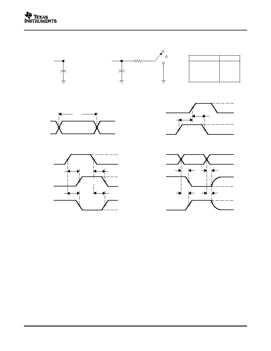
PARAMETER MEASUREMENT INFORMATION
50% V
CC
V
CC
V
CC
0 V
0 V
t
h
t
su
VOLTAGE WAVEFORMS
SETUP AND HOLD TIMES
Data Input
t
PLH
t
PHL
t
PHL
t
PLH
V
OH
V
OH
V
OL
V
OL
V
CC
0 V
50% V
CC
50% V
CC
Input
Out-of-Phase
Output
In-Phase
Output
Timing Input
50% V
CC
VOLTAGE WAVEFORMS
PROPAGATION DELAY TIMES
INVERTING AND NONINVERTING OUTPUTS
Output
Control
Output
Waveform 1
S1 at V
CC
(see Note B)
Output
Waveform 2
S1 at GND
(see Note B)
V
OL
V
OH
t
PZL
t
PZH
t
PLZ
t
PHZ
V
CC
0 V
50% V
CC
V
OL
+ 0.3 V
50% V
CC
0 V
V
CC
VOLTAGE WAVEFORMS
ENABLE AND DISABLE TIMES
LOW- AND HIGH-LEVEL ENABLING
t
PLH
/t
PHL
t
PLZ
/t
PZL
t
PHZ
/t
PZH
Open Drain
Open
V
CC
GND
V
CC
TEST
S1
V
CC
0 V
50% V
CC
t
w
VOLTAGE WAVEFORMS
PULSE DURATION
Input
NOTES: A. C
L
includes probe and jig capacitance.
B. Waveform 1 is for an output with internal conditions such that the output is low, except when disabled by the output control.
Waveform 2 is for an output with internal conditions such that the output is high, except when disabled by the output control.
C. All input pulses are supplied by generators having the following characteristics: PRR
1 MHz, Z
O
= 50
, t
r
3 ns, t
f
3 ns.
D. The outputs are measured one at a time, with one input transition per measurement.
E. All parameters and waveforms are not applicable to all devices.
From Output
Under Test
C
L
(see Note A)
LOAD CIRCUIT FOR
3-STATE AND OPEN-DRAIN OUTPUTS
S1
V
CC
R
L
= 1 k
GND
From Output
Under Test
C
L
(see Note A)
Test
Point
LOAD CIRCUIT FOR
TOTEM-POLE OUTPUTS
Open
50% V
CC
50% V
CC
50% V
CC
50% V
CC
50% V
CC
50% V
CC
50% V
CC
50% V
CC
V
OH
-
0.3 V
SN74AHC573-Q1
OCTAL TRANSPARENT D-TYPE LATCH
WITH 3-STATE OUTPUTS
SCLS697 ≠ DECEMBER 2005
Figure 1. Load Circuits and Voltage Waveforms
5