SN74AHCT00-EP
QUADRUPLE 2-INPUT POSITIVE-NAND GATES
SCLS507 ≠ JUNE 2003
1
POST OFFICE BOX 655303
∑
DALLAS, TEXAS 75265
D
Controlled Baseline
≠ One Assembly/Test Site, One Fabrication
Site
D
Extended Temperature Performance of
≠55
į
C to 125
į
C
D
Enhanced Diminishing Manufacturing
Sources (DMS) Support
D
Enhanced Product-Change Notification
D
Qualification Pedigree
D
Inputs Are TTL-Voltage Compatible
Component qualification in accordance with JEDEC and industry
standards to ensure reliable operation over an extended
temperature range. This includes, but is not limited to, Highly
Accelerated Stress Test (HAST) or biased 85/85, temperature
cycle, autoclave or unbiased HAST, electromigration, bond
intermetallic life, and mold compound life. Such qualification testing
should not be viewed as justifying use of this component beyond
specified performance and environmental limits.
D
Latch-Up Performance Exceeds 250 mA Per
JESD 17
D
ESD Protection Exceeds JESD 22
≠ 2000-V Human-Body Model (A114-A)
≠ 200-V Machine Model (A115-A)
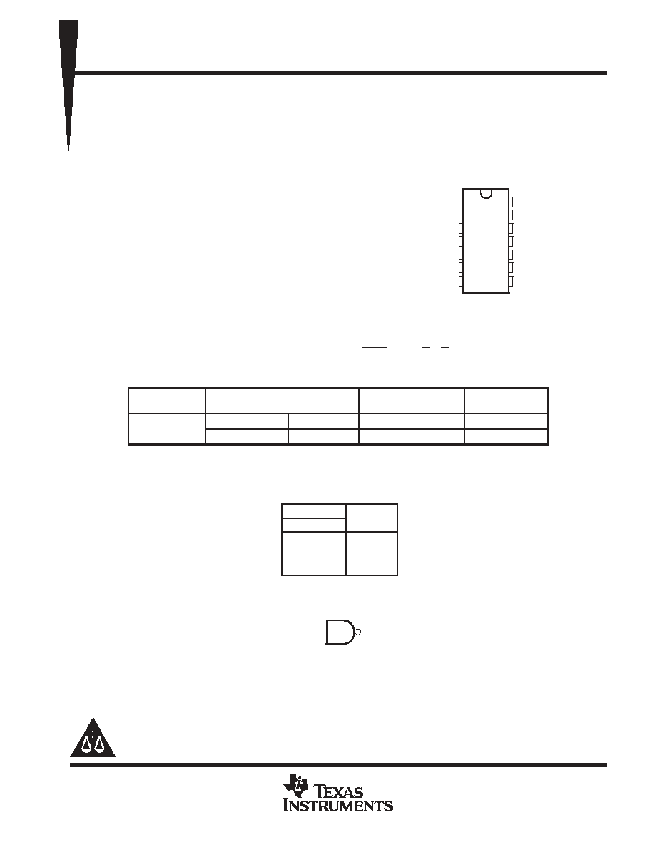
description/ordering information
The 'AHCT00 device performs the Boolean function Y = A
∑
B or Y = A + B in positive logic.
ORDERING INFORMATION
TA
PACKAGE
ORDERABLE
PART NUMBER
TOP-SIDE
MARKING
≠55
į
C to 125
į
C
SOIC ≠ D
Tape and reel
SN74AHCT00MDREP
AHCT00MEP
≠55
į
C to 125
į
C
TSSOP ≠ PW
Tape and reel
SN74AHCT00MPWREP
AHT00EP
Package drawings, standard packing quantities, thermal data, symbolization, and PCB design guidelines
are available at www.ti.com/sc/package.
FUNCTION TABLE
(each gate)
INPUTS
OUTPUT
Y
A
B
OUTPUT
Y
H
H
L
L
X
H
X
L
H
logic diagram, each gate (positive logic)
A
B
Y
1
2
3
4
5
6
7
14
13
12
11
10
9
8
1A
1B
1Y
2A
2B
2Y
GND
V
CC
4B
4A
4Y
3B
3A
3Y
D OR PW PACKAGE
(TOP VIEW)
PRODUCTION DATA information is current as of publication date.
Products conform to specifications per the terms of Texas Instruments
standard warranty. Production processing does not necessarily include
testing of all parameters.
Copyright
2003, Texas Instruments Incorporated
Please be aware that an important notice concerning availability, standard warranty, and use in critical applications of
Texas Instruments semiconductor products and disclaimers thereto appears at the end of this data sheet.

SN74AHCT00-EP
QUADRUPLE 2-INPUT POSITIVE-NAND GATES
SCLS507 ≠ JUNE 2003
2
POST OFFICE BOX 655303
∑
DALLAS, TEXAS 75265
absolute maximum ratings over operating free-air temperature range (unless otherwise noted)
Supply voltage range, V
CC
≠0.5 V to 7 V
. . . . . . . . . . . . . . . . . . . . . . . . . . . . . . . . . . . . . . . . . . . . . . . . . . . . . . . . . .
Input voltage range, V
I
(see Note 1)
≠0.5 V to 7 V
. . . . . . . . . . . . . . . . . . . . . . . . . . . . . . . . . . . . . . . . . . . . . . . . . .
Output voltage range, V
O
(see Note 1)
≠0.5 V to V
CC
+ 0.5 V
. . . . . . . . . . . . . . . . . . . . . . . . . . . . . . . . . . . . . . . .
Input clamp current, I
IK
(V
I
< 0)
≠20 mA
. . . . . . . . . . . . . . . . . . . . . . . . . . . . . . . . . . . . . . . . . . . . . . . . . . . . . . . . . . .
Output clamp current, I
OK
(V
O
< 0 or V
O
> V
CC
)
Ī
20 mA
. . . . . . . . . . . . . . . . . . . . . . . . . . . . . . . . . . . . . . . . . . . .
Continuous output current, I
O
(V
O
= 0 to V
CC
)
Ī
25 mA
. . . . . . . . . . . . . . . . . . . . . . . . . . . . . . . . . . . . . . . . . . . . . .
Continuous current through V
CC
or GND
Ī
50 mA
. . . . . . . . . . . . . . . . . . . . . . . . . . . . . . . . . . . . . . . . . . . . . . . . . . .
Package thermal impedance,
JA
(see Note 2): D package
86
į
C/W
. . . . . . . . . . . . . . . . . . . . . . . . . . . . . . . . . . .
PW package
113
į
C/W
. . . . . . . . . . . . . . . . . . . . . . . . . . . . . . . .
Storage temperature range, T
stg
≠65
į
C to 150
į
C
. . . . . . . . . . . . . . . . . . . . . . . . . . . . . . . . . . . . . . . . . . . . . . . . . . .
Stresses beyond those listed under "absolute maximum ratings" may cause permanent damage to the device. These are stress ratings only, and
functional operation of the device at these or any other conditions beyond those indicated under "recommended operating conditions" is not
implied. Exposure to absolute-maximum-rated conditions for extended periods may affect device reliability.
NOTES:
1. The input and output voltage ratings may be exceeded if the input and output current ratings are observed.
2. The package thermal impedance is calculated in accordance with JESD 51-7.
recommended operating conditions (see Note 3)
MIN
MAX
UNIT
VCC
Supply voltage
4.5
5.5
V
VIH
High-level input voltage
2
V
VIL
Low-level input voltage
0.8
V
VI
Input voltage
0
5.5
V
VO
Output voltage
0
VCC
V
IOH
High-level output current
≠8
mA
IOL
Low-level output current
8
mA
t/
v
Input transition rise or fall rate
20
ns/V
TA
Operating free-air temperature
≠55
125
į
C
NOTE 3: All unused inputs of the device must be held at VCC or GND to ensure proper device operation. Refer to the TI application report,
Implications of Slow or Floating CMOS Inputs, literature number SCBA004.
electrical characteristics over recommended operating free-air temperature range (unless
otherwise noted)
PARAMETER
TEST CONDITIONS
VCC
TA = 25
į
C
SN74AHCT00-EP
UNIT
PARAMETER
TEST CONDITIONS
VCC
MIN
TYP
MAX
MIN
MAX
UNIT
VOH
IOH = ≠50
m
A
4.5 V
4.4
4.5
4.4
V
VOH
IOH = ≠8 mA
4.5 V
3.94
3.8
V
VOL
IOL = 50
m
A
4.5 V
0.1
0.1
V
VOL
IOL = 8 mA
4.5 V
0.36
0.44
V
II
VI = 5.5 V or GND
0 V to 5.5 V
Ī
0.1
Ī
1
m
A
ICC
VI = VCC or GND,
IO = 0
5.5 V
2
20
m
A
ICC
One input at 3.4 V,
Other inputs at VCC or GND
5.5 V
1.35
1.5
mA
Ci
VI = VCC or GND
5 V
2
10
pF
This is the increase in supply current for each input at one of the specified TTL voltage levels, rather than 0 V or VCC.

SN74AHCT00-EP
QUADRUPLE 2-INPUT POSITIVE-NAND GATES
SCLS507 ≠ JUNE 2003
3
POST OFFICE BOX 655303
∑
DALLAS, TEXAS 75265
switching characteristics over recommended operating free-air temperature range,
V
CC
= 5 V
Ī
0.5 V (unless otherwise noted) (see Figure 1)
PARAMETER
FROM
TO
LOAD
TA = 25
į
C
SN74AHCT00-EP
UNIT
PARAMETER
FROM
(INPUT)
TO
(OUTPUT)
LOAD
CAPACITANCE
MIN
TYP
MAX
MIN
MAX
UNIT
tPLH
A or B
Y
CL = 15 pF
5
6.9
1
8
ns
tPHL
A or B
Y
CL = 15 pF
5
6.9
1
8
ns
tPLH
A or B
Y
CL = 50 pF
5.5
7.9
1
9
ns
tPHL
A or B
Y
CL = 50 pF
5.5
7.9
1
9
ns
noise characteristics, V
CC
= 5 V, C
L
= 50 pF, T
A
= 25
į
C (see Note 4)
PARAMETER
MIN
TYP
MAX
UNIT
VOL(P)
Quiet output, maximum dynamic VOL
0.4
0.8
V
VOL(V)
Quiet output, minimum dynamic VOL
≠0.4
≠0.8
V
VOH(V)
Quiet output, minimum dynamic VOH
4.5
V
VIH(D)
High-level dynamic input voltage
2
V
VIL(D)
Low-level dynamic input voltage
0.8
V
NOTE 4: Characteristics are for surface-mount packages only.
operating characteristics, V
CC
= 5 V, T
A
= 25
į
C
PARAMETER
TEST CONDITIONS
TYP
UNIT
Cpd
Power dissipation capacitance
No load,
f = 1 MHz
10.5
pF
SN74AHCT00-EP
QUADRUPLE 2-INPUT POSITIVE-NAND GATES
SCLS507 ≠ JUNE 2003
4
POST OFFICE BOX 655303
∑
DALLAS, TEXAS 75265
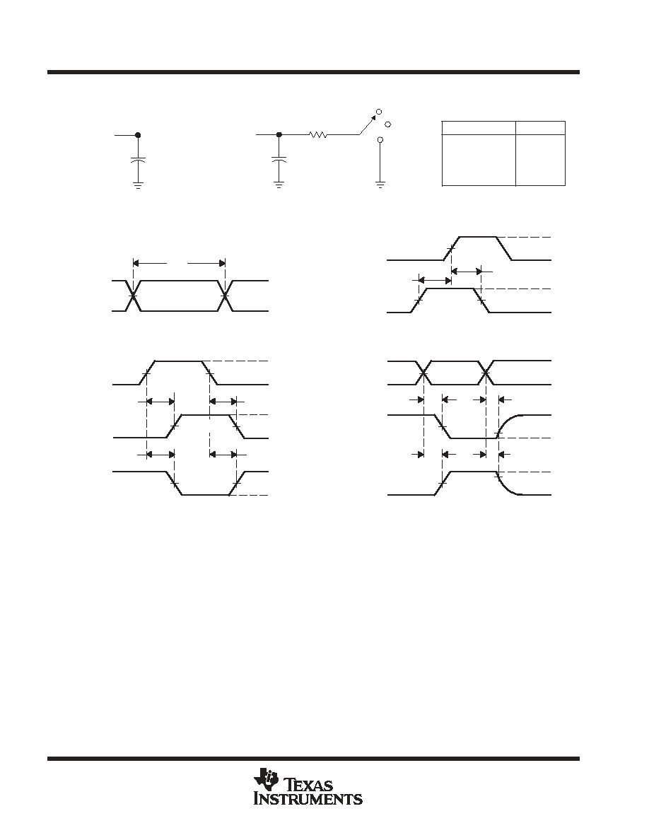
PARAMETER MEASUREMENT INFORMATION
50% VCC
3 V
3 V
0 V
0 V
th
tsu
VOLTAGE WAVEFORMS
SETUP AND HOLD TIMES
Data Input
tPLH
tPHL
tPHL
tPLH
VOH
VOH
VOL
VOL
3 V
0 V
50% VCC
50% VCC
Input
Out-of-Phase
Output
In-Phase
Output
Timing Input
50% VCC
VOLTAGE WAVEFORMS
PROPAGATION DELAY TIMES
INVERTING AND NONINVERTING OUTPUTS
Output
Control
Output
Waveform 1
S1 at VCC
(see Note B)
Output
Waveform 2
S1 at GND
(see Note B)
VOL
VOH
tPZL
tPZH
tPLZ
tPHZ
VCC
0 V
50% VCC
VOL
+ 0.3 V
50% VCC
0 V
3 V
VOLTAGE WAVEFORMS
ENABLE AND DISABLE TIMES
LOW- AND HIGH-LEVEL ENABLING
tPLH/tPHL
tPLZ/tPZL
tPHZ/tPZH
Open Drain
Open
VCC
GND
VCC
TEST
S1
3 V
0 V
tw
VOLTAGE WAVEFORMS
PULSE DURATION
Input
NOTES: A. CL includes probe and jig capacitance.
B. Waveform 1 is for an output with internal conditions such that the output is low except when disabled by the output control.
Waveform 2 is for an output with internal conditions such that the output is high except when disabled by the output control.
C. All input pulses are supplied by generators having the following characteristics: PRR
1 MHz, ZO = 50
, tr
3 ns, tf
3 ns.
D. The outputs are measured one at a time with one input transition per measurement.
E. All parameters and waveforms are not applicable to all devices.
From Output
Under Test
CL
(see Note A)
LOAD CIRCUIT FOR
3-STATE AND OPEN-DRAIN OUTPUTS
S1
VCC
RL = 1 k
GND
From Output
Under Test
CL
(see Note A)
Test
Point
LOAD CIRCUIT FOR
TOTEM-POLE OUTPUTS
Open
VOH ≠
0.3 V
1.5 V
1.5 V
1.5 V
1.5 V
1.5 V
1.5 V
1.5 V
1.5 V
1.5 V
Figure 1. Load Circuit and Voltage Waveforms
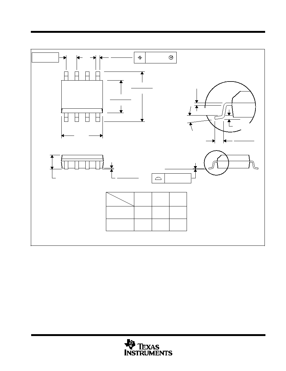
MECHANICAL DATA
MSOI002B ≠ JANUARY 1995 ≠ REVISED SEPTEMBER 2001
1
POST OFFICE BOX 655303
∑
DALLAS, TEXAS 75265
D (R-PDSO-G**)
PLASTIC SMALL-OUTLINE PACKAGE
8 PINS SHOWN
8
0.197
(5,00)
A MAX
A MIN
(4,80)
0.189
0.337
(8,55)
(8,75)
0.344
14
0.386
(9,80)
(10,00)
0.394
16
DIM
PINS **
4040047/E 09/01
0.069 (1,75) MAX
Seating Plane
0.004 (0,10)
0.010 (0,25)
0.010 (0,25)
0.016 (0,40)
0.044 (1,12)
0.244 (6,20)
0.228 (5,80)
0.020 (0,51)
0.014 (0,35)
1
4
8
5
0.150 (3,81)
0.157 (4,00)
0.008 (0,20) NOM
0
į
≠ 8
į
Gage Plane
A
0.004 (0,10)
0.010 (0,25)
0.050 (1,27)
NOTES: A. All linear dimensions are in inches (millimeters).
B. This drawing is subject to change without notice.
C. Body dimensions do not include mold flash or protrusion, not to exceed 0.006 (0,15).
D. Falls within JEDEC MS-012