
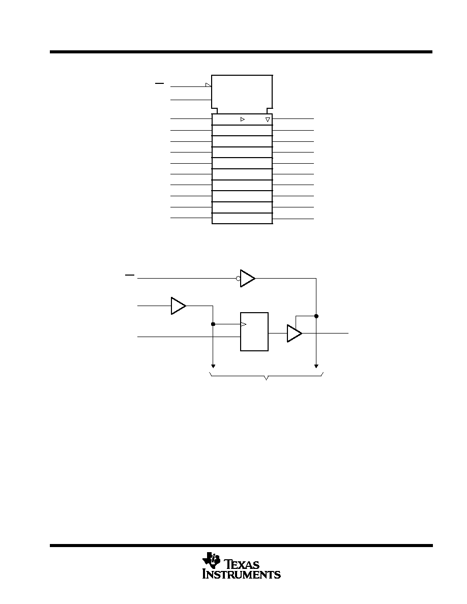
DW OR NT PACKAGE
(TOP VIEW)
1
2
3
4
5
6
7
8
9
10
11
12
24
23
22
21
20
19
18
17
16
15
14
13
OE
1D
2D
3D
4D
5D
6D
7D
8D
9D
10D
GND
V
CC
1Q
2Q
3Q
4Q
5Q
6Q
7Q
8Q
9Q
10Q
LE
SN74ALS29841
10-BIT BUS-INTERFACE D-TYPE LATCH
WITH 3-STATE OUTPUTS
SDAS149A � JUNE 1988 � REVISED JANUARY 1995
Copyright
�
1995, Texas Instruments Incorporated
1
POST OFFICE BOX 655303
�
DALLAS, TEXAS 75265
�
3-State Buffer-Type Outputs Drive Bus
Lines Directly
�
Bus-Structured Pinout
�
Provides Extra Bus-Driving Latches
Necessary for Wider Address/Data Paths or
Buses With Parity
�
Buffered Control Inputs Reduce dc Loading
Effects
�
Power-Up High-Impedance State
�
Package Options Include Plastic
Small-Outline (DW) Packages and Standard
Plastic (NT) 300-mil DIPs
description
This 10-bit latch features 3-state outputs designed
specifically for driving highly capacitive or relatively low-impedance loads. It is particularly suitable for
implementing buffer registers, I/O ports, bidirectional bus drivers, and working registers.
The ten latches are transparent D-type latches. The SN74ALS29841 has noninverting data (D) inputs.
A buffered output-enable (OE) input can place the ten outputs in either a normal logic state (high or low logic
levels) or in a high-impedance state. The outputs also are in the high-impedance state during power-up and
power-down conditions. The outputs remain in the high-impedance state while the device is powered down. In
the high-impedance state, the outputs neither load nor drive the bus lines significantly. The high-impedance
state and increased drive provide the capability to drive bus lines without interface or pullup components.
OE does not affect the internal operation of the latches. Old data can be retained or new data can be entered
while the outputs are off.
The SN74ALS29841 is characterized for operation from 0
�
C to 70
�
C.
FUNCTION TABLE
INPUTS
OUTPUT
OE
LE
D
Q
L
H
H
H
L
H
L
L
L
L
X
Q0
H
X
X
Z
PRODUCTION DATA information is current as of publication date.
Products conform to specifications per the terms of Texas Instruments
standard warranty. Production processing does not necessarily include
testing of all parameters.
SN74ALS29841
10-BIT BUS-INTERFACE D-TYPE LATCH
WITH 3-STATE OUTPUTS
SDAS149A � JUNE 1988 � REVISED JANUARY 1995
2
POST OFFICE BOX 655303
�
DALLAS, TEXAS 75265
logic symbol
EN
1
7
6D
8
7D
9
8D
10
9D
1D
2
1D
6Q
18
7Q
17
8Q
16
9Q
15
1Q
23
3
2D
4
3D
5
4D
6
5D
2Q
22
3Q
21
4Q
20
5Q
19
OE
C1
13
LE
11
10D
10Q
14
This symbol is in accordance with ANSI/IEEE Std 91-1984 and IEC Publication 617-12.
logic diagram (positive logic)
1D
OE
2
1
13
1Q
23
LE
1D
To Nine Other Channels
C1
absolute maximum ratings over operating free-air temperature range (unless otherwise noted)
Supply voltage, V
CC
7 V
. . . . . . . . . . . . . . . . . . . . . . . . . . . . . . . . . . . . . . . . . . . . . . . . . . . . . . . . . . . . . . . . . . . . . . . .
Input voltage, V
I
7 V
. . . . . . . . . . . . . . . . . . . . . . . . . . . . . . . . . . . . . . . . . . . . . . . . . . . . . . . . . . . . . . . . . . . . . . . . . . . .
Voltage applied to a disabled 3-state output
5.5 V
. . . . . . . . . . . . . . . . . . . . . . . . . . . . . . . . . . . . . . . . . . . . . . . . . .
Operating free-air temperature range, T
A
0
�
C to 70
�
C
. . . . . . . . . . . . . . . . . . . . . . . . . . . . . . . . . . . . . . . . . . . . . .
Storage temperature range
� 65
�
C to 150
�
C
. . . . . . . . . . . . . . . . . . . . . . . . . . . . . . . . . . . . . . . . . . . . . . . . . . . . . . .
Stresses beyond those listed under "absolute maximum ratings" may cause permanent damage to the device. These are stress ratings only, and
functional operation of the device at these or any other conditions beyond those indicated under "recommended operating conditions" is not
implied. Exposure to absolute-maximum-rated conditions for extended periods may affect device reliability.

SN74ALS29841
10-BIT BUS-INTERFACE D-TYPE LATCH
WITH 3-STATE OUTPUTS
SDAS149A � JUNE 1988 � REVISED JANUARY 1995
3
POST OFFICE BOX 655303
�
DALLAS, TEXAS 75265
recommended operating conditions
MIN
NOM
MAX
UNIT
VCC
Supply voltage
4.75
5
5.25
V
VIH
High-level input voltage
2
V
VIL
Low-level input voltage
0.8
V
IOH
High-level output current
� 24
mA
IOL
Low-level output current
48
mA
tw
Pulse duration, LE high
6
ns
tsu
Setup time, data before LE
2.5
ns
th
Hold time, data after LE
4.5
ns
TA
Operating free-air temperature
0
70
�
C
electrical characteristics over recommended operating free-air temperature range (unless
otherwise noted)
PARAMETER
TEST CONDITIONS
MIN
TYP
MAX
UNIT
VIK
VCC = 4.75 V,
II = � 18 mA
� 1.2
V
VOH
VCC = 4 75 V
IOH = � 15 mA
2.4
3.3
V
VOH
VCC = 4.75 V
IOH = � 24 mA
2
3.1
V
VOL
VCC = 4.75 V,
IOL = 48 mA
0.35
0.5
V
IOZH
VCC = 5.25 V,
VO = 2.7 V
20
�
A
IOZL
VCC = 5.25 V,
VO = 0.4 V
� 20
�
A
II
VCC = 5.25 V,
VI = 5.5 V
0.1
mA
IIH
VCC = 5.25 V,
VI = 2.7 V
20
�
A
IIL
VCC = 5.25 V,
VI = 0.4 V
� 0.2
mA
IOS
VCC = 5.25 V,
VO = 0
� 75
� 250
mA
ICC
VCC = 5.25 V,
Outputs low
55
85
mA
All typical values are at VCC = 5 V, TA = 25
�
C.
Not more than one output should be shorted at a time, and the duration of the short circuit should not exceed one second.

SN74ALS29841
10-BIT BUS-INTERFACE D-TYPE LATCH
WITH 3-STATE OUTPUTS
SDAS149A � JUNE 1988 � REVISED JANUARY 1995
4
POST OFFICE BOX 655303
�
DALLAS, TEXAS 75265
switching characteristics (see Figure 1)
PARAMETER
FROM
(INPUT)
TO
(OUTPUT)
TEST CONDITIONS
VCC = MIN to MAX,
TA = MIN to MAX
UNIT
(INPUT)
(OUTPUT)
MIN
MAX
tPLH
D
An Q
C
50 pF
2
9.5
ns
tPHL
D
Any Q
CL = 50 pF
2
9.5
ns
tPLH
D
An Q
C
300 pF
14
ns
tPHL
D
Any Q
CL = 300 pF
14
ns
tPLH
LE
An Q
C
50 pF
12
ns
tPHL
LE
Any Q
CL = 50 pF
12
ns
tPLH
LE
An Q
C
300 pF
16
ns
tPHL
LE
Any Q
CL = 300 pF
16
ns
tPZH
OE
An Q
C
50 pF
14
ns
tPZL
OE
Any Q
CL = 50 pF
14
ns
tPZH
OE
An Q
C
300 pF
20
ns
tPZL
OE
Any Q
CL = 300 pF
23
ns
tPHZ
OE
An Q
C
50 pF
15
ns
tPLZ
OE
Any Q
CL = 50 pF
12
ns
tPHZ
OE
Any Q
CL 5 pF
9
ns
tPLZ
OE
Any Q
CL = 5 pF
9
ns
For conditions shown as MIN or MAX, use the appropriate value specified under recommended operating conditions.
SN74ALS29841
10-BIT BUS-INTERFACE D-TYPE LATCH
WITH 3-STATE OUTPUTS
SDAS149A � JUNE 1988 � REVISED JANUARY 1995
5
POST OFFICE BOX 655303
�
DALLAS, TEXAS 75265
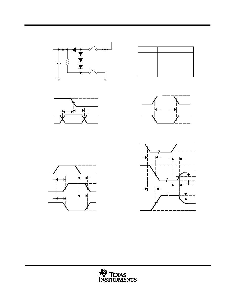
PARAMETER MEASUREMENT INFORMATION
LOAD CIRCUIT
R1
1 k
All Diodes
1N916 or 1N3064
From Output
Under Test
Test Point
S2
CL
(see Note A)
RL = 180
1.5 V
1.5 V
1.5 V
3 V
3 V
0
0
th
tsu
VOLTAGE WAVEFORMS
SETUP AND HOLD TIMES
Timing Input
Data Input
1.5 V
1.5 V
3 V
3 V
0
0
High-Level
Pulse
Low-Level
Pulse
tw
VOLTAGE WAVEFORMS
PULSE DURATIONS
1.5 V
1.5 V
tPHL
tPLH
tPLH
tPHL
Out-of-Phase
Output
1.5 V
1.5 V
1.5 V
1.5 V
1.5 V
1.5 V
3 V
0
VOL
VOH
VOH
VOL
In-Phase
Output
VOLTAGE WAVEFORMS
PROPAGATION DELAY TIMES
tPHZ
tPLZ
0.5 V
tPZL
tPZH
1.5 V
1.5 V
1.5 V
1.5 V
3 V
0
Output
Control
Waveform 1
(see Note B)
Waveform 2
(see Note B)
0
VOH
VOL
1.5 V
0.5 V
VOLTAGE WAVEFORMS
ENABLE AND DISABLE TIMES, 3-STATE OUTPUTS
VCC
S1
SWITCH POSITION TABLE
TEST
S1
S2
tPLH
tPHL
tPZH
tPZL
tPHZ
tPLZ
Closed
Closed
Open
Closed
Closed
Closed
Closed
Closed
Closed
Open
Closed
Closed
4.5 V
1.5 V
Input
NOTES: A. CL includes probe and jig capacitance.
B. Waveform 1 is for an output with internal conditions such that the output is low except when disabled by the output control.
Waveform 2 is for an output with internal conditions such that the output is high except when disabled by the output control.
C. All input pulses are supplied by generators having the following characteristics: PRR
10 MHz, ZO = 50
,
tr
2.5 ns, tf
2.5 ns.
Figure 1. Load Circuit and Voltage Waveforms