
SN54ALS652, SN54ALS653, SN54AS651, SN54AS652
SN74ALS651A, SN74ALS652A, SN74ALS653, SN74ALS654, SN74AS651, SN74AS652
OCTAL BUS TRANSCEIVERS AND REGISTERS WITH 3-STATE OUTPUTS
SDAS066F ≠ DECEMBER 1983 ≠ REVISED OCTOBER 1996
1
POST OFFICE BOX 655303
∑
DALLAS, TEXAS 75265
D
Bus Transceivers/Registers
D
Independent Registers and Enables for A
and B Buses
D
Multiplexed Real-Time and Stored Data
D
Choice of True or Inverting Data Paths
D
Choice of 3-State or Open-Collector
Outputs to A Bus
D
Package Options Include Plastic
Small-Outline (DW) Packages, Ceramic
Chip Carriers (FK), and Standard Plastic
(NT) and Ceramic (JT) 300-mil DIPs
DEVICE
A OUTPUT
B OUTPUT
LOGIC
SN74ALS651A,
'AS651
3 State
3 State
Inverting
SN54ALS652,
SN74ALS652A,
'AS652
3 State
3 State
True
'ALS653
Open Collector
3 State
Inverting
SN74ALS654
Open Collector
3 State
True
description
These devices consist of bus-transceiver circuits,
D-type flip-flops, and control circuitry arranged for
multiplexed transmission of data directly from the
data bus or from the internal storage registers.
Output-enable (OEAB and OEBA) inputs are
provided to control the transceiver functions.
Select-control (SAB and SBA) inputs are provided
to select real-time or stored data transfer. The
circuitry used for select control eliminates the
typical decoding glitch that occurs in a multiplexer
during the transition between stored and real-time
data. A low input level selects real-time data, and
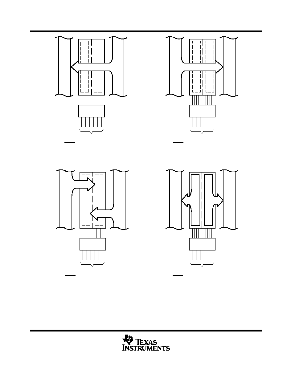
a high input level selects stored data. Figure 1
illustrates the four fundamental bus-management functions that can be performed with the octal bus
transceivers and registers.
Data on the A or B data bus, or both, can be stored in the internal D-type flip-flops by low-to-high transitions at
the appropriate clock (CLKAB or CLKBA) terminals, regardless of the select- or output-control terminals. When
SAB and SBA are in the real-time transfer mode, it is possible to store data without using the internal D-type
flip-flops by simultaneously enabling OEAB and OEBA. In this configuration, each output reinforces its input.
When all other data sources to the two sets of bus lines are at high impedance, each set of bus lines remains
at its last state.
Copyright
©
1996, Texas Instruments Incorporated
PRODUCTION DATA information is current as of publication date.
Products conform to specifications per the terms of Texas Instruments
standard warranty. Production processing does not necessarily include
testing of all parameters.
Please be aware that an important notice concerning availability, standard warranty, and use in critical applications of
Texas Instruments semiconductor products and disclaimers thereto appears at the end of this data sheet.
NC ≠ No internal connection
SN54ALS', SN54AS' . . . FK PACKAGE
(TOP VIEW)
SN54ALS', SN54AS' . . . JT PACKAGE
SN74ALS', SN74AS' . . . DW OR NT PACKAGE
(TOP VIEW)
1
2
3
4
5
6
7
8
9
10
11
12
24
23
22
21
20
19
18
17
16
15
14
13
CLKAB
SAB
OEAB
A1
A2
A3
A4
A5
A6
A7
A8
GND
V
CC
CLKBA
SBA
OEBA
B1
B2
B3
B4
B5
B6
B7
B8
3 2 1
13 14
5
6
7
8
9
10
11
OEBA
B1
B2
NC
B3
B4
B5
A1
A2
A3
NC
A4
A5
A6
4
15 16 17 18
A8
GND
NC
B8
B7
B6
OEAB
SAB
CLKAB
NC
28 27 26
25
24
23
22
21
20
19
12
A7
CLKBA
SAB
CC
V

SN54ALS652, SN54ALS653, SN54AS651, SN54AS652
SN74ALS651A, SN74ALS652A, SN74ALS653, SN74ALS654, SN74AS651, SN74AS652
OCTAL BUS TRANSCEIVERS AND REGISTERS WITH 3-STATE OUTPUTS
SDAS066F ≠ DECEMBER 1983 ≠ REVISED OCTOBER 1996
2
POST OFFICE BOX 655303
∑
DALLAS, TEXAS 75265
description (continued)
The -1 versions of the SN74ALS651A and SN74ALS652A are identical to the standard versions except that the
recommended maximum I
OL
for the -1 versions is increased to 48 mA. There are no -1 versions of the
SN54ALS652, SN54ALS653, SN74ALS653, and SN74ALS654.
The SN54ALS' and SN54AS' families are characterized for operation over the full military temperature range
of ≠ 55
∞
C to 125
∞
C. The SN74ALS' and SN74AS' families are characterized for operation from 0
∞
C to 70
∞
C.
SN54ALS652, SN54ALS653, SN54AS651, SN54AS652
SN74ALS651A, SN74ALS652A, SN74ALS653, SN74ALS654, SN74AS651, SN74AS652
OCTAL BUS TRANSCEIVERS AND REGISTERS WITH 3-STATE OUTPUTS
SDAS066F ≠ DECEMBER 1983 ≠ REVISED OCTOBER 1996
3
POST OFFICE BOX 655303
∑
DALLAS, TEXAS 75265
BUS B
BUS A
BUS B
BUS A
BUS B
BUS A
BUS B
BUS A
OEAB
X
L
L
OEAB
L
L
CLKAB
X
CLKBA
X
SAB
X
SBA
L
CLKAB
X
CLKBA
X
SAB
L
SBA
X
H
CLKAB CLKBA
X
SAB
X
SBA
X
CLKAB
CLKBA
SAB
SBA
X
H
X
X
X
X
X
H
L
H or L
H
H
OEBA
OEBA
H
H
OEAB OEBA
OEAB
OEBA
H or L
REAL-TIME TRANSFER
BUS B TO BUS A
REAL-TIME TRANSFER
BUS A TO BUS B
STORAGE FROM
A, B, OR A AND B
TRANSFER STORED DATA
TO A AND/OR B
3
21
1
23
2
22
1
23
2
22
3
21
3
21
23
2
22
3
21
1
2
22
1
23
Pin numbers are for the DW, JT, and NT packages.
Figure 1. Bus-Management Functions
SN54ALS652, SN54ALS653, SN54AS651, SN54AS652
SN74ALS651A, SN74ALS652A, SN74ALS653, SN74ALS654, SN74AS651, SN74AS652
OCTAL BUS TRANSCEIVERS AND REGISTERS WITH 3-STATE OUTPUTS
SDAS066F ≠ DECEMBER 1983 ≠ REVISED OCTOBER 1996
4
POST OFFICE BOX 655303
∑
DALLAS, TEXAS 75265
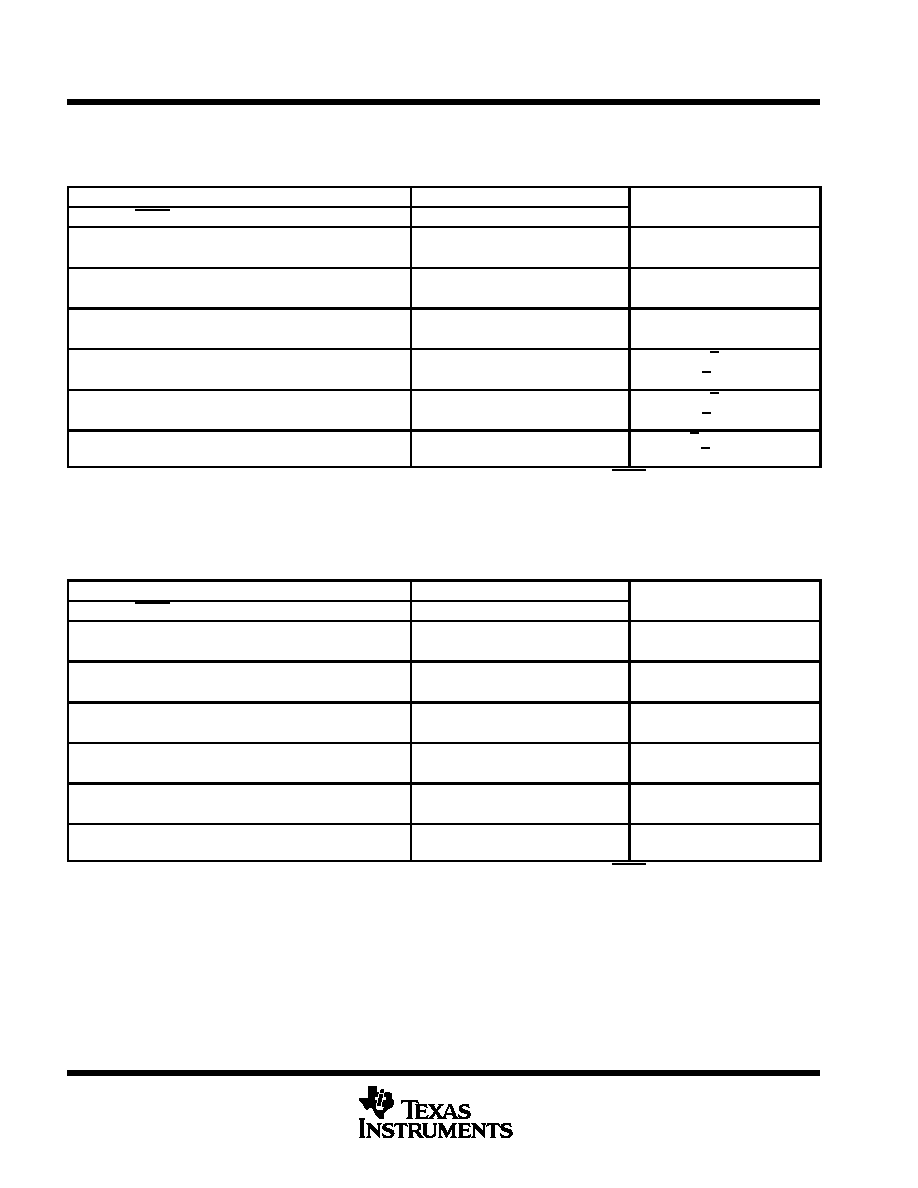
FUNCTION TABLES
SN54ALS653, SN54AS651,
SN74ALS651A, SN74ALS653, SN74AS651
INPUTS
DATA I/O
OPERATION OR FUNCTION
OEAB
OEBA
CLKAB
CLKBA
SAB
SBA
A1≠ A8
B1≠ B8
OPERATION OR FUNCTION
L
H
H or L
H or L
X
X
Input
Input
Isolation
L
H
X
X
Input
Input
Store A and B data
X
H
H or L
X
X
Input
Unspecified
Store A, hold B
H
H
X
X
Input
Output
Store A in both registers
L
X
H or L
X
X
Unspecified
Input
Hold A, store B
L
L
X
X
Output
Input
Store B in both registers
L
L
X
X
X
L
Output
Input
Real-time B data to A bus
L
L
X
H or L
X
H
Output
Input
Stored B data to A bus
H
H
X
X
L
X
Input
Output
Real-time A data to B bus
H
H
H or L
X
H
X
Input
Output
Stored A data to B bus
H
L
H or L
H or L
H
H
Output
Output
Stored A data to B bus and
stored B data to A bus
The data output functions may be enabled or disabled by a variety of level combinations at OEAB or OEBA. Data input functions are always
enabled; i.e., data at the bus terminals is stored on every low-to-high transition on the clock inputs.
Select control = L; clocks can occur simultaneously.
Select control = H; clocks must be staggered to load both registers.
SN54ALS652, SN54AS652,
SN74ALS652A, SN74ALS654, SN74AS652
INPUTS
DATA I/O
OPERATION OR FUNCTION
OEAB
OEBA
CLKAB
CLKBA
SAB
SBA
A1≠ A8
B1≠ B8
OPERATION OR FUNCTION
L
H
H or L
H or L
X
X
Input
Input
Isolation
L
H
X
X
Input
Input
Store A and B data
X
H
H or L
X
X
Input
Unspecified
Store A, hold B
H
H
X
X
Input
Output
Store A in both registers
L
X
H or L
X
X
Unspecified
Input
Hold A, store B
L
L
X
X
Output
Input
Store B in both registers
L
L
X
X
X
L
Output
Input
Real-time B data to A bus
L
L
X
H or L
X
H
Output
Input
Stored B data to A bus
H
H
X
X
L
X
Input
Output
Real-time A data to B bus
H
H
H or L
X
H
X
Input
Output
Stored A data to B bus
H
L
H or L
H or L
H
H
Output
Output
Stored A data to B bus and
stored B data to A bus
The data output functions may be enabled or disabled by a variety of level combinations at OEAB or OEBA. Data input functions are always
enabled; i.e., data at the bus terminals is stored on every low-to-high transition on the clock inputs.
Select control = L; clocks can occur simultaneously.
Select control = H; clocks must be staggered to load both registers.
SN54ALS652, SN54ALS653, SN54AS651, SN54AS652
SN74ALS651A, SN74ALS652A, SN74ALS653, SN74ALS654, SN74AS651, SN74AS652
OCTAL BUS TRANSCEIVERS AND REGISTERS WITH 3-STATE OUTPUTS
SDAS066F ≠ DECEMBER 1983 ≠ REVISED OCTOBER 1996
5
POST OFFICE BOX 655303
∑
DALLAS, TEXAS 75265
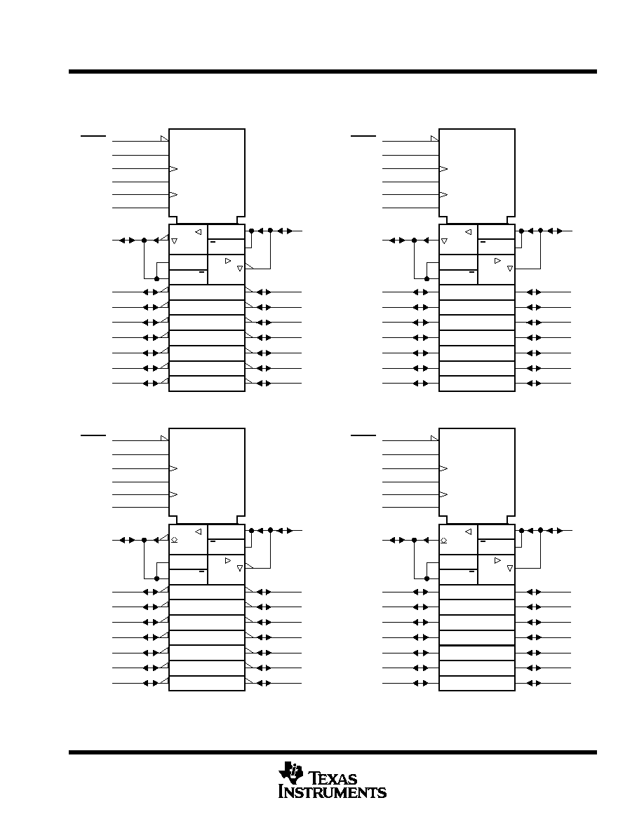
logic symbols
OEBA
EN1 [BA]
21
G5
22
SBA
A1
4
B1
20
4D
EN2 [AB]
3
OEAB
23
CLKBA
1
CLKAB
G7
2
SAB
5
7
7
5
1
1
6D
1
1
1
2
C6
C4
A2
5
B2
19
A3
6
B3
18
A4
7
B4
17
A5
8
B5
16
A6
9
B6
15
A7
10
B7
14
A8
11
B8
13
OEBA
EN1 [BA]
21
G5
22
SBA
A1
4
B1
20
4D
EN2 [AB]
3
OEAB
23
CLKBA
1
CLKAB
G7
2
SAB
5
7
7
5
1
1
6D
1
1
1
2
C6
C4
A2
5
B2
19
A3
6
B3
18
A4
7
B4
17
A5
8
B5
16
A6
9
B6
15
A7
10
B7
14
A8
11
B8
13
OEBA
EN1 [BA]
21
G5
22
SBA
A1
4
B1
20
4D
EN2 [AB]
3
OEAB
23
CLKBA
1
CLKAB
G7
2
SAB
5
7
7
5
1
1
6D
1
1
1
2
C6
C4
A2
5
B2
19
A3
6
B3
18
A4
7
B4
17
A5
8
B5
16
A6
9
B6
15
A7
10
B7
14
A8
11
B8
13
OEBA
EN1 [BA]
21
G5
22
SBA
A1
4
B1
20
4D
EN2 [AB]
3
OEAB
23
CLKBA
1
CLKAB
G7
2
SAB
5
7
7
5
1
1
6D
1
1
1
2
C6
C4
A2
5
B2
19
A3
6
B3
18
A4
7
B4
17
A5
8
B5
16
A6
9
B6
15
A7
10
B7
14
A8
11
B8
13
SN54ALS653, SN74ALS653
SN74ALS654
SN54AS651,
SN74ALS651A, SN74AS651
SN54ALS652, SN54AS652,
SN74ALS652A, SN74AS652
These symbols are in accordance with ANSI/IEEE Std 91-1984 and IEC Publication 617-12.
Pin numbers shown are for the DW, JT, and NT packages.