SN74ALS666, SN74ALS667
8-BIT D-TYPE TRANSPARENT READ-BACK LATCHES
WITH 3-STATE OUTPUTS
SDAS227A ≠ JUNE 1984 ≠ REVISED JANUARY 1995
Copyright
©
1995, Texas Instruments Incorporated
1
POST OFFICE BOX 655303
∑
DALLAS, TEXAS 75265
∑
3-State I/O-Type Read-Back Inputs
∑
Bus-Structured Pinout
∑
Choice of True or Inverting Logic
≠ SN74ALS666 . . . True Outputs
≠ SN74ALS667 . . . Inverted Outputs
∑
Preset and Clear Inputs
∑
Package Options Include Plastic
Small-Outline (DW) Packages and Standard
Plastic (NT) 300-mil DIPs
description
These 8-bit D-type transparent latches are
designed specifically for storing the contents of
the input data bus, plus reading back the stored
data onto the input data bus. In addition, they
provide a 3-state buffer-type output and are easily
utilized in bus-structured applications.
While the latch enable (LE) is high, the Q outputs
of the SN74ALS666 follow the data (D) inputs. The
Q outputs of the SN74ALS667 provide the inverse
of the data applied to its D inputs. The Q or
Q output of both devices is in the high-impedance
state if either output-enable (OE1 or OE2) input is
at a high logic level.
Read back is provided through the read-back
control (OERB) input. When OERB is taken low,
the data present at the output of the data latches
passes back onto the input data bus. When OERB
is taken high, the output of the data latches is
isolated from the D inputs. OERB does not affect
the internal operation of the latches; however,
caution should be exercised to avoid a bus
conflict.
The SN74ALS666 and SN74ALS667 are
characterized for operation from 0
∞
C to 70
∞
C.
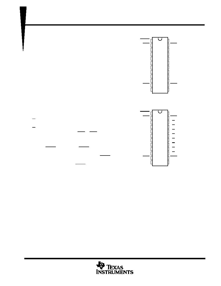
SN74ALS666 . . . DW OR NT PACKAGE
(TOP VIEW)
1
2
3
4
5
6
7
8
9
10
11
12
24
23
22
21
20
19
18
17
16
15
14
13
OERB
OE1
1D
2D
3D
4D
5D
6D
7D
8D
CLR
GND
V
CC
OE2
1Q
2Q
3Q
4Q
5Q
6Q
7Q
8Q
PRE
LE
SN74ALS667 . . . DW OR NT PACKAGE
(TOP VIEW)
1
2
3
4
5
6
7
8
9
10
11
12
24
23
22
21
20
19
18
17
16
15
14
13
OERB
OE1
1D
2D
3D
4D
5D
6D
7D
8D
CLR
GND
V
CC
OE2
1Q
2Q
3Q
4Q
5Q
6Q
7Q
8Q
PRE
LE
PRODUCTION DATA information is current as of publication date.
Products conform to specifications per the terms of Texas Instruments
standard warranty. Production processing does not necessarily include
testing of all parameters.
SN74ALS666, SN74ALS667
8-BIT D-TYPE TRANSPARENT READ-BACK LATCHES
WITH 3-STATE OUTPUTS
SDAS227A ≠ JUNE 1984 ≠ REVISED JANUARY 1995
2
POST OFFICE BOX 655303
∑
DALLAS, TEXAS 75265
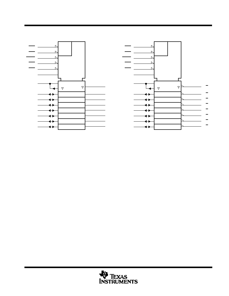
logic symbols
1Q
2Q
3Q
4Q
5Q
6Q
7Q
8Q
R
11
C1
13
LE
2D
4
3D
5
4D
6
5D
7
6D
8
7D
9
8D
10
3
18
17
16
15
21
20
19
22
1D
3
1D
S
14
EN3
1
23
2
2
&
EN2
OE1
OE2
OERB
PRE
CLR
SN74ALS667
R
11
C1
13
LE
2D
4
3D
5
4D
6
5D
7
6D
8
7D
9
8D
10
3
5Q
18
6Q
17
7Q
16
8Q
15
2Q
21
3Q
20
4Q
19
1Q
22
1D
3
1D
S
14
EN3
1
23
2
2
&
EN2
OE1
OE2
OERB
PRE
CLR
SN74ALS666
These symbols are in accordance with ANSI/IEEE Std 91-1984 and IEC Publication 617-12.
SN74ALS666, SN74ALS667
8-BIT D-TYPE TRANSPARENT READ-BACK LATCHES
WITH 3-STATE OUTPUTS
SDAS227A ≠ JUNE 1984 ≠ REVISED JANUARY 1995
3
POST OFFICE BOX 655303
∑
DALLAS, TEXAS 75265
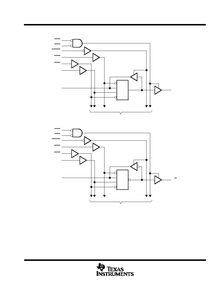
logic diagrams (positive logic)
S
1D
C1
R
To Seven Other Channels
2
23
1
14
11
13
3
22
OE1
OE2
OERB
PRE
CLR
LE
1D
1Q
SN74ALS666
S
1D
C1
R
To Seven Other Channels
2
23
1
14
11
13
3
22
OE1
OE2
OERB
PRE
CLR
LE
1D
1Q
SN74ALS667
SN74ALS666, SN74ALS667
8-BIT D-TYPE TRANSPARENT READ-BACK LATCHES
WITH 3-STATE OUTPUTS
SDAS227A ≠ JUNE 1984 ≠ REVISED JANUARY 1995
4
POST OFFICE BOX 655303
∑
DALLAS, TEXAS 75265
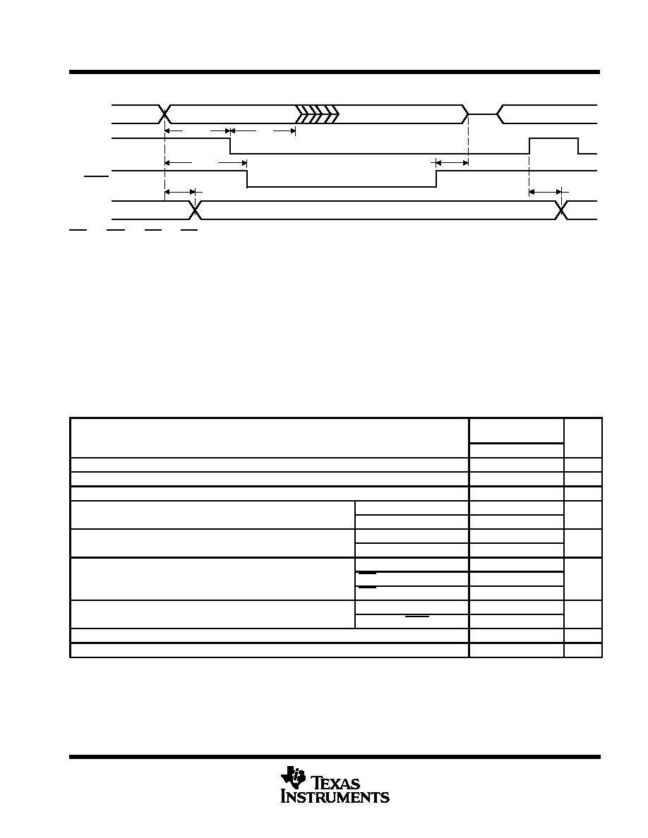
timing diagram
Input Data
tdis
th
tsu
Read Back
Data Bus
LE
Q
OERB
Input Data
tpd
tsu
tpd
CLR = H, PRE = H, OE1 = L, OE2 = L.
This setup time ensures the read-back circuit does not create a conflict on the input data bus.
absolute maximum ratings over operating free-air temperature range (unless otherwise noted)
Supply voltage, V
CC
7 V
. . . . . . . . . . . . . . . . . . . . . . . . . . . . . . . . . . . . . . . . . . . . . . . . . . . . . . . . . . . . . . . . . . . . . . . .
Input voltage, V
I
(all inputs except D inputs)
7 V
. . . . . . . . . . . . . . . . . . . . . . . . . . . . . . . . . . . . . . . . . . . . . . . . . . . .
Voltage applied to D inputs and to disabled 3-state outputs
5.5 V
. . . . . . . . . . . . . . . . . . . . . . . . . . . . . . . . . . . . .
Operating free-air temperature range, T
A
: SN74ALS666, SN74ALS667
0
∞
C to 70
∞
C
. . . . . . . . . . . . . . . . . . . .
Storage temperature range
≠ 65
∞
C to 150
∞
C
. . . . . . . . . . . . . . . . . . . . . . . . . . . . . . . . . . . . . . . . . . . . . . . . . . . . . . .
Stresses beyond those listed under "absolute maximum ratings" may cause permanent damage to the device. These are stress ratings only, and
functional operation of the device at these or any other conditions beyond those indicated under "recommended operating conditions" is not
implied. Exposure to absolute-maximum-rated conditions for extended periods may affect device reliability.
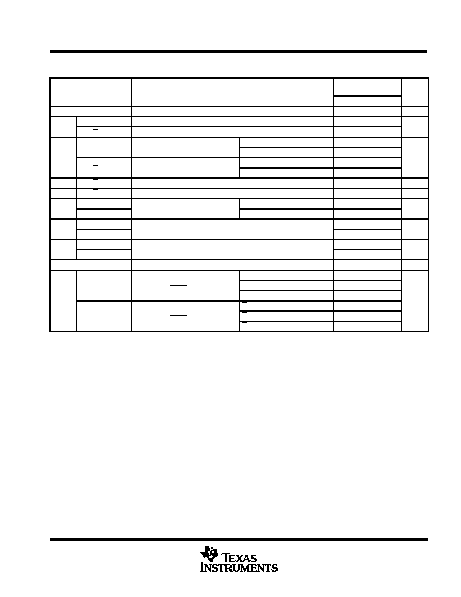
recommended operating conditions
SN74ALS666
SN74ALS667
UNIT
MIN
NOM
MAX
VCC
Supply voltage
4.5
5
5.5
V
VIH
High-level input voltage
2
V
VIL
Low-level input voltage
0.8
V
IOH
High level output current
Q
≠ 2.6
mA
IOH
High-level output current
D
≠ 0.4
mA
IOL
Low level output current
Q
24
mA
IOL
Low-level output current
D
8
mA
LE high
10
tw
Pulse duration
CLR low
10
ns
PRE low
10
t
Setup time
Data before LE
10
ns
tsu
Setup time
Data before OERB
10
ns
th
Hold time, data after LE
5
ns
TA
Operating free-air temperature
0
70
∞
C
SN74ALS666, SN74ALS667
8-BIT D-TYPE TRANSPARENT READ-BACK LATCHES
WITH 3-STATE OUTPUTS
SDAS227A ≠ JUNE 1984 ≠ REVISED JANUARY 1995
5
POST OFFICE BOX 655303
∑
DALLAS, TEXAS 75265
electrical characteristics over recommended operating free-air temperature range (unless
otherwise noted)
PARAMETER
TEST CONDITIONS
SN74ALS666
SN74ALS667
UNIT
MIN
TYP
MAX
VIK
VCC = 4.5 V,
II = ≠ 18 mA
≠ 1.2
V
V
All outputs
VCC = 4.5 V to 5.5 V,
IOH = ≠ 0.4 mA
VCC ≠ 2
V
VOH
Q or Q
VCC = 4.5 V,
IOH = ≠ 2.6 mA
2.4
3.2
V
D inputs
VCC = 4 5 V
IOL = 4 mA
0.25
0.4
VOL
D inputs
VCC = 4.5 V
IOL = 8 mA
0.35
0.5
V
VOL
Q or Q
VCC = 4 5 V
IOL = 12 mA
0.25
0.4
V
Q or Q
VCC = 4.5 V
IOL = 24 mA
0.35
0.5
IOZH
Q or Q
VCC = 5.5 V,
VO = 2.7 V
20
µ
A
IOZL
Q or Q
VCC = 5.5 V,
VO = 0.4 V
≠ 20
µ
A
II
D inputs
VCC = 5 5 V
VI = 5.5 V
0.1
mA
II
All others
VCC = 5.5 V
VI = 7 V
0.1
mA
IIH
D inputs
VCC = 5 5 V
VI = 2 7 V
20
µ
A
IIH
All others
VCC = 5.5 V,
VI = 2.7 V
20
µ
A
I
D inputs
VCC = 5 5 V
VI = 0 4 V
≠ 0.1
mA
IIL
All others
VCC = 5.5 V,
VI = 0.4 V
≠ 0.1
mA
IOß
VCC = 5.5 V,
VO = 2.25 V
≠ 30
≠112
mA
V
5 5 V
Q outputs high
25
50
SN74ALS666
VCC = 5.5 V,
OERB high
Q outputs low
40
73
ICC
OERB high
Q outputs disabled
30
55
mA
ICC
V
5 5 V
Q outputs high
25
50
mA
SN74ALS667
VCC = 5.5 V,
OERB high
Q outputs low
45
79
OERB high
Q outputs disabled
30
60
All typical values are at VCC = 5 V, TA = 25
∞
C.
For I/O ports (QA through QH), the parameters IIH and IIL include the off-state output current.
ß The output conditions have been chosen to produce a current that closely approximates one half of the true short-circuit output current, IOS.