
DGG OR DL PACKAGE
(TOP VIEW)
1
2
3
4
5
6
7
8
9
10
11
12
13
14
15
16
17
18
19
20
21
22
23
24
25
26
27
28
56
55
54
53
52
51
50
49
48
47
46
45
44
43
42
41
40
39
38
37
36
35
34
33
32
31
30
29
OEA
LE1B
2B3
GND
2B2
2B1
V
CC
A1
A2
A3
GND
A4
A5
A6
A7
A8
A9
GND
A10
A11
A12
V
CC
1B1
1B2
GND
1B3
LE2B
SEL
OE2B
LEA2B
2B4
GND
2B5
2B6
V
CC
2B7
2B8
2B9
GND
2B10
2B11
2B12
1B12
1B11
1B10
GND
1B9
1B8
1B7
V
CC
1B6
1B5
GND
1B4
LEA1B
OE1B
SN74ALVC16260
12-BIT TO 24-BIT MULTIPLEXED D-TYPE LATCH
WITH 3-STATE OUTPUTS
SCAS252A ≠ OCTOBER 1993 ≠ REVISED JULY 1995
1
POST OFFICE BOX 655303
∑
DALLAS, TEXAS 75265
D
EPIC
TM
(Enhanced-Performance Implanted
CMOS) Submicron Process
D
Member of the Texas Instruments
Widebus
TM
Family
D
ESD Protection Exceeds 2000 V Per
MIL-STD-883C, Method 3015; Exceeds
200 V Using Machine Model
(C = 200 pF, R = 0)
D
Latch-Up Performance Exceeds 250 mA
Per JEDEC Standard JESD-17
D
Flow-Through Architecture Optimizes
PCB Layout
D
Bus Hold on Data Inputs Eliminates
the Need for External Pullup/Pulldown
Resistors
D
Package Options Include Plastic Shrink
Small-Outline (DL) and Thin Shrink
Small-Outline (DGG) Packages
description
The SN74ALVC16260 is a 12-bit to 24-bit
multiplexed D-type latch used in applications
where two separate data paths must be
multiplexed onto, or demultiplexed from, a single
data path. Typical applications include
multiplexing and/or demultiplexing address and
data information in microprocessor or bus-
interface applications. This device is also useful in
memory-interleaving applications.
Three 12-bit I/O ports (A1≠A12, 1B1≠1B12, and
2B1≠2B12) are available for address and/or data
transfer. The output-enable (OE1B, OE2B, and
OEA) inputs control the bus transceiver functions.
The OE1B and OE2B control signals also allow
bank control in the A-to-B direction.
Address and/or data information can be stored using the internal storage latches. The latch-enable (LE1B,
LE2B, LEA1B, and LEA2B) inputs are used to control data storage. When the latch-enable input is high, the
latch is transparent. When the latch-enable input goes low, the data present at the inputs is latched and remains
latched until the latch-enable input is returned high.
Active bus-hold circuitry is provided to hold unused or floating data inputs at a valid logic level.
The SN74ALVC16260 is available in TI's shrink small-outline (DL) and thin shrink small-outline (DGG)
packages, which provide twice the I/O pin count and functionality of standard small-outline packages in the
same printed-circuit-board area.
The SN74ALVC16260 is characterized for operation from ≠ 40
į
C to 85
į
C.
EPIC and Widebus are trademarks of Texas Instruments Incorporated.
PRODUCTION DATA information is current as of publication date.
Products conform to specifications per the terms of Texas Instruments
standard warranty. Production processing does not necessarily include
testing of all parameters.
Copyright
©
1995, Texas Instruments Incorporated
Please be aware that an important notice concerning availability, standard warranty, and use in critical applications of
Texas Instruments semiconductor products and disclaimers thereto appears at the end of this data sheet.

SN74ALVC16260
12-BIT TO 24-BIT MULTIPLEXED D-TYPE LATCH
WITH 3-STATE OUTPUTS
SCAS252A ≠ OCTOBER 1993 ≠ REVISED JULY 1995
2
POST OFFICE BOX 655303
∑
DALLAS, TEXAS 75265
Function Tables
B TO A (OEB = H)
INPUTS
OUTPUT
1B
2B
SEL
LE1B
LE2B
OEA
A
H
X
H
H
X
L
H
L
X
H
H
X
L
L
X
X
H
L
X
L
A0
X
H
L
X
H
L
H
X
L
L
X
H
L
L
X
X
L
X
L
L
A0
X
X
X
X
X
H
Z
A TO B (OEA = H)
INPUTS
OUTPUTS
A
LEA1B
LEA2B
OE1B
OE2B
1B
2B
H
H
H
L
L
H
H
L
H
H
L
L
L
L
H
H
L
L
L
H
2B0
L
H
L
L
L
L
2B0
H
L
H
L
L
1B0
H
L
L
H
L
L
1B0
L
X
L
L
L
L
1B0
2B0
X
X
X
H
H
Z
Z
X
X
X
L
H
Active
Z
X
X
X
H
L
Z
Active
X
X
X
L
L
Active
Active
SN74ALVC16260
12-BIT TO 24-BIT MULTIPLEXED D-TYPE LATCH
WITH 3-STATE OUTPUTS
SCAS252A ≠ OCTOBER 1993 ≠ REVISED JULY 1995
3
POST OFFICE BOX 655303
∑
DALLAS, TEXAS 75265
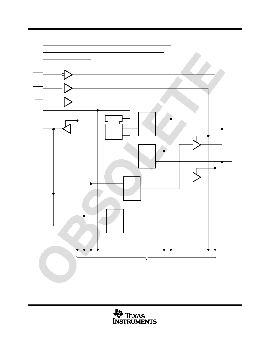
logic diagram (positive logic)
C1
1D
C1
1D
C1
1D
C1
1D
G1
To 11 Other Channels
LE1B
LE2B
LEA1B
LEA2B
OE2B
OE1B
OEA
SEL
A1
1B1
2B1
1
1
27
2
30
55
56
1
28
8
23
6
29

SN74ALVC16260
12-BIT TO 24-BIT MULTIPLEXED D-TYPE LATCH
WITH 3-STATE OUTPUTS
SCAS252A ≠ OCTOBER 1993 ≠ REVISED JULY 1995
4
POST OFFICE BOX 655303
∑
DALLAS, TEXAS 75265
absolute maximum ratings over operating free-air temperature range (unless otherwise noted)
Supply voltage range, V
CC
≠ 0.5 V to 4.6 V
. . . . . . . . . . . . . . . . . . . . . . . . . . . . . . . . . . . . . . . . . . . . . . . . . . . . . . . .
Input voltage range, V
I
: (except I/O ports) (see Note 1)
≠ 0.5 V to 4.6 V
. . . . . . . . . . . . . . . . . . . . . . . . . . . . . . .
(I/O ports) (see Notes 1 and 2)
≠ 0.5 V to V
CC
+ 0.5 V
. . . . . . . . . . . . . . . . . . . . . . . . .
Output voltage range, V
O
(see Notes 1 and 2)
≠ 0.5 V to V
CC
+ 0.5 V
. . . . . . . . . . . . . . . . . . . . . . . . . . . . . . . . .
Output clamp current, I
OK
(V
O
< 0 or V
O
> V
CC
)
Ī
50 mA
. . . . . . . . . . . . . . . . . . . . . . . . . . . . . . . . . . . . . . . . . . .
Continuous output current, I
O
(V
O
= 0 to V
CC
)
Ī
50 mA
. . . . . . . . . . . . . . . . . . . . . . . . . . . . . . . . . . . . . . . . . . . . .
Continuous current through V
CC
or GND
Ī
100 mA
. . . . . . . . . . . . . . . . . . . . . . . . . . . . . . . . . . . . . . . . . . . . . . . . .
Maximum power dissipation at T
A
= 55
į
C (in still air) (see Note 3): DGG package
1 W
. . . . . . . . . . . . . . . . . .
DL package
1.4 W
. . . . . . . . . . . . . . . . . .
Storage temperature range, T
stg
≠ 65
į
C to 150
į
C
. . . . . . . . . . . . . . . . . . . . . . . . . . . . . . . . . . . . . . . . . . . . . . . . . .
Stresses beyond those listed under "absolute maximum ratings" may cause permanent damage to the device. These are stress ratings only, and
functional operation of the device at these or any other conditions beyond those indicated under "recommended operating conditions" is not
implied. Exposure to absolute-maximum-rated conditions for extended periods may affect device reliability.
NOTES:
1. The input and output negative-voltage ratings may be exceeded if the input and output clamp-current ratings are observed.
2. The input and output positive voltage ratings may be exceeded up to 4.6 V if the input and output clamp-current ratings are observed.
3. The maximum package power dissipation is calculated using a junction temperature of 150
į
C and a board trace length of 750 mils.
For more information, refer to the
Package Thermal Considerations application note in the 1994 ABT Advanced BiCMOS Technology
Data Book, literature number SCBD002B.
recommended operating conditions (see Note 4)
MIN
MAX
UNIT
VCC
Supply voltage
2.3
3.6
V
VIH
High level input voltage
VCC = 2.3 V to 2.7 V
1.7
V
VIH
High-level input voltage
VCC = 2.7 V to 3.6 V
2
V
VIL
Low level input voltage
VCC = 2.3 V to 2.7 V
0.7
V
VIL
Low-level input voltage
VCC = 2.7 V to 3.6 V
0.8
V
VI
Input voltage
0
VCC
V
VO
Output voltage
0
VCC
V
VCC = 2.3 V
≠ 12
IOH
High-level output current
VCC = 2.7 V
≠ 12
mA
VCC = 3 V
≠ 24
VCC = 2.3 V
12
IOL
Low-level output current
VCC = 2.7 V
12
mA
VCC = 3 V
24
t /
v
Input transition rise or fall rate
0
10
ns / V
TA
Operating free-air temperature
≠ 40
85
į
C
NOTE 4: Unused control inputs must be held high or low to prevent them from floating.

SN74ALVC16260
12-BIT TO 24-BIT MULTIPLEXED D-TYPE LATCH
WITH 3-STATE OUTPUTS
SCAS252A ≠ OCTOBER 1993 ≠ REVISED JULY 1995
5
POST OFFICE BOX 655303
∑
DALLAS, TEXAS 75265
electrical characteristics over recommended operating free-air temperature range (unless
otherwise noted)
PARAMETER
TEST CONDITIONS
VCC
MIN
TYP
MAX
UNIT
IOH = ≠ 100
Ķ
A
MIN to MAX
VCC ≠ 0.2
IOH = ≠ 6 mA,
VIH = 1.7 V
2.3 V
2
VOH
VIH = 1.7 V
2.3 V
1.7
V
VOH
IOH = ≠ 12 mA
VIH = 2 V
2.7 V
2.2
V
VIH = 2 V
3 V
2.4
IOH = ≠ 24 mA,
VIH = 2 V
3 V
2
IOL = 100
Ķ
A
MIN to MAX
0.2
IOL = 6 mA,
VIL = 0.7 V
2.3 V
0.4
VOL
IOL = 12 mA
VIL = 0.7 V
2.3 V
0.7
V
IOL = 12 mA
VIL = 0.8 V
2.7 V
0.4
IOL = 24 mA,
VIL = 0.8 V
3 V
0.55
II
VI = VCC or GND
3.6 V
Ī
5
Ķ
A
VI = 0.7 V
2 3 V
45
VI = 1.7 V
2.3 V
≠ 45
II(hold)
VI = 0.8 V
3 V
75
Ķ
A
(
)
VI = 2 V
3 V
≠ 75
VI = 0 to 3.6 V
3.6 V
Ī
500
IOZß
VO = VCC or GND
3.6 V
Ī
10
Ķ
A
ICC
VI = VCC or GND,
IO = 0
3.6 V
40
Ķ
A
n
ICC
One input at VCC ≠ 0.6 V,
Other inputs at VCC or GND
3 V to 3.6 V
750
Ķ
A
Ci
Control inputs
VI = VCC or GND
3.3 V
3.5
pF
Cio
A or B ports
VO = VCC or GND
3.3 V
9
pF
For conditions shown as MIN or MAX, use the appropriate values under recommended operating conditions.
All typical values are at VCC = 3.3 V.
ß For I/O ports, the parameter IOZ includes the input-leakage current.
timing requirements over recommended ranges of supply voltage and operating free-air
temperature (unless otherwise noted)
VCC = 2.5 V
Ī
0.2 V
VCC = 2.7 V
VCC = 3.3 V
Ī
0.3 V
UNIT
MIN
MAX
MIN
MAX
MIN
MAX
fclock
Clock frequency
0
150
0
150
0
150
MHz
tw
Pulse duration, LE1B, LE2B, LEA1B, or LEA2B high
3.3
3.3
3.3
ns
tsu
Setup time, data before LE1B, LE2B, LEA1B, or LEA2B low
1.4
1.1
1.1
ns
th
Hold time, data after LE1B, LE2B, LEA1B, or LEA2B low
1.6
1.9
1.5
ns