SN74BCT533
OCTAL TRANSPARENT D-TYPE LATCH
WITH 3-STATE OUTPUTS
SCBS055A ≠ JULY 1990 ≠ REVISED NOVEMBER 1993
Copyright
©
1993, Texas Instruments Incorporated
1
POST OFFICE BOX 655303
∑
DALLAS, TEXAS 75265
∑
State-of-the-Art BiCMOS Design
Significantly Reduces I
CCZ
∑
Full Parallel Access for Loading
∑
3-State Inverting Outputs Drive Bus Lines
or Buffer Memory Address Registers
∑
ESD Protection Exceeds 2000 V
Per MIL-Std-883C, Method 3015
∑
Package Options Include Plastic
Small-Outline (DW) Packages and Standard
Plastic 300-mil DIPs (N)
description
The SN74BCT533 is an 8-bit transparent D-type
latch with 3-state outputs designed specifically for
driving highly capacitive or relatively low-imped-
ance loads. It is particularly suitable for
implementing buffer registers, I/O ports, bidirec-
tional bus drivers, and working registers.
When the latch-enable (LE) input is high, the Q outputs follow the complements of the data (D) inputs. When
LE is taken low, the Q outputs are latched at the inverse of the levels set up at the D inputs. The SN74BCT533
provides inverted data at its outputs.
A buffered output-enable (OE) input can be used to place the eight outputs in either a normal logic state (high
or low logic levels) or a high-impedance state. In the high-impedance state, the outputs neither load nor drive
the bus lines significantly. The high-impedance state and the increased drive provide the capability to drive bus
lines without need for interface or pullup components.
The output-enable (OE) input does not affect the internal operations of the latch. Previously stored data can be
retained or new data can be entered while the outputs are in the high-impedance state.
The SN74BCT533 is characterized for operation from 0
∞
C to 70
∞
C.
FUNCTION TABLE
(each latch)
INPUTS
OUTPUT
OE
LE
D
Q
L
H
H
L
L
H
L
H
L
L
X
Q0
H
X
X
Z
1
2
3
4
5
6
7
8
9
10
20
19
18
17
16
15
14
13
12
11
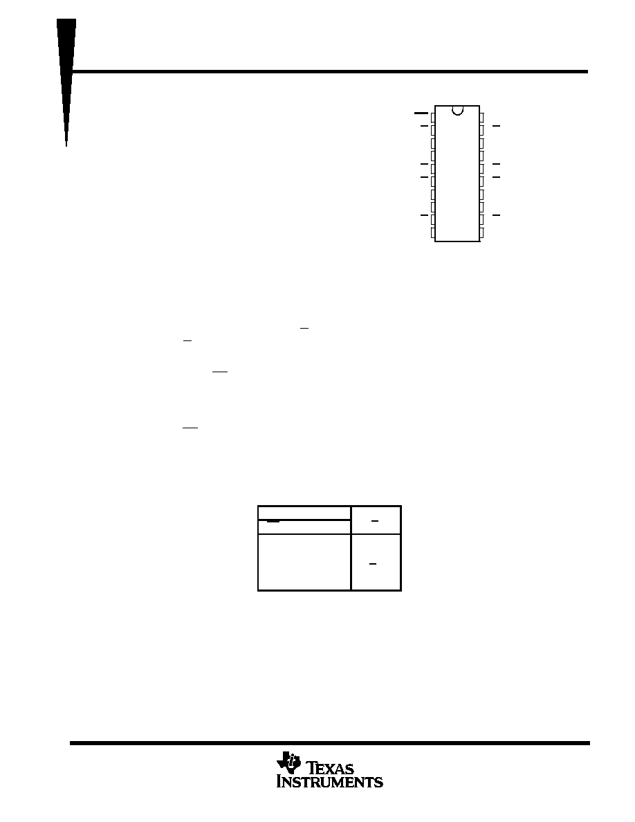
OE
1Q
1D
2D
2Q
3Q
3D
4D
4Q
GND
V
CC
8Q
8D
7D
7Q
6Q
6D
5D
5Q
LE
DW OR N PACKAGE
(TOP VIEW)
PRODUCTION DATA information is current as of publication date.
Products conform to specifications per the terms of Texas Instruments
standard warranty. Production processing does not necessarily include
testing of all parameters.
SN74BCT533
OCTAL TRANSPARENT D-TYPE LATCH
WITH 3-STATE OUTPUTS
SCBS055A ≠ JULY 1990 ≠ REVISED NOVEMBER 1993
2
POST OFFICE BOX 655303
∑
DALLAS, TEXAS 75265
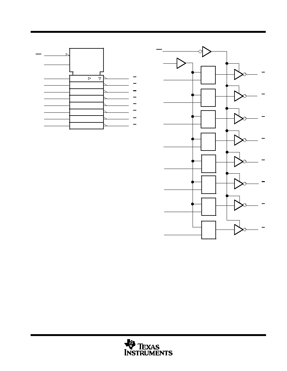
logic symbol
logic diagram (positive logic)
1D
3
1D
4
2D
7
3D
8
4D
13
5D
14
6D
17
7D
18
8D
2
5
6
9
12
15
16
19
EN
1
C1
11
LE
OE
1Q
2Q
3Q
4Q
5Q
6Q
8Q
7Q
This symbol is in accordance with ANSI/IEEE Std 91-1984
and IEC Publication 617-12.
1D
C1
C1
C1
C1
C1
C1
C1
C1
1D
1D
1D
1D
1D
1D
1D
OE
1D
2D
3D
4D
5D
6D
7D
8D
1Q
2Q
3Q
4Q
5Q
6Q
7Q
8Q
LE
1
1
11
3
4
7
8
13
14
17
18
2
5
6
9
12
15
16
19

SN74BCT533
OCTAL TRANSPARENT D-TYPE LATCH
WITH 3-STATE OUTPUTS
SCBS055A ≠ JULY 1990 ≠ REVISED NOVEMBER 1993
3
POST OFFICE BOX 655303
∑
DALLAS, TEXAS 75265
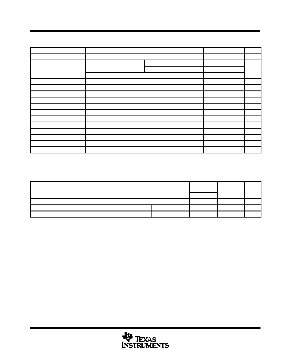
absolute maximum ratings over operating free-air temperature range (unless otherwise noted)
Supply voltage range, V
CC
≠ 0.5 V to 7 V
. . . . . . . . . . . . . . . . . . . . . . . . . . . . . . . . . . . . . . . . . . . . . . . . . . . . . . . . . .
Input voltage range, V
I
(see Note 1)
≠ 0.5 V to 7 V
. . . . . . . . . . . . . . . . . . . . . . . . . . . . . . . . . . . . . . . . . . . . . . . . . . .
Voltage range applied to any output in the disabled or power-off state, V
O
≠ 0.5 V to 7 V
. . . . . . . . . . . . . . . . .
Voltage range applied to any output in the high state, V
O
≠ 0.5 V to V
CC
. . . . . . . . . . . . . . . . . . . . . . . . . . . . . . .
Input clamp current
≠ 30 mA
. . . . . . . . . . . . . . . . . . . . . . . . . . . . . . . . . . . . . . . . . . . . . . . . . . . . . . . . . . . . . . . . . . . .
Current into any output in the low state
128 mA
. . . . . . . . . . . . . . . . . . . . . . . . . . . . . . . . . . . . . . . . . . . . . . . . . . . . .
Operating free-air temperature range
0
∞
C to 70
∞
C
. . . . . . . . . . . . . . . . . . . . . . . . . . . . . . . . . . . . . . . . . . . . . . . . . . .
Storage temperature range
≠ 65
∞
C to 150
∞
C
. . . . . . . . . . . . . . . . . . . . . . . . . . . . . . . . . . . . . . . . . . . . . . . . . . . . . . . .
Stresses beyond those listed under "absolute maximum ratings" may cause permanent damage to the device. These are stress ratings only and
functional operation of the device at these or any other conditions beyond those indicated under "recommended operating conditions" is not
implied. Exposure to absolute-maximum-rated conditions for extended periods may affect device reliability.
NOTE 1: The input and output voltage ratings may be exceeded if the input and output current ratings are observed.
recommended operating conditions
MIN
NOM
MAX
UNIT
VCC
Supply voltage
4.5
5
5.5
V
VIH
High-level input voltage
2
V
VIL
Low-level input voltage
0.8
V
IIK
Input clamp current
≠18
mA
IOH
High-level output current
≠15
mA
IOL
Low-level output current
64
mA
TA
Operating free-air temperature
0
70
∞
C
SN74BCT533
OCTAL TRANSPARENT D-TYPE LATCH
WITH 3-STATE OUTPUTS
SCBS055A ≠ JULY 1990 ≠ REVISED NOVEMBER 1993
4
POST OFFICE BOX 655303
∑
DALLAS, TEXAS 75265
electrical characteristics over recommended operating free-air temperature range (unless
otherwise noted)
PARAMETER
TEST CONDITIONS
MIN
TYP
MAX
UNIT
VIK
VCC = 4.5 V,
II = ≠18 mA
≠1.2
V
VCC = 4 5 V
IOH = ≠ 3 mA
2.4
3.3
VOH
VCC = 4.5 V
IOH = ≠15 mA
2
3.1
V
VCC = 4.75 V,
IOH = ≠ 3 mA
2.7
VOL
VCC = 4.5 V,
IOL = 64 mA
0.42
0.55
V
II
VCC = 5.5 V,
VI = 5.5 V
0.4
mA
IIH
VCC = 5.5 V,
VI = 2.7 V
20
µ
A
IIL
VCC = 5.5 V,
VI = 0.5 V
≠ 0.6
mA
IOS
VCC = 5.5 V,
VO = 0
≠100
≠ 225
mA
IOZH
VCC = 5.5 V,
VO = 2.7 V
50
µ
A
IOZL
VCC = 5.5 V,
VO = 0.5 V
≠ 50
µ
A
ICCL
VCC = 5.5 V
40
63
mA
ICCH
VCC = 5.5 V
5
8
mA
ICCZ
VCC = 5.5 V
5
8
mA
Ci
VCC = 5 V,
VI = 2.5 V or 0.5 V
6
pF
Co
VCC = 5 V,
VO = 2.5 V or 0.5 V
11
pF
All typical values are at VCC = 5 V, TA = 25
∞
C.
Not more than one output should be tested at a time, and the duration of the test should not exceed one second.
timing requirements over recommended ranges of supply voltage and operating free-air
temperature (unless otherwise noted)
VCC = 5 V,
TA = 25
∞
C
MIN
MAX
UNIT
MIN
MAX
tw
Pulse duration, LE high
4
4
ns
tsu
Setup time, data before LE
High or low
2.5
2.5
ns
th
Hold time, data after LE
High or low
3
3
ns

SN74BCT533
OCTAL TRANSPARENT D-TYPE LATCH
WITH 3-STATE OUTPUTS
SCBS055A ≠ JULY 1990 ≠ REVISED NOVEMBER 1993
5
POST OFFICE BOX 655303
∑
DALLAS, TEXAS 75265
switching characteristics (see Note 2)
PARAMETER
FROM
(INPUT)
TO
(OUTPUT)
VCC = 5 V,
CL = 50 pF,
R1 = 500
,
R2 = 500
,
TA = 25
∞
C
VCC = 4.5 V to 5.5 V,
CL = 50 pF,
R1 = 500
,
R2 = 500
,
TA = MIN to MAX
UNIT
MIN
TYP
MAX
MIN
MAX
tPLH
D
Q
2.8
6.1
9.1
2.8
11.2
ns
tPHL
D
Q
2.7
5.3
8.2
2.7
9.3
ns
tPLH
LE
Q
2.3
5
7.7
2.3
8.6
ns
tPHL
LE
Q
2.5
4.9
7.6
2.5
8.1
ns
tPZH
OE
Q
3.1
6.1
8.8
3.1
10.8
ns
tPZL
OE
Q
3.7
6.9
10
3.7
12
ns
tPHZ
OE
Q
1.8
3.9
5.9
1.8
6.9
ns
tPLZ
OE
Q
1.3
3.5
6.1
1.3
7.2
ns
For conditions shown as MIN or MAX, use the appropriate value specified under recommended operating conditions.
NOTE 2: Load circuits and voltage waveforms are shown in Section 1.