SN74CBTLV16800
LOW-VOLTAGE 20-BIT FET BUS SWITCH
WITH PRECHARGED OUTPUTS
SCDS045F ≠ DECEMBER 1997 ≠ REVISED MAY 1999
1
POST OFFICE BOX 655303
∑
DALLAS, TEXAS 75265
D
5-
Switch Connection Between Two Ports
D
Isolation Under Power-Off Conditions
D
B-Port Outputs Are Precharged by Bias
Voltage to Minimize Signal Distortion
During Live Insertion
D
ESD Protection Exceeds 2000 V Per
MIL-STD-883, Method 3015; Exceeds 200 V
Using Machine Model (C = 200 pF, R = 0)
D
Latch-Up Performance Exceeds 100 mA Per
JESD 78, Class II
D
Package Options Include Plastic Thin
Shrink Small-Outline (DGG), Thin Very
Small-Outline (DGV), and 300-mil Shrink
Small-Outline (DL) Packages
NOTE: For tape and reel order entry:
The DGGR package is abbreviated to GR, and
the DGVR package is abbreviated to VR.
description
The SN74CBTLV16800 provides 20 bits of
high-speed bus switching. The low on-state
resistance of the switch allows connections to be
made with minimal propagation delay. The device
also precharges the B port to a user-selectable
bias voltage (BIASV) to minimize live-insertion
noise.
The device is organized as dual 10-bit bus switches with separate output-enable (OE) inputs. It can be used
as two 10-bit bus switches or one 20-bit bus switch. When OE is low, the associated 10-bit bus switch is on,
and port A is connected to port B. When OE is high, the switch is open, the high-impedance state exists between
the two ports, and port B is precharged to BIASV through the equivalent of a 10-k
resistor.
To ensure the high-impedance state during power up or power down, OE should be tied to V
CC
through a pullup
resistor; the minimum value of the resistor is determined by the current-sinking capability of the driver.
The SN74CBTLV16800 is characterized for operation from ≠40
∞
C to 85
∞
C.
FUNCTION TABLE
(each 10-bit bus switch)
INPUT
OE
FUNCTION
L
A port = B port
H
A port = Z
B port = BIASV
Copyright
©
1999, Texas Instruments Incorporated
PRODUCTION DATA information is current as of publication date.
Products conform to specifications per the terms of Texas Instruments
standard warranty. Production processing does not necessarily include
testing of all parameters.
Please be aware that an important notice concerning availability, standard warranty, and use in critical applications of
Texas Instruments semiconductor products and disclaimers thereto appears at the end of this data sheet.
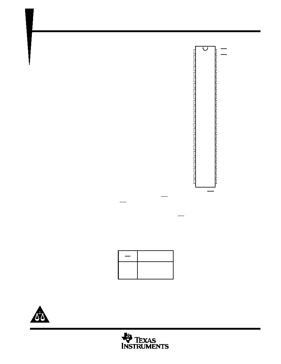
DGG, DGV, OR DL PACKAGE
(TOP VIEW)
1
2
3
4
5
6
7
8
9
10
11
12
13
14
15
16
17
18
19
20
21
22
23
24
48
47
46
45
44
43
42
41
40
39
38
37
36
35
34
33
32
31
30
29
28
27
26
25
BIASV
1A1
1A2
1A3
1A4
1A5
1A6
GND
1A7
1A8
1A9
1A10
2A1
2A2
V
CC
2A3
GND
2A4
2A5
2A6
2A7
2A8
2A9
2A10
1OE
2OE
1B1
1B2
1B3
1B4
1B5
GND
1B6
1B7
1B8
1B9
1B10
2B1
2B2
2B3
GND
2B4
2B5
2B6
2B7
2B8
2B9
2B10
SN74CBTLV16800
LOW-VOLTAGE 20-BIT FET BUS SWITCH
WITH PRECHARGED OUTPUTS
SCDS045F ≠ DECEMBER 1997 ≠ REVISED MAY 1999
2
POST OFFICE BOX 655303
∑
DALLAS, TEXAS 75265
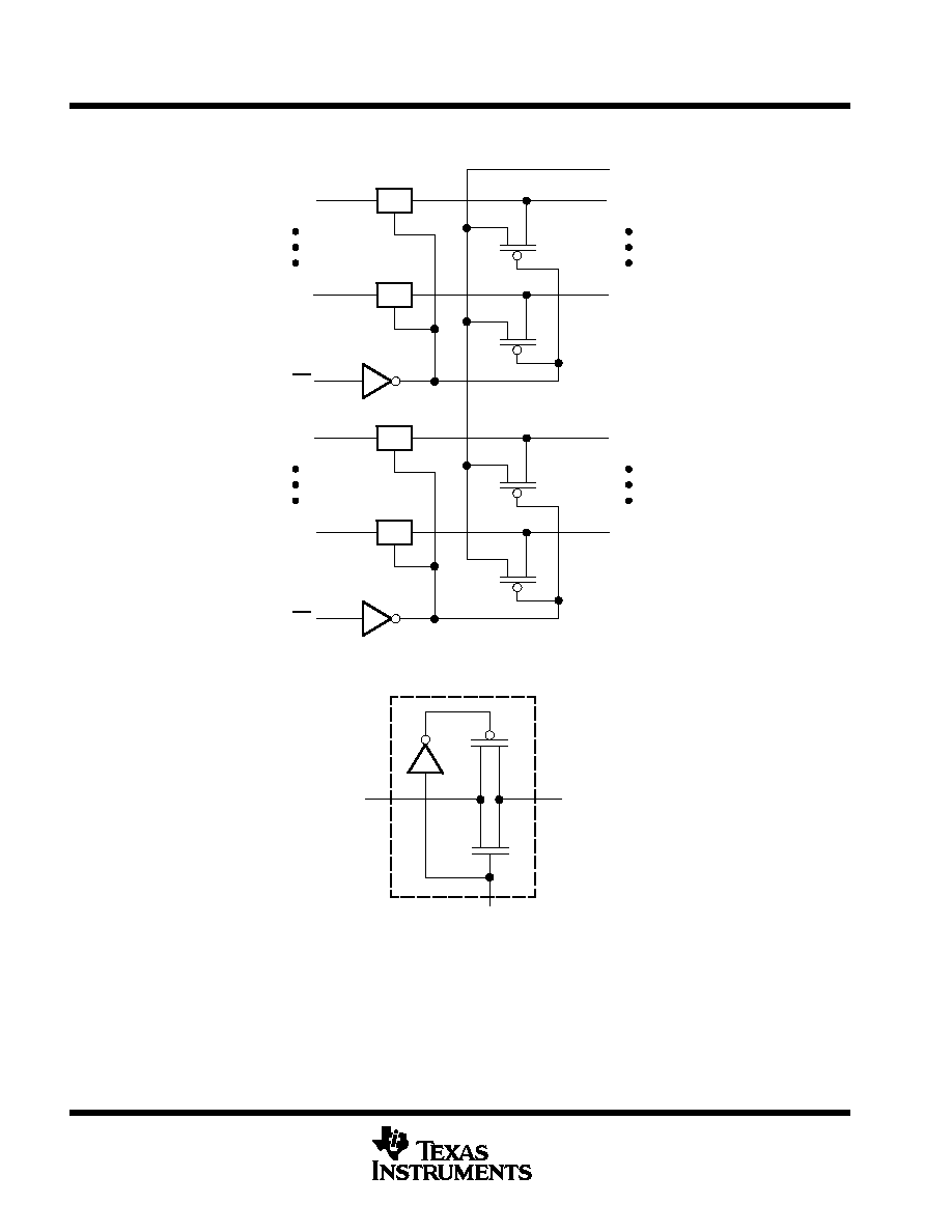
logic diagram (positive logic)
1A1
1B1
1A10
1OE
1B10
BIASV
2A1
2B1
2A10
2OE
2B10
SW
SW
SW
2
12
48
13
24
47
1
46
36
35
25
SW
simplified schematic, each FET switch
A
(OE)
B
SN74CBTLV16800
LOW-VOLTAGE 20-BIT FET BUS SWITCH
WITH PRECHARGED OUTPUTS
SCDS045F ≠ DECEMBER 1997 ≠ REVISED MAY 1999
3
POST OFFICE BOX 655303
∑
DALLAS, TEXAS 75265
absolute maximum ratings over operating free-air temperature range (unless otherwise noted)
Supply voltage range, V
CC
≠0.5 V to 4.6 V
. . . . . . . . . . . . . . . . . . . . . . . . . . . . . . . . . . . . . . . . . . . . . . . . . . . . . . . . .
Bias voltage range, BIASV
≠0.5 V to 4.6 V
. . . . . . . . . . . . . . . . . . . . . . . . . . . . . . . . . . . . . . . . . . . . . . . . . . . . . . . . .
Input voltage range, V
I
(see Note 1)
≠0.5 V to 4.6 V
. . . . . . . . . . . . . . . . . . . . . . . . . . . . . . . . . . . . . . . . . . . . . . . . .
Continuous channel current
128 mA
. . . . . . . . . . . . . . . . . . . . . . . . . . . . . . . . . . . . . . . . . . . . . . . . . . . . . . . . . . . . . .
Input clamp current, I
IK
(V
I
< 0)
≠50 mA
. . . . . . . . . . . . . . . . . . . . . . . . . . . . . . . . . . . . . . . . . . . . . . . . . . . . . . . . . . .
Package thermal impedance,
JA
(see Note 2): DGG package
89
∞
C/W
. . . . . . . . . . . . . . . . . . . . . . . . . . . . . . . .
DGV package
93
∞
C/W
. . . . . . . . . . . . . . . . . . . . . . . . . . . . . . . .
DL package
94
∞
C/W
. . . . . . . . . . . . . . . . . . . . . . . . . . . . . . . . . .
Storage temperature range, T
stg
≠65
∞
C to 150
∞
C
. . . . . . . . . . . . . . . . . . . . . . . . . . . . . . . . . . . . . . . . . . . . . . . . . . .
Stresses beyond those listed under "absolute maximum ratings" may cause permanent damage to the device. These are stress ratings only, and
functional operation of the device at these or any other conditions beyond those indicated under "recommended operating conditions" is not
implied. Exposure to absolute-maximum-rated conditions for extended periods may affect device reliability.
NOTES:
1. The input and output negative-voltage ratings may be exceeded if the input and output clamp-current ratings are observed.
2. The package thermal impedance is calculated in accordance with JESD 51.
recommended operating conditions (see Note 3)
MIN
MAX
UNIT
VCC
Supply voltage
2.3
3.6
V
BIASV
Bias voltage
1.3
VCC
V
VIH
High level control input voltage
VCC = 2.3 V to 2.7 V
1.7
V
VIH
High-level control input voltage
VCC = 2.7 V to 3.6 V
2
V
VIL
Low level control input voltage
VCC = 2.3 V to 2.7 V
0.7
V
VIL
Low-level control input voltage
VCC = 2.7 V to 3.6 V
0.8
V
TA
Operating free-air temperature
≠40
85
∞
C
NOTE 3: All unused control inputs of the device must be held at VCC or GND to ensure proper device operation. Refer to the TI application report,
Implications of Slow or Floating CMOS Inputs, literature number SCBA004.
electrical characteristics over recommended operating free-air temperature range (unless
otherwise noted)
PARAMETER
TEST CONDITIONS
MIN
TYP
MAX
UNIT
VIK
VCC = 3 V,
II = ≠18 mA
≠1.2
V
II
VCC = 3.6 V,
VI = VCC or GND
±
1
µ
A
Ioff
A port
VCC = 0,
VI or VO= 0 to 3.6 V
10
µ
A
IO
VCC = 3 V,
BIASV = 2.4 V,
VO= 0,
OE = VCC
0.25
mA
ICC
VCC = 3.6 V,
IO = 0,
VI = VCC or GND
10
µ
A
ICCß
Control inputs
VCC = 3.6 V,
One input at 3 V,
Other inputs at VCC or GND
300
µ
A
Ci
Control inputs
VI = 3 V or 0
4.5
pF
Cio(OFF)
VO = 3 V or 0,
Switch off,
BIASV = Open
6.5
pF
∂
V
2 3 V
VI = 0
II = 64 mA
5
9
∂
VCC = 2.3 V,
TYP at VCC = 2.5 V
VI = 0
II = 24 mA
5
9
r
∂
TYP at VCC = 2.5 V
VI = 1.7 V,
II = 15 mA
25
35
ron∂
VI = 0
II = 64 mA
5
7
VCC = 3 V
VI = 0
II = 24 mA
5
7
VI = 2.4 V,
II = 15 mA
8
15
All typical values are at VCC = 3.3 V (unless otherwise noted), TA = 25
∞
C.
ß This is the increase in supply current for each input that is at the specified voltage level rather than VCC or GND.
∂ Measured by the voltage drop between the A and B terminals at the indicated current through the switch. On-state resistance is determined by
the lower of the voltages of the two (A or B) terminals.
SN74CBTLV16800
LOW-VOLTAGE 20-BIT FET BUS SWITCH
WITH PRECHARGED OUTPUTS
SCDS045F ≠ DECEMBER 1997 ≠ REVISED MAY 1999
4
POST OFFICE BOX 655303
∑
DALLAS, TEXAS 75265
switching characteristics over recommended operating free-air temperature range (unless
otherwise noted) (see Figures 1 and 2)
PARAMETER
TEST
CONDITIONS
FROM
(INPUT)
TO
(OUTPUT)
VCC = 2.5 V
±
0.2 V
VCC = 3.3 V
±
0.3 V
UNIT
CONDITIONS
(INPUT)
(OUTPUT)
MIN
MAX
MIN
MAX
tpd
A or B
B or A
0.35
0.25
ns
tPZH
BIASV = GND
OE
A or B
2.9
7.7
2.2
5.5
ns
tPZL
BIASV = 3 V
OE
A or B
2.8
6.4
2.1
5.3
ns
tPHZ
BIASV = GND
OE
A or B
1.4
6.8
2.6
7.6
ns
tPLZ
BIASV = 3 V
OE
A or B
1.3
4.2
1.5
5.1
ns
The propagation delay is the calculated RC time constant of the typical on-state resistance of the switch and the specified load capacitance, when
driven by an ideal voltage source (zero output impedance).
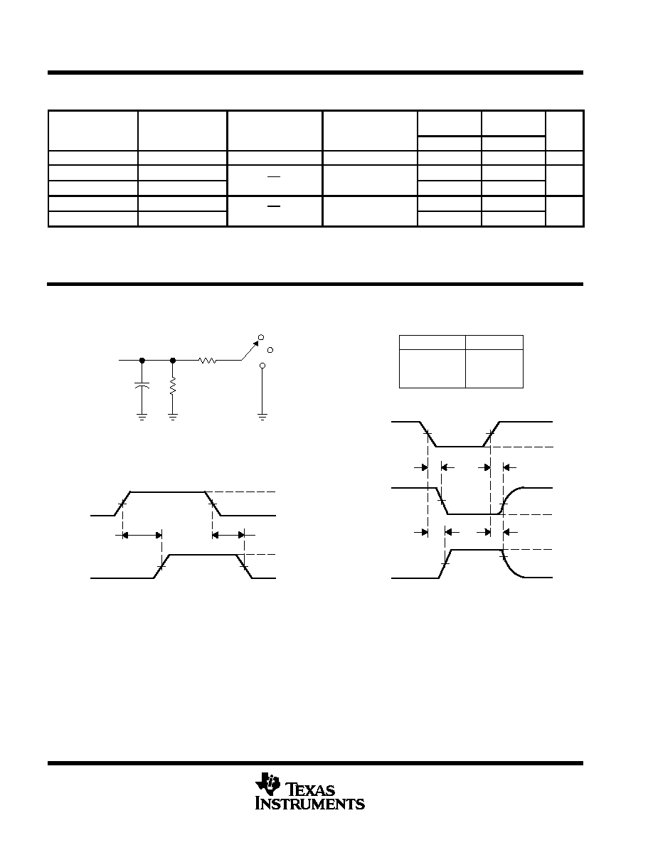
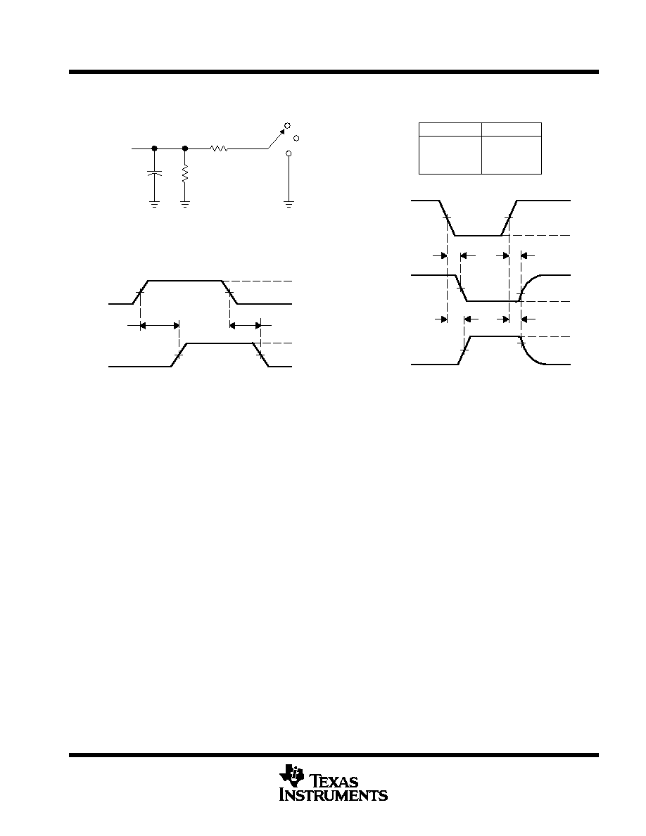
PARAMETER MEASUREMENT INFORMATION
V
CC
= 2.5 V
±
0.2 V
VCC/2
VCC/2
VCC/2
VCC/2
VOH
VOL
From Output
Under Test
CL = 30 pF
(see Note A)
LOAD CIRCUIT
S1
Open
GND
500
500
Output
Control
(low-level
enabling)
Output
Waveform 1
S1 at 2
◊
VCC
(see Note B)
Output
Waveform 2
S1 at GND
(see Note B)
tPZL
tPZH
tPLZ
tPHZ
0 V
VOL + 0.15 V
VOH ≠ 0.15 V
0 V
VCC
VOLTAGE WAVEFORMS
ENABLE AND DISABLE TIMES
tpd
tPLZ/tPZL
tPHZ/tPZH
Open
2
◊
VCC
GND
TEST
S1
NOTES: A. CL includes probe and jig capacitance.
B. Waveform 1 is for an output with internal conditions such that the output is low except when disabled by the output control.
Waveform 2 is for an output with internal conditions such that the output is high except when disabled by the output control.
C. All input pulses are supplied by generators having the following characteristics: PRR
10 MHz, ZO = 50
, tr
2 ns, tf
2 ns.
D. The outputs are measured one at a time with one transition per measurement.
E. tPLH and tPHL are the same as tpd.
tPHL
VCC/2
VCC/2
VCC
0 V
VOH
VOL
Input
Output
VOLTAGE WAVEFORMS
PROPAGATION DELAY TIMES
VCC/2
VCC/2
tPLH
2
◊
VCC
VCC
Figure 1. Load Circuit and Voltage Waveforms
SN74CBTLV16800
LOW-VOLTAGE 20-BIT FET BUS SWITCH
WITH PRECHARGED OUTPUTS
SCDS045F ≠ DECEMBER 1997 ≠ REVISED MAY 1999
5
POST OFFICE BOX 655303
∑
DALLAS, TEXAS 75265
PARAMETER MEASUREMENT INFORMATION
V
CC
= 3.3 V
±
0.3 V
VOH
VOL
From Output
Under Test
CL = 50 pF
(see Note A)
LOAD CIRCUIT
S1
6 V
Open
GND
500
500
tPLH
tPHL
Output
Control
(low-level
enabling)
Output
Waveform 1
S1 at 6 V
(see Note B)
Output
Waveform 2
S1 at GND
(see Note B)
tPZL
tPZH
tPLZ
tPHZ
3 V
0 V
VOH
VOL
0 V
VOL + 0.3 V
VOH ≠ 0.3 V
0 V
Input
3 V
3 V
VOLTAGE WAVEFORMS
PROPAGATION DELAY TIMES
VOLTAGE WAVEFORMS
ENABLE AND DISABLE TIMES
Output
tpd
tPLZ/tPZL
tPHZ/tPZH
Open
6 V
GND
TEST
S1
NOTES: A. CL includes probe and jig capacitance.
B. Waveform 1 is for an output with internal conditions such that the output is low except when disabled by the output control.
Waveform 2 is for an output with internal conditions such that the output is high except when disabled by the output control.
C. All input pulses are supplied by generators having the following characteristics: PRR
10 MHz, ZO = 50
, tr
2.5 ns, tf
2.5 ns.
D. The outputs are measured one at a time with one transition per measurement.
E. tPLZ and tPHZ are the same as tdis.
F. tPZL and tPZH are the same as ten.
G. tPLH and tPHL are the same as tpd.
1.5 V
1.5 V
1.5 V
1.5 V
1.5 V
1.5 V
1.5 V
1.5 V
Figure 2. Load Circuit and Voltage Waveforms