SN74CBTLVR16292
LOW-VOLTAGE 12-BIT 1-OF-2 FET MULTIPLEXER/DEMULTIPLEXER
WITH INTERNAL PULLDOWN RESISTORS
SCDS056D ≠ MARCH 1998 ≠ REVISED DECEMBER 1999
1
POST OFFICE BOX 655303
∑
DALLAS, TEXAS 75265
D
Isolation Under Power-Off Conditions
D
Make-Before-Break Feature
D
Internal 500-
Pulldown Resistors to
Ground
D
Input/Output Ports Have Equivalent 25-
Series Resistors, So No External Resistors
Are Required
D
ESD Protection Exceeds 2000 V Per
MIL-STD-883
D
Latch-Up Performance Exceeds 250 mA Per
JESD 17
D
Package Options Include Plastic Thin
Shrink Small-Outline (DGG), Thin Very
Small-Outline (DGV), and 300-mil Shrink
Small-Outline (DL) Packages
description
The SN74CBTLVR16292 is a 12-bit 1-of-2
high-speed FET multiplexer/demultiplexer. The
low on-state resistance of the switch allows
connections to be made with minimal propagation
delay.
When the select (S) input is low, port A is
connected to port B1 and R
INT
is connected to
port B2. When S is high, port A is connected to
port B2 and R
INT
is connected to port B1.
The input/output ports include equivalent 25-
series resistors to reduce overshoot and
undershoot.
The SN74CBTLVR16292 is characterized for
operation from ≠40
∞
C to 85
∞
C.
FUNCTION TABLE
INPUT
S
FUNCTION
L
A port = B1 port
RINT = B2 port
H
A port = B2 port
RINT = B1 port
Copyright
©
1999, Texas Instruments Incorporated
PRODUCTION DATA information is current as of publication date.
Products conform to specifications per the terms of Texas Instruments
standard warranty. Production processing does not necessarily include
testing of all parameters.
Please be aware that an important notice concerning availability, standard warranty, and use in critical applications of
Texas Instruments semiconductor products and disclaimers thereto appears at the end of this data sheet.
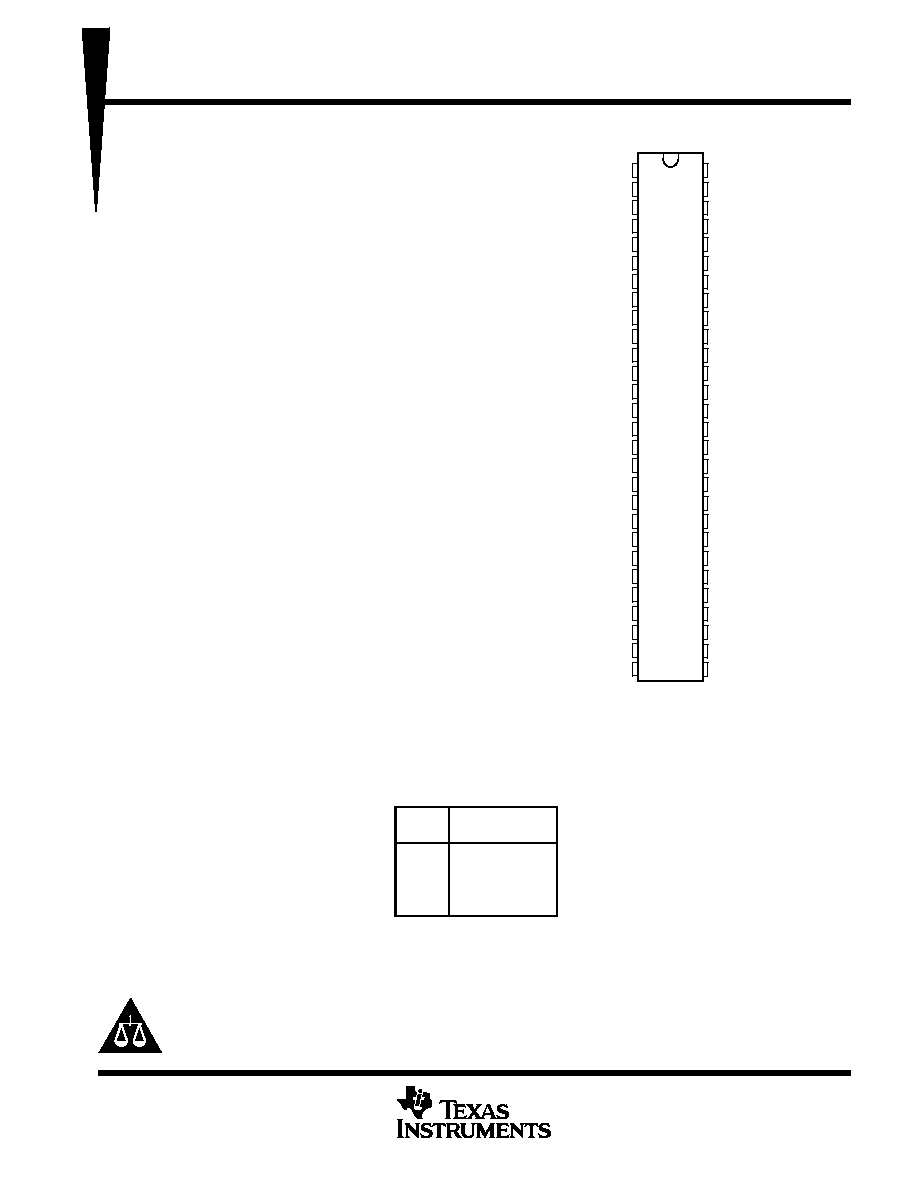
DGG, DGV, OR DL PACKAGE
(TOP VIEW)
1
2
3
4
5
6
7
8
9
10
11
12
13
14
15
16
17
18
19
20
21
22
23
24
25
26
27
28
56
55
54
53
52
51
50
49
48
47
46
45
44
43
42
41
40
39
38
37
36
35
34
33
32
31
30
29
S
1A
NC
2A
NC
3A
NC
GND
4A
NC
5A
NC
6A
NC
7A
NC
V
CC
8A
GND
NC
9A
NC
10A
NC
11A
NC
12A
NC
NC
NC
1B1
1B2
2B1
2B2
3B1
GND
3B2
4B1
4B2
5B1
5B2
6B1
6B2
7B1
7B2
8B1
GND
8B2
9B1
9B2
10B1
10B2
11B1
11B2
12B1
12B2
NC ≠ No internal connection

SN74CBTLVR16292
LOW-VOLTAGE 12-BIT 1-OF-2 FET MULTIPLEXER/DEMULTIPLEXER
WITH INTERNAL PULLDOWN RESISTORS
SCDS056D ≠ MARCH 1998 ≠ REVISED DECEMBER 1999
2
POST OFFICE BOX 655303
∑
DALLAS, TEXAS 75265
logic diagram (positive logic)
1A
SW
1B1
SW
1B2
SW
12B1
SW
12B2
12A
S
2
27
1
54
53
30
29
RINT
RINT
RINT
RINT
simplified schematic, each FET switch
A
(OE)
B

SN74CBTLVR16292
LOW-VOLTAGE 12-BIT 1-OF-2 FET MULTIPLEXER/DEMULTIPLEXER
WITH INTERNAL PULLDOWN RESISTORS
SCDS056D ≠ MARCH 1998 ≠ REVISED DECEMBER 1999
3
POST OFFICE BOX 655303
∑
DALLAS, TEXAS 75265
absolute maximum ratings over operating free-air temperature range (unless otherwise noted)
Supply voltage range, V
CC
≠0.5 V to 4.6 V
. . . . . . . . . . . . . . . . . . . . . . . . . . . . . . . . . . . . . . . . . . . . . . . . . . . . . . . . .
Input voltage range, V
I
(see Note 1)
≠0.5 V to 4.6 V
. . . . . . . . . . . . . . . . . . . . . . . . . . . . . . . . . . . . . . . . . . . . . . . . .
Continuous channel current
128 mA
. . . . . . . . . . . . . . . . . . . . . . . . . . . . . . . . . . . . . . . . . . . . . . . . . . . . . . . . . . . . . .
Input clamp current, I
IK
(V
I
< 0)
≠50 mA
. . . . . . . . . . . . . . . . . . . . . . . . . . . . . . . . . . . . . . . . . . . . . . . . . . . . . . . . . . .
Package thermal impedance,
JA
(see Note 2): DGG package
64
∞
C/W
. . . . . . . . . . . . . . . . . . . . . . . . . . . . . . .
DGV package
48
∞
C/W
. . . . . . . . . . . . . . . . . . . . . . . . . . . . . . . .
DL package
56
∞
C/W
. . . . . . . . . . . . . . . . . . . . . . . . . . . . . . . . .
Storage temperature range, T
stg
≠65
∞
C to 150
∞
C
. . . . . . . . . . . . . . . . . . . . . . . . . . . . . . . . . . . . . . . . . . . . . . . . . . .
Stresses beyond those listed under "absolute maximum ratings" may cause permanent damage to the device. These are stress ratings only, and
functional operation of the device at these or any other conditions beyond those indicated under "recommended operating conditions" is not
implied. Exposure to absolute-maximum-rated conditions for extended periods may affect device reliability.
NOTES:
1. The input and output negative-voltage ratings may be exceeded if the input and output clamp-current ratings are observed.
2. The package thermal impedance is calculated in accordance with JESD 51.
recommended operating conditions (see Note 3)
MIN
MAX
UNIT
VCC
Supply voltage
2.3
3.6
V
VIH
High level control input voltage
VCC = 2.3 V to 2.7 V
1.7
V
VIH
High-level control input voltage
VCC = 2.7 V to 3.6 V
2
V
VIL
Low level control input voltage
VCC = 2.3 V to 2.7 V
0.7
V
VIL
Low-level control input voltage
VCC = 2.7 V to 3.6 V
0.8
V
TA
Operating free-air temperature
≠40
85
∞
C
NOTE 3: All unused control inputs of the device must be held at VCC or GND to ensure proper device operation. Refer to the TI application report,
Implications of Slow or Floating CMOS Inputs, literature number SCBA004.
electrical characteristics over recommended operating free-air temperature range (unless
otherwise noted)
PARAMETER
TEST CONDITIONS
MIN
TYP
MAX
UNIT
VIK
VCC = 3 V,
II = ≠18 mA
≠1.2
V
II
VCC = 3.6 V,
VI = VCC or GND
±
1
µ
A
Ioff
VCC = 0,
VI or VO = 0 to 3.6 V
10
µ
A
ICC
VCC = 3.6 V,
IO = 0,
VI = VCC or GND
10
µ
A
ICCß
Control input
VCC = 3.6 V,
One input at 3 V,
Other inputs at VCC or GND
300
µ
A
Ci
Control input
VI = 3.3 V or 0
3.5
pF
Cio
A or B port
VO = 3.3 V or 0
23
pF
∂
V
2 3 V
VI = 0
II = 64 mA
30
47
∂
VCC = 2.3 V,
TYP at VCC = 2.5 V
VI = 0
II = 24 mA
30
47
r
∂
TYP at VCC = 2.5 V
VI = 1.7 V,
II = 15 mA
36
80
ron∂
VI = 0
II = 64 mA
30
42
VCC = 3 V
VI = 0
II = 24 mA
30
42
VI = 2.4 V,
II = 15 mA
32
47
All typical values are at VCC = 3.3 V (unless otherwise noted), TA = 25
∞
C.
ß This is the increase in supply current for each input that is at the specified voltage level rather than VCC or GND.
∂ Measured by the voltage drop between the A and B terminals at the indicated current through the switch. On-state resistance is determined by
the lower of the voltages of the two (A or B) terminals.

SN74CBTLVR16292
LOW-VOLTAGE 12-BIT 1-OF-2 FET MULTIPLEXER/DEMULTIPLEXER
WITH INTERNAL PULLDOWN RESISTORS
SCDS056D ≠ MARCH 1998 ≠ REVISED DECEMBER 1999
4
POST OFFICE BOX 655303
∑
DALLAS, TEXAS 75265
switching characteristics over recommended operating free-air temperature range (unless
otherwise noted) (see Figures 1 and 2)
PARAMETER
FROM
(INPUT)
TO
(OUTPUT)
VCC = 2.5 V
±
0.2 V
VCC = 3.3 V
±
0.3 V
UNIT
(INPUT)
(OUTPUT)
MIN
MAX
MIN
MAX
tpd
A or B
B or A
0.9
1.5
ns
tpd
S
A
3.2
8.5
3.2
8
ns
ten
S
B
1
6.5
1
5.8
ns
tdis
S
B
1
5.3
1
4.6
ns
The propagation delay is the calculated RC time constant of the typical on-state resistance of the switch and the specified load capacitance, when
driven by an ideal voltage source (zero output impedance).
This propagation delay was measured by observing the change of voltage on the A output introduced by static levels equal to 3 V or 0 for
3.3 V
±
0.3 V or VCC, or 0 for 2.5 V
±
0.2 V on B1 and B2 to achieve the desired transition.
switching characteristics over recommended operating free-air temperature range (unless
otherwise noted) (see Figures 1 and 2)
PARAMETER
DESCRIPTION
VCC = 2.5 V
±
0.2 V
VCC = 3.3 V
±
0.3 V
UNIT
MIN
MAX
MIN
MAX
tmbbß
Make-before-break time
0
2
0
2
ns
ß The make-before-break time is the time interval between make and break during the transition from one selected port to the other.

SN74CBTLVR16292
LOW-VOLTAGE 12-BIT 1-OF-2 FET MULTIPLEXER/DEMULTIPLEXER
WITH INTERNAL PULLDOWN RESISTORS
SCDS056D ≠ MARCH 1998 ≠ REVISED DECEMBER 1999
5
POST OFFICE BOX 655303
∑
DALLAS, TEXAS 75265
PARAMETER MEASUREMENT INFORMATION
V
CC
= 2.5 V
±
0.2 V
VCC/3
VCC/3
VCC/2
VCC/2
VOH
VOL
From Output
Under Test
CL = 30 pF
(see Note A)
LOAD CIRCUIT
S1
Open
GND
500
500
Output
Control
Output
Waveform 1
S1 at 2
◊
VCC
(see Note B)
Output
Waveform 2
S1 at GND
(see Note B)
tPZL
tPZH
tPLZ
tPHZ
0 V
VOL + 0.15 V
VOH ≠ 0.15 V
0 V
VCC
VOLTAGE WAVEFORMS
ENABLE AND DISABLE TIMES
tpd
tPLZ/tPZL
tPHZ/tPZH
Open
2
◊
VCC
GND
TEST
S1
NOTES: A. CL includes probe and jig capacitance.
B. Waveform 1 is for an output with internal conditions such that the output is low except when disabled by the output control.
Waveform 2 is for an output with internal conditions such that the output is high except when disabled by the output control.
C. All input pulses are supplied by generators having the following characteristics: PRR
10 MHz, ZO = 50
, tr
2 ns, tf
2 ns.
D. The outputs are measured one at a time with one transition per measurement.
E. tPLZ and tPHZ are the same as tdis.
F. tPZL and tPZH are the same as ten.
G. tPLH and tPHL are the same as tpd.
tPHL
VCC/2
VCC/2
VCC
0 V
VOH
VOL
Input
Output
VOLTAGE WAVEFORMS
PROPAGATION DELAY TIMES
VCC/2
VCC/2
tPLH
2
◊
VCC
2
◊
VCC/3
Figure 1. Load Circuit and Voltage Waveforms