
SN74HC4066
QUADRUPLE BILATERAL ANALOG SWITCH
SCLS325G ≠ MARCH 1996 ≠ REVISED JULY 2003
1
POST OFFICE BOX 655303
∑
DALLAS, TEXAS 75265
D
Wide Operating Voltage Range of 2 V to 6 V
D
Typical Switch Enable Time of 18 ns
D
Low Power Consumption, 20-
µ
A Max I
CC
D
Low Input Current of 1
µ
A Max
D
High Degree of Linearity
D
High On-Off Output-Voltage Ratio
D
Low Crosstalk Between Switches
D
Low On-State Impedance . . .
50-
TYP at V
CC
= 6 V
D
Individual Switch Controls
description/ordering information
The SN74HC4066 is a silicon-gate CMOS quadruple analog switch designed to handle both analog and digital
signals. Each switch permits signals with amplitudes of up to 6 V (peak) to be transmitted in either direction.
Each switch section has its own enable input control (C). A high-level voltage applied to C turns on the
associated switch section.
Applications include signal gating, chopping, modulation or demodulation (modem), and signal multiplexing for
analog-to-digital and digital-to-analog conversion systems.
ORDERING INFORMATION
TA
PACKAGE
ORDERABLE
PART NUMBER
TOP-SIDE
MARKING
PDIP ≠ N
Tube of 25
SN74HC4066N
SN74HC4066N
Tube of 50
SN74HC4066D
SOIC ≠ D
Reel of 2500
SN74HC4066DR
HC4066
Reel of 250
SN74HC4066DT
≠40
∞
C to 85
∞
C
SOP ≠ NS
Reel of 2000
SN74HC4066NSR
HC4066
SSOP ≠ DB
Reel of 2000
SN74HC4066DBR
HC4066
Tube of 90
SN74HC4066PW
TSSOP ≠ PW
Reel of 2000
SN74HC4066PWR
HC4066
Reel of 250
SN74HC4066PWT
Package drawings, standard packing quantities, thermal data, symbolization, and PCB design
guidelines are available at www.ti.com/sc/package.
FUNCTION TABLE
(each switch)
INPUT
CONTROL
(C)
SWITCH
L
OFF
H
ON
Copyright
2003, Texas Instruments Incorporated
PRODUCTION DATA information is current as of publication date.
Products conform to specifications per the terms of Texas Instruments
standard warranty. Production processing does not necessarily include
testing of all parameters.
Please be aware that an important notice concerning availability, standard warranty, and use in critical applications of
Texas Instruments semiconductor products and disclaimers thereto appears at the end of this data sheet.
1
2
3
4
5
6
7
14
13
12
11
10
9
8
1A
1B
2B
2A
2C
3C
GND
V
CC
1C
4C
4A
4B
3B
3A
D, DB, N, NS, OR PW PACKAGE
(TOP VIEW)

SN74HC4066
QUADRUPLE BILATERAL ANALOG SWITCH
SCLS325G ≠ MARCH 1996 ≠ REVISED JULY 2003
2
POST OFFICE BOX 655303
∑
DALLAS, TEXAS 75265
logic diagram, each switch (positive logic)
A
VCC
VCC
B
One of Four Switches
C
absolute maximum ratings over operating free-air temperature range (unless otherwise noted)
Supply voltage range, V
CC
(see Note 1)
≠0.5 V to 7 V
. . . . . . . . . . . . . . . . . . . . . . . . . . . . . . . . . . . . . . . . . . . . . .
Control-input diode current, I
I
(V
I
< 0 or V
I
> V
CC
)
±
20 mA
. . . . . . . . . . . . . . . . . . . . . . . . . . . . . . . . . . . . . . . . . . .
I/O port diode current, I
I
(V
I
< 0 or V
I/O
> V
CC
)
±
20 mA
. . . . . . . . . . . . . . . . . . . . . . . . . . . . . . . . . . . . . . . . . . . . . .
On-state switch current (V
I/O
= 0 to V
CC
)
±
25 mA
. . . . . . . . . . . . . . . . . . . . . . . . . . . . . . . . . . . . . . . . . . . . . . . . . .
Continuous current through V
CC
or GND
±
50 mA
. . . . . . . . . . . . . . . . . . . . . . . . . . . . . . . . . . . . . . . . . . . . . . . . . . .
Package thermal impedance,
JA
(see Note 2): D package
86
∞
C/W
. . . . . . . . . . . . . . . . . . . . . . . . . . . . . . . . . . .
DB package
96
∞
C/W
. . . . . . . . . . . . . . . . . . . . . . . . . . . . . . . . .
N package
80
∞
C/W
. . . . . . . . . . . . . . . . . . . . . . . . . . . . . . . . . . .
NS package
76
∞
C/W
. . . . . . . . . . . . . . . . . . . . . . . . . . . . . . . . .
PW package
113
∞
C/W
. . . . . . . . . . . . . . . . . . . . . . . . . . . . . . . .
Storage temperature range, T
stg
≠65
∞
C to 150
∞
C
. . . . . . . . . . . . . . . . . . . . . . . . . . . . . . . . . . . . . . . . . . . . . . . . . . .
Stresses beyond those listed under "absolute maximum ratings" may cause permanent damage to the device. These are stress ratings only, and
functional operation of the device at these or any other conditions beyond those indicated under "recommended operating conditions" is not
implied. Exposure to absolute-maximum-rated conditions for extended periods may affect device reliability.
NOTES:
1. All voltages are with respect to ground unless otherwise specified.
2. The package thermal impedance is calculated in accordance with JESD 51-7.

SN74HC4066
QUADRUPLE BILATERAL ANALOG SWITCH
SCLS325G ≠ MARCH 1996 ≠ REVISED JULY 2003
3
POST OFFICE BOX 655303
∑
DALLAS, TEXAS 75265
recommended operating conditions (see Note 3)
MIN
NOM
MAX
UNIT
VCC
Supply voltage
2
5
6
V
VI/O
I/O port voltage
0
VCC
V
VCC = 2 V
1.5
VCC
VIH
High-level input voltage, control inputs
VCC = 4.5 V
3.15
VCC
V
VCC = 6 V
4.2
VCC
VCC = 2 V
0
0.3
VIL
Low-level input voltage, control inputs
VCC = 4.5 V
0
0.9
V
VCC = 6 V
0
1.2
VCC = 2 V
1000
t/
v
Input transition rise/fall time
VCC = 4.5 V
500
ns
VCC = 6 V
400
TA
Operating free-air temperature
≠40
85
∞
C
With supply voltages at or near 2 V, the analog switch on-state resistance becomes very nonlinear. It is recommended that only digital signals
be transmitted at these low supply voltages.
NOTE 3: All unused inputs of the device must be held at VCC or GND to ensure proper device operation. Refer to the TI application report,
Implications of Slow or Floating CMOS Inputs, literature number SCBA004.
electrical characteristics over recommended operating free-air temperature range (unless
otherwise noted)
PARAMETER
TEST CONDITIONS
V
TA = 25
_
C
MIN
MAX
UNIT
PARAMETER
TEST CONDITIONS
VCC
MIN
TYP
MAX
MIN
MAX
UNIT
I
1
A V
0 t V
2 V
150
ron
On-state switch resistance
IT = ≠1 mA, VI = 0 to VCC,
VC = VIH (see Figure 1)
4.5 V
50
85
106
VC = VIH (see Figure 1)
6 V
30
V
V
GND V
V
2 V
320
ron(p)
Peak on-state resistance
VI = VCC or GND, VC = VIH,
IT = ≠1 mA
4.5 V
70
170
215
( )
IT = ≠1 mA
6 V
50
II
Control input current
VC = 0 or VCC
6 V
±
0.1
±
100
±
1000
nA
Isoff
Off-state switch leakage current
VI = VCC or 0, VO = VCC or 0,
VC = VIL (see Figure 2)
6 V
±
0.1
±
5
µ
A
Ison
On-state switch leakage current
VI = VCC or 0, VC = VIH
(see Figure 3)
6 V
±
0.1
±
5
µ
A
ICC
Supply current
VI = 0 or VCC,
IO = 0
6 V
2
20
µ
A
Ci
Input capacitance
A or B
5 V
9
pF
Ci
Input capacitance
C
5 V
3
10
10
pF
Cf
Feed-through
capacitance
A to B
VI = 0
0.5
pF
Co
Output capacitance
A or B
5 V
9
pF

SN74HC4066
QUADRUPLE BILATERAL ANALOG SWITCH
SCLS325G ≠ MARCH 1996 ≠ REVISED JULY 2003
4
POST OFFICE BOX 655303
∑
DALLAS, TEXAS 75265
switching characteristics over recommended operating free-air temperature range
PARAMETER
FROM
TO
TEST
VCC
TA = 25
_
C
MIN
MAX
UNIT
PARAMETER
(INPUT)
(OUTPUT)
CONDITIONS
VCC
MIN
TYP
MAX
MIN
MAX
UNIT
t
P
ti
C
50 F
2 V
10
60
75
tPLH,
tPHL
Propagation
delay time
A or B
B or A
CL = 50 pF
(see Figure 4)
4.5 V
4
12
15
ns
tPHL
delay time
(see Figure 4)
6 V
3
10
13
t
S it h
RL = 1 k
,
2 V
70
180
225
tPZH,
tPZL
Switch
turn-on time
C
A or B
RL = 1 k
,
CL = 50 pF
4.5 V
21
36
45
ns
tPZL
turn-on time
L
(see Figure 5)
6 V
18
31
38
t
S it h
RL = 1 k
,
2 V
50
200
250
tPLZ,
tPHZ
Switch
turn-off time
C
A or B
RL = 1 k
,
CL = 50 pF
4.5 V
25
40
50
ns
tPHZ
turn-off time
L
(see Figure 5)
6 V
22
34
43
Control
CL = 15 pF,
RL = 1 k
2 V
15
fI
Control
input
frequency
C
A or B
RL = 1 k
,
VC = VCC or GND,
V
V
/2
4.5 V
30
MHz
frequency
VO = VCC/2
(see Figure 6)
6 V
30
Control
feed-through
C
A or B
CL = 50 pF,
Rin = RL = 600
,
VC = VCC or GND
4.5 V
15
mV
feed-through
noise
C
A or B
VC = VCC or GND,
fin = 1 MHz
(see Figure 7)
6 V
20
(rms)
operating characteristics, V
CC
= 4.5 V, T
A
= 25
∞
C
PARAMETER
TEST CONDITIONS
TYP
UNIT
Cpd
Power dissipation capacitance per gate
CL = 50 pF,
f = 1 MHz
45
pF
Minimum through bandwidth, A to B or B to A [20 log (VO/VI)] = ≠3 dB
CL = 50 pF,
VC = VCC
RL = 600
,
(see Figure 8)
30
MHz
Crosstalk between any switches
CL = 10 pF,
fin = 1 MHz
RL = 50
,
(see Figure 9)
45
dB
Feed through, switch off, A to B or B to A
CL = 50 pF,
fin = 1 MHz
RL = 600
,
(see Figure 10)
42
dB
Amplitude distortion rate, A to B or B to A
CL = 50 pF,
fin = 1 kHz
RL = 10 k
,
(see Figure 11)
0.05%
Adjust the input amplitude for output = 0 dBm at f = 1 MHz. Input signal must be a sine wave.
Adjust the input amplitude for input = 0 dBm at f = 1 MHz. Input signal must be a sine wave.
SN74HC4066
QUADRUPLE BILATERAL ANALOG SWITCH
SCLS325G ≠ MARCH 1996 ≠ REVISED JULY 2003
5
POST OFFICE BOX 655303
∑
DALLAS, TEXAS 75265
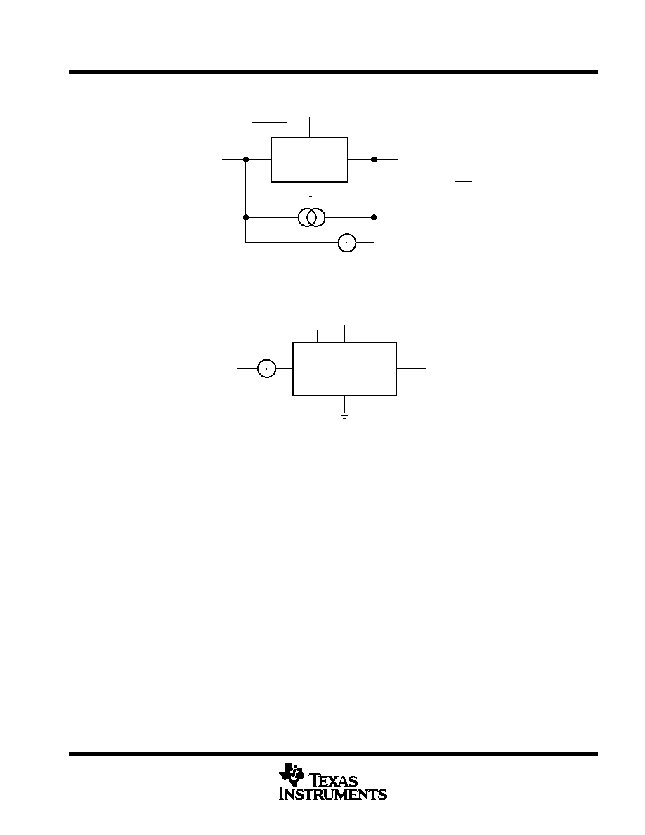
PARAMETER MEASUREMENT INFORMATION
VCC
VI = VCC
VC = VIH
1.0 mA
≠
+
VO
r
on
+
V
I≠O
10
≠3
W
VI≠O
VCC
GND
(ON)
V
Figure 1. On-State Resistance Test Circuit
VCC
VC = VIL
A
B
VS = VA ≠ VB
CONDITION 1: VA = 0, VB = VCC
CONDITION 2: VA = VCC, VB = 0
VCC
GND
(OFF)
A
Figure 2. Off-State Switch Leakage-Current Test Circuit