SN54HCT273, SN74HCT273
OCTAL D-TYPE FLIP-FLOPS
WITH CLEAR
SCLS068C ≠ NOVEMBER 1988 ≠ REVISED MAY 1997
1
POST OFFICE BOX 655303
∑
DALLAS, TEXAS 75265
D
Inputs Are TTL-Voltage Compatible
D
Contain Eight D-Type Flip-Flops
D
Direct Clear Input
D
Applications Include:
≠ Buffer/Storage Registers
≠ Shift Registers
≠ Pattern Generators
D
Package Options Include Plastic
Small-Outline (DW) and Ceramic Flat (W)
Packages, Ceramic Chip Carriers (FK), and
Standard Plastic (N) and Ceramic (J)
300-mil DIPs
description
These devices are positive-edge-triggered D-type
flip-flops with a common enable input. The
'HCT273 are similar to the 'HCT377, but feature
a common clear enable (CLR) input instead of a
latched clock.
Information at the data (D) inputs meeting the
setup time requirements is transferred to the
Q outputs on the positive-going edge of the clock
(CLK) pulse. Clock triggering occurs at a
particular voltage level and is not directly related
to the positive-going pulse. When CLK is at either
the high or low level, the D input has no effect at
the output. The circuits are designed to prevent
false clocking by transitions at CLR.
The SN54HCT273 is characterized for operation over the full military temperature range of ≠55
∞
C to 125
∞
C. The
SN74HCT273 is characterized for operation from ≠40
∞
C to 85
∞
C.
FUNCTION TABLE
(each flip-flop)
INPUTS
OUTPUT
CLR
CLK
D
Q
L
X
X
L
H
H
H
H
L
L
H
L
X
Q0
1
2
3
4
5
6
7
8
9
10
20
19
18
17
16
15
14
13
12
11
CLR
1Q
1D
2D
2Q
3Q
3D
4D
4Q
GND
V
CC
8Q
8D
7D
7Q
6Q
6D
5D
5Q
CLK
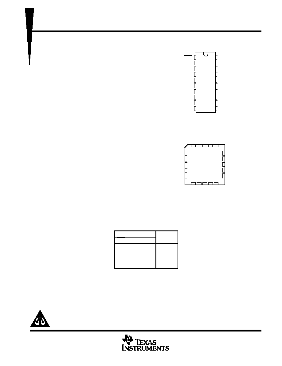
SN54HCT273 . . . J OR W PACKAGE
SN74HCT273 . . . DW, N, OR PW PACKAGE
(TOP VIEW)
3
2 1 20 19
9 10 11 12 13
4
5
6
7
8
18
17
16
15
14
8D
7D
7Q
6Q
6D
2D
2Q
3Q
3D
4D
1D
1Q
CLR
5Q
5D
8Q
4Q
GND
CLK
V
CC
SN54HCT273 . . . FK PACKAGE
(TOP VIEW)
Copyright
©
1997, Texas Instruments Incorporated
Please be aware that an important notice concerning availability, standard warranty, and use in critical applications of
Texas Instruments semiconductor products and disclaimers thereto appears at the end of this data sheet.
UNLESS OTHERWISE NOTED this document contains PRODUCTION
DATA information current as of publication date. Products conform to
specifications per the terms of Texas Instruments standard warranty.
Production processing does not necessarily include testing of all
parameters.

SN54HCT273, SN74HCT273
OCTAL D-TYPE FLIP-FLOPS
WITH CLEAR
SCLS068C ≠ NOVEMBER 1988 ≠ REVISED MAY 1997
2
POST OFFICE BOX 655303
∑
DALLAS, TEXAS 75265
logic symbol
1D
3
1D
11
CLK
C1
R
1
1Q
2
4
2D
2Q
5
7
3D
3Q
6
8
4D
4Q
9
13
5D
5Q
12
14
6D
6Q
15
17
7D
7Q
16
18
8D
8Q
19
CLR
This symbol is in accordance with ANSI/IEEE Std 91-1984 and IEC Publication 617-12.
logic diagram (positive logic)
CLK
1D
3
1D
C1
R
1Q
2
2D
4
1D
C1
R
2Q
5
3D
7
1D
C1
R
3Q
6
4D
8
1D
C1
R
4Q
9
5D
13
1D
C1
R
5Q
12
6D
14
1D
C1
R
6Q
15
7D
17
1D
C1
R
7Q
16
8D
18
1D
C1
R
8Q
19
CLR
11
1
logic diagram, each flip-flop (positive logic)
CLK(I)
R
Q
C
C
D
C
C
C
C
C
C
TG
TG
TG
TG
C
C

SN54HCT273, SN74HCT273
OCTAL D-TYPE FLIP-FLOPS
WITH CLEAR
SCLS068C ≠ NOVEMBER 1988 ≠ REVISED MAY 1997
3
POST OFFICE BOX 655303
∑
DALLAS, TEXAS 75265
absolute maximum ratings over operating free-air temperature range
Supply voltage range, V
CC
≠0.5 V to 7 V
. . . . . . . . . . . . . . . . . . . . . . . . . . . . . . . . . . . . . . . . . . . . . . . . . . . . . . . . . .
Input clamp current, I
IK
(V
I
< 0 or V
I
> V
CC
) (see Note 1)
±
20 mA
. . . . . . . . . . . . . . . . . . . . . . . . . . . . . . . . . . . .
Output clamp current, I
OK
(V
O
< 0 or V
O
> V
CC
) (see Note 1)
±
20 mA
. . . . . . . . . . . . . . . . . . . . . . . . . . . . . . . .
Continuous output current, I
O
(V
O
= 0 to V
CC
)
±
25 mA
. . . . . . . . . . . . . . . . . . . . . . . . . . . . . . . . . . . . . . . . . . . . . .
Continuous current through V
CC
or GND
±
50 mA
. . . . . . . . . . . . . . . . . . . . . . . . . . . . . . . . . . . . . . . . . . . . . . . . . . .
Package thermal impedance,
JA
(see Note 2): DW package
97
∞
C/W
. . . . . . . . . . . . . . . . . . . . . . . . . . . . . . . . .
N package
67
∞
C/W
. . . . . . . . . . . . . . . . . . . . . . . . . . . . . . . . . . .
PW package
128
∞
C/W
. . . . . . . . . . . . . . . . . . . . . . . . . . . . . . . .
Storage temperature range, T
stg
≠65
∞
C to 150
∞
C
. . . . . . . . . . . . . . . . . . . . . . . . . . . . . . . . . . . . . . . . . . . . . . . . . . .
Stresses beyond those listed under "absolute maximum ratings" may cause permanent damage to the device. These are stress ratings only, and
functional operation of the device at these or any other conditions beyond those indicated under "recommended operating conditions" is not
implied. Exposure to absolute-maximum-rated conditions for extended periods may affect device reliability.
NOTES:
1. The input and output voltage ratings may be exceeded if the input and output current ratings are observed.
2. The package thermal impedance is calculated in accordance with JESD 51, except for through-hole packages, which use a trace
length of zero.
recommended operating conditions
SN54HCT273
SN74HCT273
UNIT
MIN
NOM
MAX
MIN
NOM
MAX
UNIT
VCC
Supply voltage
4.5
5
5.5
4.5
5
5.5
V
VIH
High-level input voltage
VCC = 4.5 V to 5.5 V
2
2
V
VIL
Low-level input voltage
VCC = 4.5 V to 5.5 V
0
0.8
0
0.8
V
VI
Input voltage
0
VCC
0
VCC
V
VO
Output voltage
0
VCC
0
VCC
V
tt
Input transition (rise and fall) times
0
500
0
500
ns
TA
Operating free-air temperature
≠55
125
≠40
85
∞
C
electrical characteristics over recommended operating free-air temperature range (unless
otherwise noted)
PARAMETER
TEST CONDITIONS
VCC
TA = 25
∞
C
SN54HCT273
SN74HCT273
UNIT
PARAMETER
TEST CONDITIONS
VCC
MIN
TYP
MAX
MIN
MAX
MIN
MAX
UNIT
VOH
VI = VIH or VIL
IOH = ≠20
µ
A
4.5 V
4.4
4.499
4.4
4.4
V
VOH
VI = VIH or VIL
IOH = ≠4 mA
4.5 V
3.98
4.30
3.7
3.84
V
VOL
VI = VIH or VIL
IOL = 20
µ
A
4.5 V
0.001
0.1
0.1
0.1
V
VOL
VI = VIH or VIL
IOL = 4 mA
4.5 V
0.17
0.26
0.4
0.33
V
II
VI = VCC or 0
5.5 V
±
0.1
±
100
±
1000
±
1000
nA
ICC
VI = VCC or 0,
IO = 0
5.5 V
8
160
80
µ
A
ICC
One input at 0.5 V or 2.4 V,
Other inputs at 0 or VCC
5.5 V
1.4
2.4
3
2.9
mA
Ci
4.5 V
to 5.5 V
3
10
10
10
pF
This is the increase in supply current for each input that is at one of the specified TTL voltage levels rather than 0 V or VCC.
PRODUCT PREVIEW information concerns products in the formative or
design phase of development. Characteristic data and other
specifications are design goals. Texas Instruments reserves the right to
change or discontinue these products without notice.

SN54HCT273, SN74HCT273
OCTAL D-TYPE FLIP-FLOPS
WITH CLEAR
SCLS068C ≠ NOVEMBER 1988 ≠ REVISED MAY 1997
4
POST OFFICE BOX 655303
∑
DALLAS, TEXAS 75265
timing requirements over recommended operating free-air temperature range (unless otherwise
noted)
VCC
TA = 25
∞
C
SN54HCT273
SN74HCT273
UNIT
VCC
MIN
MAX
MIN
MAX
MIN
MAX
UNIT
f l k
Clock frequency
4.5 V
0
25
0
16
0
20
MHz
fclock
Clock frequency
5.5 V
0
28
0
19
0
23
MHz
CLK high or low
4.5 V
20
30
25
t
Pulse duration
CLK high or low
5.5 V
18
25
22
ns
tw
Pulse duration
CLR low
4.5 V
16
24
20
ns
CLR low
5.5 V
14
20
17
Data
4.5 V
20
30
25
t
Setup time before CLK
Data
5.5 V
17
25
21
ns
tsu
Setup time before CLK
CLR inactive
4.5 V
20
30
25
ns
CLR inactive
5.5 V
17
25
21
th
Hold time data after CLK
4.5 V
0
0
0
ns
th
Hold time data after CLK
5.5 V
0
0
0
ns
switching characteristics over recommended operating free-air temperature range, V
CC
= 5 V
±
0.5 V,
C
L
= 50 pF (unless otherwise noted) (see Figure 1)
FROM
TO
SN54HCT273
PARAMETER
FROM
(INPUT)
TO
(OUTPUT)
VCC
TA = 25
∞
C
MIN
MAX
UNIT
(INPUT)
(OUTPUT)
MIN
TYP
MAX
MIN
MAX
f
4.5 V
25
31
16
MHz
fmax
5.5 V
28
37
19
MHz
t d
CLR
Any
4.5 V
15
34
50
ns
tpd
CLR
Any
5.5 V
12
29
42
ns
tPHL
CLR
Any
4.5 V
17
15
50
ns
tPHL
CLR
Any
5.5 V
15
34
42
ns
tt
Any
4.5 V
8
18
22
ns
tt
Any
5.5 V
7
19
21
ns
switching characteristics over recommended operating free-air temperature range, V
CC
= 5 V
±
0.5 V,
C
L
= 50 pF (unless otherwise noted) (see Figure 1)
FROM
TO
SN74HCT273
PARAMETER
FROM
(INPUT)
TO
(OUTPUT)
VCC
TA = 25
∞
C
MIN
MAX
UNIT
(INPUT)
(OUTPUT)
MIN
TYP
MAX
MIN
MAX
f
4.5 V
25
31
20
MHz
fmax
5.5 V
28
37
23
MHz
t d
CLR
Any
4.5 V
15
34
42
ns
tpd
CLR
Any
5.5 V
12
29
36
ns
tPHL
CLR
Any
4.5 V
17
34
42
ns
tPHL
CLR
Any
5.5 V
15
29
36
ns
tt
Any
4.5 V
8
15
19
ns
tt
Any
5.5 V
7
14
17
ns
PRODUCT PREVIEW information concerns products in the formative or
design phase of development. Characteristic data and other
specifications are design goals. Texas Instruments reserves the right to
change or discontinue these products without notice.
SN54HCT273, SN74HCT273
OCTAL D-TYPE FLIP-FLOPS
WITH CLEAR
SCLS068C ≠ NOVEMBER 1988 ≠ REVISED MAY 1997
5
POST OFFICE BOX 655303
∑
DALLAS, TEXAS 75265
operating characteristics, V
CC
= 5 V, T
A
= 25
∞
C
PARAMETER
TEST CONDITIONS
TYP
UNIT
Cpd
Power dissipation capacitance
No load
30
pF
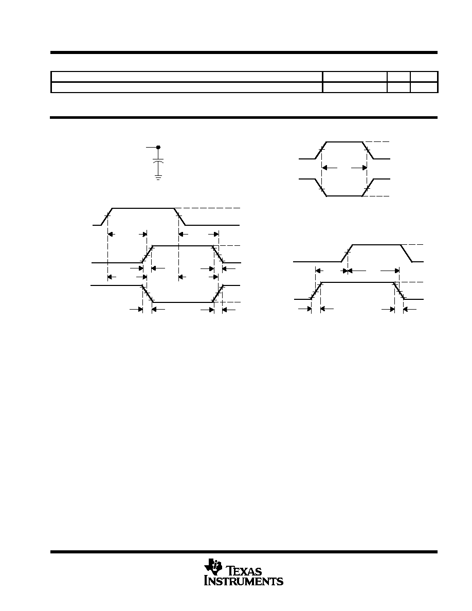
PARAMETER MEASUREMENT INFORMATION
VOLTAGE WAVEFORMS
SETUP AND HOLD AND INPUT RISE AND FALL TIMES
VOLTAGE WAVEFORMS
PULSE DURATIONS
th
tsu
1.3 V
1.3 V
1.3 V
0.3 V
0.3 V
2.7 V
2.7 V
3 V
3 V
0 V
0 V
tr
tf
Reference
Input
Data
Input
1.3 V
High-Level
Pulse
1.3 V
3 V
0 V
1.3 V
1.3 V
3 V
0 V
tw
Low-Level
Pulse
VOLTAGE WAVEFORMS
PROPAGATION DELAY AND OUTPUT RISE AND FALL TIMES
1.3 V
1.3 V
1.3 V
10%
10%
90%
90%
3 V
VOH
VOL
0 V
tr
tf
Input
In-Phase
Output
1.3 V
tPLH
tPHL
1.3 V
1.3 V
10%
10%
90%
90%
VOH
VOL
tr
tf
tPHL
tPLH
Out-of-
Phase
Output
Test
Point
From Output
Under Test
CL = 50 pF
(see Note A)
LOAD CIRCUIT
NOTES: A. CL includes probe and test-fixture capacitance.
B. Phase relationships between waveforms were chosen arbitrarily. All input pulses are supplied by generators having the following
characteristics: PRR
1 MHz, ZO = 50
, tr = 6 ns, tf = 6 ns.
C. The outputs are measured one at a time with one input transition per measurement.
D. For clock inputs, fmax is measured when the input duty cycle is 50%.
E. tPLH and tPHL are the same as tpd.
Figure 1. Load Circuit and Voltage Waveforms